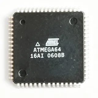
ATMEGA8515L-8AI - AVR 8-Bit MCU, 8KB Flash, 8MHz | Microchip
MPN: ATMEGA8515L-8AI ✓ 啟用中ATMEGA8515L-8AI 概覽
A microcontroller is a single-chip computer that integrates a processor core, memory, and programmable peripherals into one package, sitting at the heart of embedded systems in the broader hierarchy of semiconductors -> integrated circuits -> microcontrollers. The AVR architecture executes most of its 130 powerful instructions in a single clock cycle, so the ATmega8515L achieves up to 8 MIPS throughput at 8 MHz - roughly 1 MIPS per MHz - making it far more efficient per clock than many CISC 8-bit designs.
Key features include self-programming Flash for field firmware updates, a full-duplex USART, SPI serial interface, one 16-bit and two 8-bit timers with PWM capability, an 8-channel 10-bit ADC replacement via external memory-mapped peripherals, and 35 programmable I/O lines. The external memory bus with address latching control distinguishes this family from smaller ATmega parts such as the ATmega8.
Architecturally, the ATmega8515 is a low-power CMOS device based on the AVR enhanced RISC core with 32 general-purpose working registers directly connected to the ALU, fully static operation down to DC, and a Harvard bus structure separating program and data paths.
Typical applications include industrial control panels, legacy AVR system maintenance and re-manufacturing, motor control interfaces, and external-memory expansion designs where the 64 KB SRAM bus is essential.
For design, note the 'L' suffix limits clocking to 8 MHz - never substitute a 16 MHz grade part in a timing-critical firmware build without recalculating UART baud rates and timer constants.
This page adds distributor stock data, pin-compatible ATmega8515 family drop-in alternatives, comparison tables, and practical design notes not found in the manufacturer datasheet.
直接替換替代品,適用於 ATMEGA8515L-8AI — 相同封裝,腳位對腳位相容。需重新設計 PCB 的不同封裝零件不列入。
此系列的變體
與下列產品可直接替換的同系列型號: ATMEGA8515L-8AI (相同外形與佔位) — 差異在於 Package, Throughput, Instructions, Operating Temperature, General Purpose I/O.
ATMEGA8515L-8AU
✅ 直接替換📋 參考替代品(不在目錄中)
ATMEGA8515-16AUR
✅ 直接替換聯絡詢價
查看資料表 →ATMEGA8515-16JI
✅ 直接替換聯絡詢價
查看資料表 →ATMEGA8515-16AI
✅ 直接替換 ⚠️ 規格未經驗證聯絡詢價
查看資料表 →AT90S8515-8AI
✅ 直接替換📋 參考替代品(不在目錄中)
ATMEGA8515L-8AI 最大額定值與電氣特性
| Core Architecture | 8-bit AVR RISC |
| Program Memory (Flash) | 8 KB (4K x 16) In-System Programmable |
| SRAM | 544 bytes internal |
| External SRAM Support | up to 64 KB |
| EEPROM | 512 bytes |
| 最大時脈頻率 | 8 MHz |
| Throughput | up to 8 MIPS at 8 MHz (16 MIPS at 16 MHz for 16 MHz grades) |
| Operating Voltage Range | 2.7 V to 5.5 V |
| 工作溫度 | -40C to +85C (industrial) |
| Instructions | 130 powerful instructions, most single-cycle |
| General Purpose I/O | 35 programmable I/O lines |
| Timers/Counters | 2 x 8-bit, 1 x 16-bit with PWM |
| Serial Interfaces | USART, SPI |
| 封裝 | 44-TQFP (10 x 10 mm) |
| 安裝類型 | Surface Mount |
| RoHS 狀態 | RoHS compliant (lead-free 'I' suffix per Microchip nomenclature) |
| In-Circuit Programming | ICSP via SPI (supported by MPLAB SNAP / AVR programmers) |
ATMEGA8515L-8AI 44-tqfp (10 x 10 mm) 腳位配置指南
ATMEGA8515L-8AI(44-tqfp (10 x 10 mm) 封裝)的腳位配置。 此數位 IC 包含 GPIO、通訊介面(UART、SPI、I2C)與電源腳位。替代腳位功能與配置選項請參閱製造商資料表。對嵌入式系統設計與 PCB 佈局至關重要。

無詳細腳位定義資料: ATMEGA8515L-8AI.
請參閱 資料表 以查看完整腳位配置。
典型應用
ATMEGA8515L-8AI 適用於 6 應用s: Industrial Control Panels, Legacy AVR System Maintenance, External Memory Expansion Designs, Serial Communication Gateways, Timer and PWM-Based Motion Interfaces, Embedded Instrumentation and Test Fixtures.
Industrial Control Panels
The ATMEGA8515L-8AI fits industrial control panel designs where a 5 V or 3.3 V logic environment, wide -40C to +85C temperature rating, and 35 programmable I/O lines drive relays, contactors, and status indicators. Its 2.7 V to 5.5 V supply tolerance absorbs industrial rail sag, while the USART links to HMI displays and the SPI bus to ADCs or EEPROM. The 64 KB external memory interface supports event log buffers in external SRAM, and the 512 B EEPROM retains calibration and configuration data through power cycles without external non-volatile components.
推薦
Legacy AVR System Maintenance
Many installed AVR-based products from the 2000s were built around the ATmega8515, and the ATMEGA8515L-8AI is the correct re-stocking part for repair and re-manufacturing lines. It preserves the exact 44-TQFP footprint, register map, and 8 MHz L-grade timing, so existing firmware binaries program without recompilation. The In-System Programmable Flash allows field firmware updates via the SPI ICSP interface using tools such as MPLAB SNAP. Compared with switching to a modern ATmega, this part eliminates PCB respins and requalification for service-stock and obsolescence-management programs.
推薦
External Memory Expansion Designs
The external memory bus is the ATmega8515's signature capability: ports A and C form a multiplexed data/address bus with ALE, RD, and WR strobes, addressing up to 64 KB of external SRAM. The ATMEGA8515L-8AI suits data-acquisition buffers, protocol analyzers, and dataloggers needing far more than its 544 bytes of internal SRAM. Designers latch the low address byte with a 74HC573-class latch and select wait states via XMEM control bits for slower memories. At 8 MHz, bus cycles stay comfortably within standard SRAM access times, and firmware can place stacks or frame buffers in external space transparently.
推薦
Serial Communication Gateways
With a full-duplex USART and hardware SPI, the ATMEGA8515L-8AI implements protocol converters between RS-232/RS-485 field devices and SPI peripherals such as EEPROMs, ADCs, and displays. Running at 8 MHz, the USART supports standard baud rates up to 115.2 kbps (UBRR = 8 at 115.2 kbps yields a low error percentage with U2X disabled). The 5 V tolerant industrial I/O drives RS-485 transceivers directly, and the 512 B EEPROM stores node addresses and configuration. Its 130 single-cycle instructions give headroom for CRC computation in interrupt-driven serial service routines.
推薦
Timer and PWM-Based Motion Interfaces
The ATMEGA8515L-8AI provides two 8-bit and one 16-bit timers with compare and PWM modes, suitable for stepper-drive indexing, DC motor speed commands, and servo pulse generation in industrial automation sub-systems. The 16-bit timer at 8 MHz with 1024 prescale yields ~128 us resolution for millisecond-class servo frames, while 8-bit timers generate fast PWM carrier signals for driver stages. Compared with software-only timing on slower 8051-class parts, the AVR's single-cycle ALU keeps ISR jitter low. The 35 I/O lines handle limit switches, encoder inputs, and enable signals without port expanders.
推薦
Embedded Instrumentation and Test Fixtures
Production test fixtures and bench instruments benefit from the ATMEGA8515L-8AI's deterministic single-cycle instruction timing, SPI control of ADC/DAC devices, and EEPROM-stored calibration constants. The 2.7 V to 5.5 V range allows direct integration into both 3.3 V USB-based fixtures and 5 V rack systems. Self-programming Flash supports firmware self-update in the field, while the ICSP interface permits re-flashing between test revisions without removing the 44-TQFP from the board. The external SRAM interface captures waveform or measurement datasets of up to 64 KB that a purely internal-memory MCU could not hold.
推薦
推薦產品摘要
工程參考資料,適用於 ATMEGA8515L-8AI — 比較、設計指引及合規資訊。
選型指南
與替代品比較
| 參數 | 本產品 | ATMEGA8515L-8AU | ATMEGA8515-16AUR | ATMEGA8515-16JI | AT90S8515-8AI |
|---|---|---|---|---|---|
| Package | 44-TQFP (10x10 mm) | 44-TQFP (10x10 mm) - same | 44-TQFP (10x10 mm) - same | 44-TQFP (10x10 mm) - same | 44-TQFP (10x10 mm) - same |
| Brand | Microchip Technology (Atmel) | Microchip Technology (Atmel) | Microchip Technology (Atmel) | Microchip Technology (Atmel) | Microchip Technology (Atmel) |
| Flash | 8 KB ISP | 8 KB ISP | 8 KB ISP | 8 KB ISP | 8 KB (non-self-programming on AT90S) |
| Max Clock | 8 MHz | 8 MHz | 16 MHz | 16 MHz | 8 MHz |
| Operating Voltage | 2.7 V to 5.5 V | 2.7 V to 5.5 V | 4.5 V to 5.5 V | 4.5 V to 5.5 V | 4.0 V to 5.5 V |
| SRAM / External SRAM | 544 B / up to 64 KB | 544 B / up to 64 KB | 544 B / up to 64 KB | 544 B / up to 64 KB | 512 B internal / external supported |
| Temperature Range | -40C to +85C | -40C to +85C | -40C to +85C | -40C to +85C | -40C to +85C |
| Self-Programming Flash | Yes (bootloader capable) | Yes | Yes | Yes | No - key ATmega upgrade advantage |
主要差異化特點
- Wider supply range with low-voltage operation (對比ATMEGA8515-16AUR)
- Self-programming Flash enables field bootloaders (對比AT90S8515-8AI)
- External SRAM interface up to 64 KB (對比ATMEGA8-16PI)
設計說明
Decouple VCC and AVCC with 100 nF ceramic capacitors placed within 5 mm of the corresponding pins, plus a 4.7-10 uF bulk capacitor near the supply entry. Because the L grade runs from 2.7 V to 5.5 V, verify brown-out detector fuse settings (BODEN/BODLEVEL) match your minimum rail: enable BOD at 2.7 V-class thresholds for 3.3 V systems and the 4.0 V-class threshold for 5 V systems to prevent EEPROM corruption during slow power-down. Estimated: at 8 MHz and 5 V, active supply current is on the order of 10-15 mA per datasheet typical curves - size your regulator accordingly.
Never clock the ATMEGA8515L-8AI above 8 MHz - it is an L-grade die and the -16AUR is not a timing substitute at higher F_CPU. When swapping a 5 V 16 MHz part for this L grade, recompute USART UBRR values (at 8 MHz, 115200 baud requires U2X or accepts ~2% error with U2X off - verify frame-error budgets) and re-time delay loops written in cycle counts. Also, if your design uses the external memory interface, ensure the 74HC573-class address latch propagation plus SRAM access time fits within the 8 MHz bus cycle, or enable XMEM wait states.
On the 44-TQFP 10x10 mm footprint, keep the XTAL1/XTAL2 crystal traces short (under 20 mm) with ground guard, and route the SPI ICSP header directly from MOSI/MISO/SCK/RESET with series 100 ohm resistors optional for probe protection. The RESET line needs a 10 kOhm pull-up for reliable ICSP; do not add large capacitors on RESET, as they prevent programmers from entering programming mode. Ports A and C carry the external memory bus - keep stub lengths short and terminate long bus runs with series resistors to limit ringing at 8 MHz edge rates.
合規資訊
RoHS/lead-free status per Microchip 'I' suffix nomenclature and distributor listings; REACH and halogen-free status not stated in provided data.