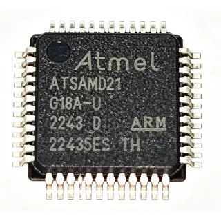
ATSAMD21G15B-AU - 48MHz Cortex-M0+ MCU, 32KB Flash | Microchip
MPN: ATSAMD21G15B-AU ✓ 啟用中ATSAMD21G15B-AU 概覽
A microcontroller (MCU) is a single-chip computer that integrates a CPU core, program and data memory, peripherals, and I/O on one silicon die. The ARM Cortex-M0+ is the smallest and most energy-efficient member of the Cortex-M family, designed for low-power embedded applications such as IoT endpoints, sensor hubs, and battery-powered consumer products. The ATSAMD21G15B-AU extends the Cortex-M0+ instruction set with Thumb-2, hardware multiply, and the optional Microchip SleepWalking peripheral gating scheme, positioning it above 8-bit MCUs in code density while keeping active current in the tens of microamperes per MHz.
Key features include 32 KB Flash plus 4 KB SRAM, six SERCOM channels each reconfigurable as UART, SPI, I2C, or I2S, a built-in full-speed USB 2.0 device transceiver requiring only external pull-up and decoupling, six 16-bit Timer/Counters, and a 12-bit 350 ksps successive-approximation ADC with up to 14 analog channels. Additional features include a 10-bit 350 ksps DAC, two analog comparators, a Real-Time Clock, a 32 kHz low-power oscillator, and an Event System that lets peripherals signal each other without CPU wake-up. The 48-pin TQFP (7x7) package exposes up to 38 GPIO, all 5 V tolerant in input mode, simplifying interfacing to legacy 5 V logic.
At the architecture level, the device pairs the Cortex-M0+ core with a single-cycle hardware multiplier and a Nested Vectored Interrupt Controller (NVIC) supporting 32 IRQ lines. The 48 MHz main clock is sourced from an internal 8 MHz oscillator multiplied by a 48 MHz Digital Frequency-Locked Loop (DFLL48M) with optional 48 MHz to 96 MHz Fractional Digital Phase-Locked Loop (FDPLL96M) for USB jitter compliance. Brown-Out Detection, Power-On Reset, and a Watchdog Timer with independent window safeguard firmware execution, while a separate 32 kHz domain powers SleepWalking and RTC functions without waking the CPU.
Typical applications include consumer wearables, USB HID peripherals, IoT sensor nodes, low-cost home automation, motor-control signal conditioning, and industrial Human-Machine Interface (HMI) panels. Designers choose this part when they need the code density of Cortex-M0+ plus full-speed USB and touch-capable I/O at the smallest flash count of the SAM D21 lineup, accepting that larger firmware requires migration to the G16B or G17L pin-compatible family members.
A practical design consideration: this part is pin-compatible with the rest of the SAM D20/D21 G-series, so PCB footprints, decoupling networks, and SWD headers designed for a 48-pin TQFP can be reused across the family. When evaluating 32 KB against 64 KB flash variants, plan a firmware growth margin up front to avoid last-cycle respins.
This page synthesizes distributor pricing, same-brand drop-in alternatives, and practical design notes not found in the manufacturer datasheet, giving engineers a one-stop view for sourcing, comparison, and PCB migration decisions.
直接替換替代品,適用於 ATSAMD21G15B-AU — 相同封裝,腳位對腳位相容。需重新設計 PCB 的不同封裝零件不列入。
此系列的變體
與下列產品可直接替換的同系列型號: ATSAMD21G15B-AU (相同外形與佔位) — 差異在於 Package, ADC, DAC, Operating Temperature, USB.
ATSAMD21G15B-AUT
✅ 直接替換聯絡詢價
查看資料表 →ATSAMD21G16B-AU
✅ 直接替換聯絡詢價
查看資料表 →ATSAMD21G15B-AF
✅ 直接替換聯絡詢價
查看資料表 →ATSAMD21G16B-AFT
✅ 直接替換聯絡詢價
查看資料表 →ATSAMD20G15A-AU
✅ 直接替換聯絡詢價
查看資料表 →ATSAMD21G17L-AU
✅ 直接替換📋 參考替代品(不在目錄中)
ATSAMD21G15B-AU 最大額定值與電氣特性
| Core | ARM Cortex-M0+ (32-bit) |
| Maximum CPU Clock | 48 MHz |
| Flash Memory | 32 KB (32K x 8) |
| SRAM | 4 KB |
| 封裝 | 48-pin TQFP (7x7 mm) |
| 工作溫度 | -40C to +85C (Industrial) |
| Supply Voltage (VDDIN) | 1.62 V to 3.63 V |
| GPIO | Up to 38 (5 V tolerant inputs) |
| ADC | 12-bit, up to 350 ksps, 14 channels |
| DAC | 10-bit, 350 ksps, 1 channel |
| USB | USB 2.0 Full-Speed Device, integrated transceiver |
| SERCOM | 6 (configurable UART/SPI/I2C/I2S) |
| Timer/Counters | 6 x 16-bit TC, 1 x 24-bit TCC |
| DMA Channels | 12 |
| Event System Channels | 12 |
| RTC | Yes, 32 kHz domain |
| Analog Comparators | 2 |
| Oscillator | Internal 8 MHz + DFLL48M + FDPLL96M |
| Debug Interface | Serial Wire Debug (SWD), 2-pin |
| RoHS 狀態 | Compliant (Green) |
ATSAMD21G15B-AU 腳位配置
| 腳位 1 | PA00 — GPIO / XIN32 (32 kHz crystal input) |
| 腳位 2 | PA01 — GPIO / XOUT32 (32 kHz crystal output) |
| 腳位 3 | PA02 — GPIO / AIN0 (ADC input) |
| 腳位 4 | PA03 — GPIO / AIN1 / VREFA |
| 腳位 5 | GND — Ground |
| 腳位 6 | VDDIO — Digital I/O supply voltage |
| 腳位 7 | PA04 — GPIO / AIN2 |
| 腳位 8 | PA05 — GPIO / AIN3 |
| 腳位 9 | PA06 — GPIO / AIN4 |
| 腳位 10 | PA07 — GPIO / AIN5 |
| 腳位 11 | PA08 — GPIO / NMI |
| 腳位 12 | PA09 — GPIO / I2S MCK1 |
| 腳位 13 | PA10 — GPIO / I2S SCK1 |
| 腳位 14 | PA11 — GPIO / I2S FS1 |
| 腳位 15 | VDDANA — Analog supply voltage |
| 腳位 16 | GND — Ground |
| 腳位 17 | PA12 — GPIO / I2S SDO1 |
| 腳位 18 | PA13 — GPIO / I2S SDI1 |
| 腳位 19 | PA14 — GPIO |
| 腳位 20 | PA15 — GPIO |
| 腳位 21 | PA16 — GPIO / I2S SDO0 / TC4 WO0 |
| 腳位 22 | PA17 — GPIO / I2S SDI0 / TC4 WO1 |
| 腳位 23 | PA18 — GPIO |
| 腳位 24 | PA19 — GPIO |
| 腳位 25 | PA20 — GPIO |
| 腳位 26 | PA21 — GPIO |
| 腳位 27 | PA22 — GPIO / I2S FS0 |
| 腳位 28 | PA23 — GPIO / I2S SCK0 |
| 腳位 29 | PA24 — GPIO / USB D- |
| 腳位 30 | PA25 — GPIO / USB D+ |
| 腳位 31 | PA26 — GPIO |
| 腳位 32 | PA27 — GPIO |
| 腳位 33 | PA28 — GPIO |
| 腳位 34 | PA29 — GPIO / BOOT |
| 腳位 35 | PA30 — GPIO / SWDIO |
| 腳位 36 | PA31 — GPIO / SWCLK |
| 腳位 37 | PB00 — GPIO |
| 腳位 38 | PB01 — GPIO |
| 腳位 39 | PB02 — GPIO / AIN10 |
| 腳位 40 | PB03 — GPIO / AIN11 |
| 腳位 41 | PB04 — GPIO / AIN12 |
| 腳位 42 | PB05 — GPIO / AIN13 |
| 腳位 43 | PB06 — GPIO |
| 腳位 44 | PB07 — GPIO |
| 腳位 45 | PB08 — GPIO |
| 腳位 46 | PB09 — GPIO |
| 腳位 47 | PB10 — GPIO |
| 腳位 48 | PB11 — GPIO |
典型應用
ATSAMD21G15B-AU 適用於 6 應用s: USB HID Consumer Peripherals, Battery-Powered IoT Sensor Nodes, Industrial HMI Control Panels, Wearable Fitness Trackers, Smart Home Edge Sensor Hubs, Educational / Maker Development Boards.
USB HID Consumer Peripherals
The ATSAMD21G15B-AU is a strong fit for USB HID peripherals such as custom keyboards, mice, game controllers, and HID-CDC composite devices because it integrates a full-speed USB 2.0 device transceiver and the 48 MHz FDPLL96M needed to derive the 48 MHz USB reference clock. Designers can implement HID reports over four or five endpoints using the 32 KB Flash and 4 KB SRAM while keeping the BOM minimal, requiring only external pull-up resistors, decoupling capacitors, and a USB-C receptacle. Compared with adding an external USB-to-serial bridge, the integrated approach saves roughly 0.40 USD per board and reduces firmware complexity. The SleepWalking peripherals can wake the core on HID activity, yielding sub-100 microamp standby current on battery-powered game controllers.
推薦
Battery-Powered IoT Sensor Nodes
The ATSAMD21G15B-AU suits battery-powered wireless sensor nodes such as LoRaWAN or Bluetooth beacon peripherals that must operate for years on a coin cell or 2xAA pack. The Event System and SleepWalking peripherals allow the core to stay asleep while ADCs, SERCOMs, and timers gate clocks independently, dropping standby current to single-digit microamperes with full 4 KB SRAM retention. The 12-bit 350 ksps ADC handles periodic sensor reads, and the 6-channel SERCOM supports I2C sensors plus UART debug output. With firmware discipline, designers routinely achieve average current below 20 microamperes in 10 second duty cycles, the threshold where coin-cell batteries last 5+ years.
推薦
Industrial HMI Control Panels
The ATSAMD21G15B-AU drives industrial HMI panels including simple keypads, LED status displays, and small TFT-LCD sub-panels that need debounced GPIO, PWM for backlight dimming, and SERCOM for keypad-scanning I/O expanders. The 48 MHz Cortex-M0+ executes debouncing and LED update algorithms in under 5% CPU load, leaving headroom for serial communication. The 12-bit ADC reads potentiometers or analog sensors on the front panel while the 10-bit DAC generates a reference voltage for sensor excitation. Industrial temperature rating of -40C to +85C ensures operation in factory cabinets with poor ventilation.
推薦
Wearable Fitness Trackers
The ATSAMD21G15B-AU fits wearable fitness bands and step-counter wristbands where small PCB area, low active current, and integrated peripherals matter more than raw Flash size. The Cortex-M0+ executes pedometer state machines and BLE-stack fragments while the SERCOM interfaces an external BLE module or accelerometer such as the LIS2DH over I2C. Designers using SleepWalking with the ADC can sample a heart-rate sensor without waking the CPU, and the 32 KB Flash fits reference pedometer algorithms plus a BLE provisioning flow. The 48-pin TQFP at 7x7 mm pairs with a 2-layer flex PCB typical in wearable designs.
推薦
Smart Home Edge Sensor Hubs
The ATSAMD21G15B-AU acts as a smart-home edge sensor hub aggregating analog sensors, digital switches, and protocol bridges into a single board that talks to a central home automation gateway. The 6 SERCOMs provide UART, SPI, and I2C concurrently to interface sensors and modules, while the integrated USB can enumerate as a CDC device for diagnostics. Combined with the 12-bit ADC and 10-bit DAC, it can read thermistors, drive analog actuators, and pre-process data before forwarding to the gateway, reducing network traffic by 50-80% versus dumb sensor designs.
推薦
Educational / Maker Development Boards
The ATSAMD21G15B-AU is a common microcontroller on educational maker boards (Adafruit ItsyBitsy M0, Arduino MKR-family derivatives) because the 48-pin TQFP exposes enough GPIO for breadboard experiments while staying within student-friendly price points. The integrated USB simplifies programming via the Arduino IDE or Microchip Studio, and the SWD interface lets instructors debug firmware line-by-line. The 32 KB Flash fits reference sketches, BLE-stack fragments, and sensor libraries, while the 6 SERCOMs support common hobby sensors, motors, and displays.
推薦
推薦產品摘要
工程參考資料,適用於 ATSAMD21G15B-AU — 比較、設計指引及合規資訊。
選型指南
與替代品比較
| 參數 | 本產品 | ATSAMD21G15B-AUT | ATSAMD21G16B-AU | ATSAMD21G15B-AF | ATSAMD21G16B-AFT | ATSAMD20G15A-AU | ATSAMD21G17L-AU |
|---|---|---|---|---|---|---|---|
| Brand | Microchip Technology | Microchip Technology | Microchip Technology | Microchip Technology | Microchip Technology | Microchip Technology | Microchip Technology |
| Package | 48-TQFP (7x7 mm) | 48-TQFP (7x7 mm) - same | 48-TQFP (7x7 mm) - same | 48-TQFP (7x7 mm) - same | 48-TQFP (7x7 mm) - same | 48-TQFP (7x7 mm) - same | 48-TQFP (7x7 mm) - same |
| Core / Max Clock | Cortex-M0+ / 48 MHz | Cortex-M0+ / 48 MHz | Cortex-M0+ / 48 MHz | Cortex-M0+ / 48 MHz | Cortex-M0+ / 48 MHz | Cortex-M0+ / 48 MHz | Cortex-M0+ / 48 MHz |
| Flash Memory | 32 KB | 32 KB | 64 KB | 32 KB | 64 KB | 32 KB | 128 KB |
| SRAM | 4 KB | 4 KB | 8 KB | 4 KB | 8 KB | 4 KB | 16 KB |
| Integrated USB 2.0 FS | Yes | Yes | Yes | Yes | Yes | No | Yes |
| DAC / I2S | 10-bit DAC, I2S | 10-bit DAC, I2S | 10-bit DAC, I2S | 10-bit DAC, I2S | 10-bit DAC, I2S | No DAC, no I2S | 10-bit DAC, I2S |
| SleepWalking | Yes (SAM D21) | Yes | Yes | Yes | Yes | No (SAM D20) | Yes |
| Operating Temperature | -40C to +85C | -40C to +85C | -40C to +85C | -40C to +85C | -40C to +85C | -40C to +85C | -40C to +85C |
主要差異化特點
- Integrated USB 2.0 Full-Speed transceiver (對比ATSAMD20G15A-AU)
- Same-family 64 KB Flash upgrade in identical footprint (對比ATSAMD21G16B-AU)
- Cortex-M0+ with SleepWalking peripherals (對比ATSAMD20G15A-AU)
設計說明
Estimated: at 48 MHz CPU clock driving 6 SERCOMs and USB, active current is approximately 7 mA from VDDIO at 3.3 V. For battery-powered designs, configure the Event System so peripherals gate their own clocks using SleepWalking and only interrupt the CPU when needed; this keeps average current below 100 microamperes on a 10-second duty cycle. Decouple VDDIO and VDDANA separately with 100 nF X7R capacitors placed within 5 mm of the respective pins, and place a 4.7 uF bulk capacitor on each rail.
Route the 32 kHz low-frequency crystal traces (PA00 / PA01) as short as possible with both traces matched within 1 mm and a ground pour guard ring around them to avoid injection from switching signals. Route the USB D+/D- pair (PA24 / PA25) as a 90 ohm differential pair with no stubs, keeping the trace length under 50 mm to meet USB 2.0 FS signal-integrity requirements. The exposed thermal pad on the TQFP is not connected to GND internally but should still be soldered to a small copper pour for mechanical rigidity.
Do not leave the SWDIO / SWCLK pins (PA30 / PA31) floating during reset, as the chip samples them to determine boot source; add 100 kohm pull-downs to ensure normal boot from Flash. The brown-out detector (BOD) threshold defaults to 1.85 V at reset, which can be too low for some analog references - raise it to 2.6 V via the FUSE bits during production programming. When migrating from the SAM D20 family, remember the SERCOM pad mapping differs even when pin numbers match; always re-run the Atmel START pin-mux tool.
合規資訊
Microchip product page declares RoHS and REACH compliance (Green compound). Industrial temperature grade -40C to +85C; not AEC-Q100 qualified (no automotive qualification on AU suffix).