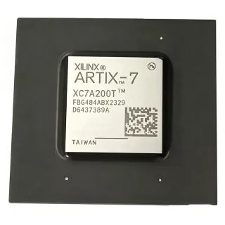
EP4CE30F23I7N - 28,848 LEs, 1.2V Cyclone IV E FPGA | Altera
MPN: EP4CE30F23I7N ✓ 啟用中EP4CE30F23I7N 概覽
An FPGA is a programmable semiconductor in which the logic fabric and configurable input/output resources can be programmed after manufacture. The Cyclone IV E family combines programmable logic blocks, fixed or soft DSP resources, embedded memory, and general-purpose I/O in a single device. This hierarchy places the EP4CE30F23I7N within programmable logic, digital logic ICs, and the broader FPGA and CPLD category.
The device provides 180 logic array blocks according to the Cyclone IV E comparison data, a maximum operating frequency of 200 MHz, and a 1.2 V operating supply. Its 28,848 logic elements support parallel control, protocol handling, data acquisition, and algorithmic pipelines, while 328 user I/O provide connections to external memory, converters, transceivers, sensors, and industrial interfaces. The industrial-grade ordering option supports designs requiring extended-temperature-oriented industrial qualification.
The EP4CE30F23I7N uses an FBGA-484 package, making careful PCB layout essential. Dense ball pitch requires short escape routes, controlled impedance for high-speed interfaces, multiple ground and supply connections, and adequate thermal spreading beneath the device. The package is listed in tray packaging for this ordering configuration.
Typical uses include programmable industrial controllers, camera and image-processing pipelines, communications gateways, motor-control systems, and low-power embedded test equipment. Designers should verify the voltage requirements, pin allocation, configuration method, clocking resources, and supported I/O standards in the manufacturer Cyclone IV E documentation before schematic capture and PCB release.
A key implementation consideration is that FPGA board design is not interchangeable with ordinary fixed-function IC design. Configuration pins, auxiliary supply rails, decoupling, clock jitter tolerance, and JTAG access must be planned together. Keep sensitive interfaces away from high-speed switching nodes and preserve the Cyclone IV E power and ground-plane topology shown in the manufacturer reference material.
This page combines the exact ordering-number attributes, sourcing structure, and practical implementation considerations for engineers evaluating the EP4CE30F23I7N, including package constraints, FPGA-specific design guidance, and clearly qualified replacement analysis.
直接替換替代品,適用於 EP4CE30F23I7N — 相同封裝,腳位對腳位相容。需重新設計 PCB 的不同封裝零件不列入。
此系列的變體
與下列產品可直接替換的同系列型號: EP4CE30F23I7N (相同外形與佔位) — 差異在於 Logic Elements, Package, Core Voltage, RoHS Status, Embedded Memory Bits.
EP4CE30F23I7
✅ 直接替換📋 參考替代品(不在目錄中)
EP4CE30F23C7N
✅ 直接替換聯絡詢價
查看資料表 →EP4CE30F23C7N
✅ 直接替換聯絡詢價
查看資料表 →EP4CE30F23C6
✅ 直接替換📋 參考替代品(不在目錄中)
EP4CE30F23A7N
✅ 直接替換📋 參考替代品(不在目錄中)
EP4CE30F23I7N 最大額定值與電氣特性
| Device Type | Field Programmable Gate Array (FPGA) |
| FPGA Family | Cyclone IV E |
| Logic Elements | 28,848 logic elements |
| Logic Array Blocks | 180 LABs |
| User I/O Pins | 328 I/O pins |
| Package Type | FBGA-484 |
| Total Package Pins | 484 pins |
| 工作電源電壓 | 1.2 V |
| Maximum Operating Frequency | 200 MHz |
| Product Type | FPGA - Field Programmable Gate Array |
| Temperature Grade | Industrial grade |
| 安裝類型 | Surface mount |
| Packaging | Tray |
| Moisture Sensitivity | Moisture sensitive |
| Factory Pack Quantity | 60 units |
| Subcategory | Programmable Logic ICs |
EP4CE30F23I7N 484 pins 腳位配置指南
EP4CE30F23I7N(484 pins 封裝)的腳位配置。 此數位 IC 包含 GPIO、通訊介面(UART、SPI、I2C)與電源腳位。替代腳位功能與配置選項請參閱製造商資料表。對嵌入式系統設計與 PCB 佈局至關重要。

無詳細腳位定義資料: EP4CE30F23I7N.
請參閱 資料表 以查看完整腳位配置。
典型應用
EP4CE30F23I7N 適用於 6 應用s: Industrial Automation Controller, Communications Gateway, Data Acquisition and Signal Processing, Motor Control and Power Management, Video and Image Processing Pipeline, Embedded Test and Measurement.
Industrial Automation Controller
The EP4CE30F23I7N fits industrial automation controllers that coordinate sensors, actuators, interlocks, and machine sequencing. Its 28,848 logic elements and 180 logic array blocks provide substantial parallel processing capacity, while 328 I/O allow multiple digital interfaces to coexist on one controller. The 200 MHz maximum operating frequency supports event-driven and moderately timed control logic. Use the industrial-grade ordering option for suitable temperature requirements, and isolate external field wiring to protect the FPGA from industrial transients and ground potential differences.
推薦
Communications Gateway
The EP4CE30F23I7N can implement protocol conversion, packet framing, and interface bridging in communications equipment. Its 180 logic array blocks allow parallel datapaths to be combined with finite-state-machine control, while 328 I/O provide connectivity for serial links, status signals, and memory interfaces. The 1.2 V core architecture suits modern digital subsystems, but the board must separate high-speed transceiver supplies from FPGA core rails and follow Cyclone IV E decoupling and grounding guidance.
推薦
Data Acquisition and Signal Processing
The EP4CE30F23I7N is suitable for data-acquisition front ends that combine parallel sampling, digital filtering, buffering, and control functions in one programmable device. Its 28,848 logic elements can implement fixed-latency pipelines or parallel processing stages, and 328 I/O supports converters, memory devices, triggers, and synchronization signals. At a 200 MHz maximum operating frequency, timing closure and I/O standards must be checked against the selected Cyclone IV E speed grade and external component timing.
推薦
Motor Control and Power Management
The EP4CE30F23I7N can serve as the digital control core for motor drives, power-conversion equipment, and sequencing systems. Parallel logic resources support PWM generation, fault handling, current-command processing, and communication protocols, while the 328 I/O pins permit simultaneous connection to gate drivers, position sensors, and supervisory controllers. The FPGA does not directly solve analog power-stage requirements, so current sensing, isolation, gate-drive timing, and fail-safe behavior must be validated separately.
推薦
Video and Image Processing Pipeline
The EP4CE30F23I7N can implement parallel image acquisition, pixel manipulation, thresholding, and interface conversion where a fixed-function processor would be less flexible. The 28,848 logic elements support concurrent pipelines, while 328 I/O provide connections for image sensors, memory, and downstream processing devices. Practical deployments must ensure that supported I/O standards, clocking resources, and external memory timing match the design; otherwise, additional interface devices or a higher-density FPGA may be required.
推薦
Embedded Test and Measurement
The EP4CE30F23I7N is well suited to programmable test logic because its logic fabric can implement timing generators, sequencing engines, pattern processors, and communication adapters. Its 1.2 V core supply and 200 MHz maximum operating frequency support digital logic up to the limits established by the selected speed grade and I/O configuration. The FBGA-484 package is appropriate for dense instrumentation, but test-equipment designs should carefully budget power, thermal performance, clock jitter, and differential I/O implementation.
推薦
推薦產品摘要
工程參考資料,適用於 EP4CE30F23I7N — 比較、設計指引及合規資訊。
選型指南
與替代品比較
| 參數 | 本產品 |
|---|---|
| Package | FBGA-484 |
| Brand | Altera |
| FPGA Family | Cyclone IV E |
| Logic Elements | 28,848 |
| Logic Array Blocks | 180 LABs |
| User I/O Pins | 328 I/O pins |
| Operating Supply Voltage | 1.2 V |
| Maximum Operating Frequency | 200 MHz |
| Temperature Grade | Industrial grade |
| Factory Pack Quantity | 60 units |
| Mounting Type | Surface mount |
| Moisture Sensitivity | Moisture sensitive |
主要差異化特點
- High logic capacity within the Cyclone IV E F23 device (對比EP4CE30F23C7N)
- Dense connectivity in a single FBGA-484 device (對比EP4CE30F23C8)
- Industrial-oriented ordering configuration (對比EP4CE30F23A7N)
設計說明
Design the FBGA-484 escape routing and power distribution from the manufacturer package drawing rather than estimating pad geometry. Keep high-speed nets short and continuous, provide multiple connections to the appropriate ground and supply planes, and place decoupling capacitors close to their intended power pins. The 484-pin package requires multilayer-board planning, and a manufacturing-capable design should be checked for via-in-pad, solder-mask, and assembly requirements before release.
Treat the 1.2 V core supply as one part of a complete FPGA power tree. Configuration, I/O banks, auxiliary rails, and external interface devices may require separate voltage planning. Derive worst-case current from the selected Cyclone IV E resource utilization and operating mode, then apply the manufacturer sequencing guidance. Add sufficient bulk and high-frequency decoupling and verify startup behavior across the expected input-voltage range before schematic sign-off.
Estimate the FBGA junction-temperature rise from total FPGA dissipation, board thermal resistance, airflow, and the temperature grade. Start with a conservative thermal budget using the actual logic, memory, and I/O utilization because published maximum frequency alone does not define real operating power. Use copper spreading under the package where the board stack-up permits it and monitor the design at the highest expected ambient temperature. Any estimate should remain separate from manufacturer performance limits.
Use the Cyclone IV E I/O standards, timing constraints, and board-design guidelines to select termination, series resistance, and topology. Account for clock jitter, skew, package delay, and external-interface timing rather than relying only on the 200 MHz device frequency. Keep sensitive clocks and interfaces away from switching nodes, and validate edge rates, return paths, and impedance-controlled structures with the intended PCB stack-up.
合規資訊
The available product information identifies the device as industrial grade but does not provide explicit RoHS, REACH, lead-free, halogen-free, or conflict-minerals statements.