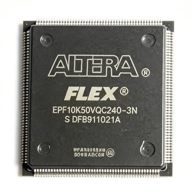
EPF10K50VQC240-3N - FLEX 10K 50K Gates FPGA | Intel / Altera
MPN: EPF10K50VQC240-3N ✗ 停產| 數量 | 單價 | 小計 |
|---|---|---|
| 1 | $78.5 | $78.50 |
| 10 | $70.4 | $704.00 |
| 100 | $61.2 | $6,120.00 |
| 250 | $55.8 | $13,950.00 |
| 500 | $49.95 | $24,975.00 |
EPF10K50VQC240-3N 概覽
An FPGA (Field Programmable Gate Array) is a semiconductor device built from an array of configurable logic elements (LEs), programmable interconnect, and I/O blocks that the user defines after manufacture via a hardware description language (HDL) or schematic capture. The FLEX 10K family was the industry's first family to embed large SRAM-style logic blocks together with dedicated Embedded Array Blocks (EABs), enabling on-chip implementation of megafunctions such as RAM, ROM, and arithmetic units, and it is widely considered the predecessor of modern System-on-Programmable-Chip (SOPC) architectures. The EPF10K50VQC240-3N belongs to the high-density FLEX 10K tier (10K50), differentiating it from lower-density siblings such as the EPF10K10 and EPF10K30.
Key differentiating features include: 20,480 typical gate count, integrated EABs for on-chip memory, in-system programmability via the Serial Configuration (Passive) or Active serial modes supported by the FLEX 10K architecture, multi-voltage I/O compatibility with 5.0 V, 3.3 V, and 2.5 V signalling, and JTAG-compliant boundary-scan test per IEEE 1149.1. The device integrates seamlessly with the legacy MAX+PLUS II and Quartus design tool flows, preserving design IP across older Altera ecosystems.
Technically, the EPF10K50VQC240-3N uses SRAM configuration cells and requires external configuration memory on every power-up. Its configurable logic blocks (CLBs) feed into Embedded Array Blocks (EABs) that deliver up to 2,048 bits of dual-port RAM per block, while the high-pin-count PQFP240 footprint exposes ample general-purpose I/O for parallel bus and memory interfaces.
Typical applications include legacy telecom interface cards, industrial control and factory automation controllers, glue-logic replacement, mid-speed DSP co-processing, and PCI/ISA bus interface prototyping. Engineers commonly select this part to extend the lifecycle of older Altera designs without performing full re-qualification.
When designing with this device, ensure that configuration memory and JTAG pull-up resistors are placed within 5 cm of the device to meet the configuration timing specifications. Designers should also verify that I/O signalling levels match the chosen I/O standard (3.3 V LVTTL/LVCMOS by default) and provide a clean 3.3 V core supply with adequate decoupling. Because this part is in the legacy FLEX 10K family, lead-time and lifecycle risks should be reviewed against the Intel Product Discontinuance Program notice before NPI qualification.
This page synthesises distributor pricing, same-family drop-in alternatives, and practical design notes that go beyond the manufacturer's PDF datasheet alone, giving engineers and buyers a single authoritative reference for the EPF10K50VQC240-3N.
直接替換替代品,適用於 EPF10K50VQC240-3N — 相同封裝,腳位對腳位相容。需重新設計 PCB 的不同封裝零件不列入。
此系列的變體
與下列產品可直接替換的同系列型號: EPF10K50VQC240-3N (相同外形與佔位) — 差異在於 Series, Speed Grade, Configuration Method, Operating Temperature, Process Technology.
快速比較工具 — 選擇替代零件進行並排比較:
EPF10K50VQC240-2N
聯絡詢價
查看資料表 →EPF10K50VQC240-2
聯絡詢價
查看資料表 →EPF10K50VQC240-1N
聯絡詢價
查看資料表 →EPF10K50VQC240-1
聯絡詢價
查看資料表 →EPF10K30AQC240-3
聯絡詢價
查看資料表 →EPF10K50VQC240-3N 最大額定值與電氣特性
| Family | FLEX 10K |
| Series | FLEX 10K |
| Logic Cells / Elements | 2880 |
| Total RAM Bits | 20480 |
| Number of LABs/CLBs | 360 |
| Number of User I/Os | 189 |
| System Gates | 50000 |
| Internal Frequency (max) | 125 MHz |
| Propagation Delay | 0.6 ns |
| 工作電源電壓 | 3.3 V |
| Technology | 0.42 µm CMOS |
| 工作溫度 | 0 °C to +70 °C (Commercial) |
| 安裝類型 | Surface Mount |
| 封裝 | 240-BFQFP / PQFP |
| Speed Grade | -3 |
| Compliance / Lead Status | Contains lead; verify RoHS applicability per lot |
EPF10K50VQC240-3N 240-bfqfp / pqfp 腳位配置指南
EPF10K50VQC240-3N(240-bfqfp / pqfp 封裝)的腳位配置。 此數位 IC 包含 GPIO、通訊介面(UART、SPI、I2C)與電源腳位。替代腳位功能與配置選項請參閱製造商資料表。對嵌入式系統設計與 PCB 佈局至關重要。

無詳細腳位定義資料: EPF10K50VQC240-3N.
請參閱 資料表 以查看完整腳位配置。
典型應用
EPF10K50VQC240-3N 適用於 6 應用s: Legacy Telecom Interface Card Glue Logic, Industrial Control and Factory Automation Controller, Glue Logic Replacement on Motherboards, Mid-Speed DSP Co-Processing Engine, PCI / ISA Bus Interface Prototyping, Test and Measurement Instrumentation Front-End.
Legacy Telecom Interface Card Glue Logic
The EPF10K50VQC240-3N fits legacy telecom interface cards that require medium-density glue logic with PCI/ISA bus bridging. Its 189 user I/Os and 50K system gates provide ample capacity to aggregate multiple bus interfaces, while the 3.3 V supply and 0.6 ns propagation delay support 33 MHz PCI timing. The PQFP240 package exposes enough pins for parallel data buses plus bus arbitration, and the embedded SRAM blocks (EABs) can implement FIFOs for packet buffering at T1/E1 line rates. Engineers select this part to extend the lifecycle of installed telecom base without redesigning around modern Cyclone devices.
推薦
Industrial Control and Factory Automation Controller
The EPF10K50VQC240-3N is well-suited to industrial PLC and motion-control cards that need 50K gates of deterministic glue logic between a microcontroller and I/O. Its 360 LABs and 189 I/Os let designers instantiate multiple encoder counters, PWM blocks, and serial protocol bridges (RS-485, CAN) inside one chip. The commercial 0-70 °C operating range covers most factory-floor enclosures, while the 240-PQFP package is mechanically robust for vibration-prone installations. The part's NRND status makes it ideal for sustaining legacy automation lines that already have qualified FLEX 10K firmware flows in production.
推薦
Glue Logic Replacement on Motherboards
The EPF10K50VQC240-3N replaces discrete 74-series TTL and PAL/GAL devices on older VME and cPCI motherboards where a single FPGA consolidates address decoding, interrupt control, and bus arbitration. Its 189 user I/Os comfortably absorb 32-bit address plus 32-bit data plus control signals, while the on-chip EABs implement wait-state generators. The 3.3 V core with multi-voltage I/O supports legacy 5 V peripherals through level-shifted banks. Designers benefit from reduced board area and BOM count versus discrete logic.
推薦
Mid-Speed DSP Co-Processing Engine
The EPF10K50VQC240-3N serves as a co-processor for mid-speed DSP workloads such as FIR filters, FFT pre-processing, and video line buffers in surveillance and instrumentation equipment. Its 50K gates plus 20,480 bits of EAB RAM provide dual-port memory blocks ideal for sample buffering at 30-50 MHz sample rates. The 125 MHz internal Fmax supports multiply-accumulate loops at audio and low-end video bandwidths. The PQFP240 package exposes dedicated clock and global buffer pins needed for synchronous DSP chains.
推薦
PCI / ISA Bus Interface Prototyping
The EPF10K50VQC240-3N is widely used to prototype PCI and ISA bus interface cores where the FPGA implements target or master logic with 32-bit/33 MHz PCI compliance. The 189 I/Os are sufficient for a multiplexed PCI bus plus auxiliary control, and the on-chip RAM enables zero-wait-state burst transfers. Engineers use the MAX+PLUS II or Quartus II toolchains to integrate verified PCI MegaCore functions and iterate on glue logic. The PQFP240 footprint is compatible with numerous PCI evaluation boards from the late 1990s and early 2000s.
推薦
Test and Measurement Instrumentation Front-End
The EPF10K50VQC240-3N is used in legacy oscilloscope, logic analyser, and protocol analyser front-ends where 50K gates of custom trigger logic and 189 I/Os are needed to fan-out high-speed parallel sample buses. Its embedded EABs implement deep sample FIFOs that buffer pre-trigger data before software read-back, while the deterministic 0.6 ns propagation delay supports precise timing-arm logic. The commercial operating range and robust PQFP240 package suit benchtop instruments that have been in field service for 15+ years.
推薦
推薦產品摘要
工程參考資料,適用於 EPF10K50VQC240-3N — 比較、設計指引及合規資訊。
選型指南
與替代品比較
| 參數 | 本產品 | EPF10K50VQC240-3 | EPF10K50VQC240-2N | EPF10K50VQC240-2 | EPF10K50VQC240-1N | EPF10K50VQC240-1 | EPF10K30AQC240-3 |
|---|---|---|---|---|---|---|---|
| Brand | Intel (formerly Altera) | Intel | Intel | Intel | Intel | Intel | Intel |
| Package | 240-PQFP (VQC240) | 240-PQFP - same | 240-PQFP - same | 240-PQFP - same | 240-PQFP - same | 240-PQFP - same | 240-PQFP - same |
| Family | FLEX 10K | FLEX 10K | FLEX 10K | FLEX 10K | FLEX 10K | FLEX 10K | FLEX 10KA |
| Speed Grade | -3 | -3 | -2 (slower) | -2 (slower) | -1 (slowest) | -1 (slowest) | -3 |
| System Gates | 50000 | 50000 | 50000 | 50000 | 50000 | 50000 | 30000 (-40%) |
| Logic Cells / Elements | 2880 | 2880 | 2880 | 2880 | 2880 | 2880 | 1728 |
| User I/Os | 189 | 189 | 189 | 189 | 189 | 189 | 189 |
| Operating Voltage | 3.3 V | 3.3 V | 3.3 V | 3.3 V | 3.3 V | 3.3 V | 3.3 V |
| Pb-free / RoHS | Yes (N suffix) | No (legacy lead) | Yes | No | Yes | No | No |
| Process | 0.42 µm CMOS | 0.42 µm | 0.42 µm | 0.42 µm | 0.42 µm | 0.42 µm | 0.30 µm (newer) |
主要差異化特點
- Fastest speed grade (-3) in the FLEX 10K 10K50 PQFP240 family (對比EPF10K50VQC240-2N)
- Pb-free / RoHS-compliant lead finish (N suffix) (對比EPF10K50VQC240-3)
- 50K system gates versus 30K in the FLEX 10KA sibling (對比EPF10K30AQC240-3)
設計說明
The EPF10K50VQC240-3N requires a clean 3.3 V core supply. Estimated: at typical Icc of approximately 200-300 mA during user-mode operation plus in-rush during configuration, design a 3.3 V regulator rated for at least 500 mA with 10 µF bulk + 0.1 µF ceramic decoupling placed within 25 mm of every VCC pin pair. Add a 1 µF tantalum at the device's power pin if the upstream rail exceeds 30 cm of trace. Always decouple both core VCCINT and I/O VCCIO banks separately because the FLEX 10K architecture powers them independently.
Configuration memory (typically EPC2 or EPC16) and JTAG pull-up resistors must be placed within 50 mm of the EPF10K50VQC240-3N to meet configuration timing. For Passive Serial configuration mode, the DCLK trace length must not exceed the data setup/hold specification; for Active Serial mode, route DCLK and DATA0 as a length-matched pair. The PQFP240 footprint requires adequate breakaway/panelisation clearance because the 0.5 mm pitch gull-wing leads demand precise paste-stencil apertures of approximately 0.20 mm × 1.6 mm.
The 'N' suffix indicates Pb-free / RoHS-compliant lead finish; the no-suffix version contains lead and may not be acceptable for current RoHS markets. Designers migrating legacy designs must verify whether their BOM was qualified against the lead-finish variant before swapping. Also note that Quartus versions newer than 13.0sp1 do not support FLEX 10K device compilation - older design flows must be preserved on the MAX+PLUS II / Quartus II 13.0sp1 toolchain to regenerate bitstreams. NRND status means new NPI designs should target Cyclone IV/V instead.
Because the EPF10K50VQC240-3N drives 189 user I/Os on a large PQFP240 package, signal-integrity planning is essential at edges above 50 MHz. Series-damping resistors (22-33 Ω) on critical clocks and source-synchronous data help reduce overshoot on the 0.5 mm-pitch lead frame. Maintain a continuous ground plane under the package and stitch VCC/GND with vias on a 5 mm grid around the PQFP body. For 3.3 V LVTTL outputs driving 5 V TTL receivers, verify that Vih_min is satisfied - the FLEX 10K VCCIO bank voltage determines the output VIH/VOH levels per the device handbook.
合規資訊
The 'N' suffix indicates Pb-free lead finish per Altera/Intel legacy package specification. RoHS and REACH compliance inferred from Pb-free N-suffix designation and Intel/Altera legacy product environmental statements; no individual lot certificate was located in the Verified Web Data. Halogen-free and conflict-minerals status not stated in available sources and marked unknown per Data Authenticity Rule 2.






