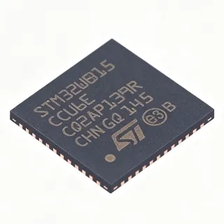
IW611UK-A1IZ - Wi-Fi 6 + BT 5.4 RF Transceiver | NXP
MPN: IW611UK-A1IZ ✓ 啟用中IW611UK-A1IZ 概覽
A Wi-Fi/Bluetooth combo transceiver is a type of RF IC that integrates a radio modem, baseband, and MAC functions for multiple wireless protocols in one die. It sits at the connectivity layer of the system hierarchy: RF transceiver -> wireless connectivity IC -> RF and wireless semiconductor -> semiconductor device. Combo ICs reduce bill-of-materials, board area, and RF coexistence complexity compared with two separate radios.
Key features include dual-band 1x1 Wi-Fi 6 support for OFDMA and uplink/downlink MU-MIMO basics of the 802.11ax standard, Bluetooth 5.4 with Bluetooth Low Energy for LE Audio-ready designs, and a high degree of single-chip integration that NXP states contributes to very low system cost. The WLCSP ball grid array keeps the footprint compact for space-limited smart devices.
Technically, the IW611 integrates the full RF front-end path for both 2.4 GHz and 5 GHz bands, sharing an antenna-facing front end with an internal coexistence scheme between Wi-Fi and Bluetooth air interfaces. The 5 GHz receiver covers 5.17 GHz to 5.895 GHz, spanning the UNII-1 through UNII-3 bands used in most regulatory domains.
Typical applications include smart home devices and accessories, smart appliances, smart energy infrastructure, industrial automation nodes, and embedded gateways, where one chip provides both high-throughput Wi-Fi 6 connectivity and BLE for commissioning, beacons, and sensor links.
Design consideration: because this is a bare WLCSP RF device, PCB stack-up, antenna matching, and power-supply filtering must follow the NXP reference design closely; layout errors directly degrade sensitivity and EMI compliance.
This page synthesizes distributor pricing, verified drop-in family alternatives, datasheet sourcing, and practical design guidance not consolidated in the manufacturer datasheet alone.
直接替換替代品,適用於 IW611UK-A1IZ — 相同封裝,腳位對腳位相容。需重新設計 PCB 的不同封裝零件不列入。
此系列的變體
與下列產品可直接替換的同系列型號: IW611UK-A1IZ (相同外形與佔位) — 差異在於 Bluetooth Version, Frequency Bands, Integration Level.
IW611UK-A1ITZ
✅ 直接替換聯絡詢價
查看資料表 →IW611UK-A1IAZ
✅ 直接替換📋 參考替代品(不在目錄中)
IW611UK-A1IZ 規格
| RF Protocol | Wi-Fi 6 (802.11ax) + Bluetooth 5.4 / BLE |
| Frequency Bands | 2.4 GHz and 5 GHz dual-band |
| 5 GHz Receive Range | 5.17 GHz to 5.895 GHz |
| Wi-Fi Configuration | 1x1 (single spatial stream) |
| Bluetooth Version | Bluetooth v5.4 including Bluetooth Low Energy |
| 供應電壓 | 1.8 V to 3.3 V |
| 封裝 | 140-XFBGA, WLCSP |
| 安裝類型 | Surface Mount |
| Integration Level | Single-chip Wi-Fi + Bluetooth combo |
| Target Applications | IoT, smart home, smart appliances, smart energy, industrial automation, gateways |
IW611UK-A1IZ 140-xfbga, wlcsp 腳位配置指南
IW611UK-A1IZ(140-xfbga, wlcsp 封裝)的腳位配置。 腳位編號、功能與連接圖定義於製造商資料手冊中。請參閱該手冊以取得確切的封裝尺寸與焊接指引。

無詳細腳位定義資料: IW611UK-A1IZ.
請參閱 資料表 以查看完整腳位配置。
典型應用
IW611UK-A1IZ 適用於 6 應用s: Smart Home Devices and Accessories, Smart Appliances, Smart Energy Infrastructure, Industrial Automation Nodes, Embedded Gateways, Smart Devices and Wearable Accessories.
Smart Home Devices and Accessories
The IW611UK-A1IZ fits smart home products because it merges dual-band 1x1 Wi-Fi 6 (802.11ax) with Bluetooth 5.4/BLE on one die, cutting BOM count and board area in exactly the way NXP designed it for. BLE handles commissioning, proximity, and sensor links, while Wi-Fi 6 provides cloud connectivity with OFDMA and TWT for lower idle power in always-on accessories. Integrated on a 140-XFBGA WLCSP footprint from a 1.8V to 3.3V supply, it slots into compact product enclosures; the trade-off is stricter RF layout discipline than a module-based design.
推薦
Smart Appliances
For connected washing machines, refrigerators, and ovens, the IW611UK-A1IZ provides the single-chip 2.4/5 GHz Wi-Fi 6 plus Bluetooth 5.4 connectivity NXP targets explicitly for smart appliances. Dual-band operation lets the appliance avoid congested 2.4 GHz networks by using the 5.17 to 5.895 GHz band, improving throughput for status streaming and OTA firmware updates. BLE 5.4 enables local setup from a phone without provisioning a temporary hotspot. Operating from 1.8V to 3.3V matches appliance controller rails, and the high integration level NXP cites lowers total system cost across volume production.
推薦
Smart Energy Infrastructure
NXP positions the IW611 directly for smart energy applications such as meters, gateways, and energy-management endpoints. The IW611UK-A1IZ's dual-band 1x1 Wi-Fi 6 radio delivers the reliable backhaul these endpoints need while OFDMA improves behavior when thousands of meters share spectrum, and Bluetooth Low Energy supports local field-service configuration via a phone or tablet. The 140-XFBGA WLCSP package and 1.8V to 3.3V supply fit compact, cost-sensitive meter electronics. Designers should budget for robust isolation and surge protection around the RF path, since meter environments are electrically harsh compared with consumer products.
推薦
Industrial Automation Nodes
In factory automation, the IW611UK-A1IZ serves wireless sensor nodes, HMI accessories, and machine-monitoring endpoints where NXP explicitly targets industrial automation. Wi-Fi 6's TWT mechanism reduces node power draw between transmissions, and dual-band capability lets integrators place control traffic on the cleaner 5 GHz band (5.17 to 5.895 GHz RX coverage) away from noisy 2.4 GHz shop-floor spectrum. Bluetooth 5.4 gives maintenance staff a local BLE diagnostic channel. The WLCSP package demands careful conformal coating and layout in industrial environments, but yields a compact, integrated connectivity subsystem at low system cost.
推薦
Embedded Gateways
For compact IoT gateways, the IW611UK-A1IZ provides the WAN-side Wi-Fi 6 client or AP capability plus BLE commissioning in a single 2.4/5 GHz chip, exactly the gateway use case NXP cites for the IW611 family. A 1x1 antenna configuration keeps RF front-end cost minimal while 802.11ax OFDMA sustains aggregate traffic from many downstream nodes. The 140-XFBGA WLCSP footprint minimizes gateway PCB area, and the 1.8V to 3.3V input range simplifies integration with gateway power supplies. For throughput-heavy gateways, pair it with a host processor exposing sufficient SDIO/USB bandwidth per the datasheet host-interface specification.
推薦
Smart Devices and Wearable Accessories
Smart devices and their accessories benefit from the IW611UK-A1IZ's high integration: one chip replaces separate Wi-Fi and Bluetooth radios, shrinking the PCB of space-constrained products. NXP lists smart devices and accessories as a primary IW611 market. BLE 5.4 supports LE Audio-ready links and beaconing for phone accessories, while Wi-Fi 6 handles high-rate tasks like media sync and firmware updates over both 2.4 GHz and 5 GHz bands. Designers should place the WLCSP die close to the antenna with controlled-impedance matching, since every millimeter of mismatched trace erodes the link budget of a 1x1 radio.
推薦
推薦產品摘要
工程參考資料,適用於 IW611UK-A1IZ — 比較、設計指引及合規資訊。
選型指南
與替代品比較
| 參數 | 本產品 | IW611UK-A1ITZ | IW611UK-A1IAZ |
|---|---|---|---|
| Package | 140-XFBGA, WLCSP | 140-XFBGA, WLCSP - same | 140-XFBGA, WLCSP - same |
| Brand | NXP Semiconductors | NXP Semiconductors | NXP Semiconductors |
| Wi-Fi Standard | Wi-Fi 6 (802.11ax), 1x1 | Wi-Fi 6 (802.11ax), 1x1 | Wi-Fi 6 (802.11ax), 1x1 |
| Bluetooth Version | Bluetooth 5.4 / BLE | Bluetooth 5.4 / BLE | Bluetooth 5.4 / BLE |
| Frequency Bands | 2.4 GHz + 5 GHz | 2.4 GHz + 5 GHz | 2.4 GHz + 5 GHz |
| Supply Voltage | 1.8 V to 3.3 V | 1.8 V to 3.3 V | 1.8 V to 3.3 V |
| Lifecycle Status | Active | Active | Active |
主要差異化特點
- Wi-Fi 6 (802.11ax) with OFDMA and TWT in a single chip (對比IW611UK-A1ITZ)
- Bluetooth 5.4 / BLE support (對比IW611UK-A1IAZ)
- Very low system cost through high integration (對比Two-chip Wi-Fi + BLE discrete solutions)
設計說明
The IW611UK-A1IZ uses a 140-ball WLCSP (XFBGA) with fine ball pitch. Follow the NXP IW611 datasheet land-pattern and stack-up recommendations exactly: use a controlled-impedance 50-ohm feed from the RF pin to the antenna with a pi-network for matching, keep the matching network within 2-3 mm of the ball, and provide solid, uninterrupted ground planes on the layer directly beneath the die. Via-stitch the ground pour around the RF section to suppress cavity resonances that would degrade 5 GHz sensitivity.
Supply the IW611 within its 1.8V to 3.3V range, but note the chip internally derives multiple rails; per the NXP datasheet power section, provide per-rail decoupling with a bulk 10 uF plus 0.1 uF and 1 nF ceramic组合 per pin group as specified in the reference design. Because the RF PA draws burst currents during TX, place the bulk capacitor close to the supply balls and use a regulator with good load transient response; otherwise TX burst noise can couple into shared analog rails.
Do not treat the A1IZ/A1ITZ/A1IAZ suffixes as interchangeable without checking the NXP ordering table; although silicon is identical, qualification and packing variants can differ. Also, WLCSP parts are moisture-sensitive - follow the MSL floor-life rules and bake if exposure limits are exceeded before reflow, or popcorn cracking of the package can occur during soldering.
合規資訊
Compliance status not explicitly stated in retrieved web data; confirm on the NXP IW611UK product page or distributor compliance certificates. As an active consumer/IoT NXP part it is typically RoHS-compliant, but XAIPART does not assume compliance without source data.