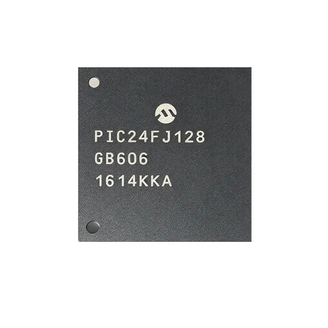
PIC24FJ128GB606-E/MR - 16-Bit 32MHz 128KB Flash USB MCU | Microchip
MPN: PIC24FJ128GB606-E/MR ✗ 停產| 數量 | 單價 | 小計 |
|---|---|---|
| 1 | $6.42 | $6.42 |
| 10 | $5.85 | $58.50 |
| 100 | $5.12 | $512.00 |
| 500 | $4.43 | $2,215.00 |
| 1,000 | $3.78 | $3,780.00 |
PIC24FJ128GB606-E/MR 概覽
A microcontroller (MCU) is a single-chip computer that integrates a CPU core, program memory (Flash), data memory (RAM), peripherals, and I/O into one package. Within the broader semiconductor taxonomy, an MCU belongs to: microcontroller -> embedded processor -> digital IC -> integrated circuit. The PIC24F family uses a 16-bit modified-Harvard architecture with a 24-bit instruction word, providing higher code density than 8-bit MCUs while remaining cost-competitive for embedded designs.
Key features include 128KB (43K x 24) dual-partition Flash with Live Update capability for field-firmware upgrades without downtime, 32KB RAM, integrated USB 2.0 full-speed OTG with PHY, and the eXtreme Low Power (XLP) technology that delivers nanoWatt standby currents below 20 nA in deep sleep. The device provides multiple communication peripherals (UART, SPI, I2C), a 16-channel 10/12-bit ADC, five 16-bit timers, and up to 53 I/O pins.
The architecture supports Peripheral Pin Select (PPS) remappable I/O, allowing flexible PCB routing. The dual-partition Flash with Live Update is engineered for applications that cannot tolerate firmware-update downtime, such as industrial controllers, medical devices, and USB-connected peripherals. Hardware CRC, a real-time clock calendar (RTCC), and a 32kHz secondary oscillator support battery-backed operation.
Typical applications include USB peripherals (Human Interface Devices, mass storage, CDC serial bridges), industrial sensor hubs, automotive body and infotainment subsystems, portable medical/fitness devices, low-power IoT edge nodes, and consumer electronics with USB connectivity and firmware-update requirements.
When designing with this MCU, choose decoupling per Microchip's application note AN584 (typically 100 nF + 10 uF near each supply pin), and ensure the exposed thermal pad is soldered to a sufficient copper pour to meet the package thermal resistance. The Live Update feature requires dual-image flash partitioning in linker configuration.
This page synthesizes distributor pricing, drop-in compatible alternatives from the PIC24FJ family, and practical design notes not consolidated in the manufacturer datasheet.
直接替換替代品,適用於 PIC24FJ128GB606-E/MR — 相同封裝,腳位對腳位相容。需重新設計 PCB 的不同封裝零件不列入。
此系列的變體
與下列產品可直接替換的同系列型號: PIC24FJ128GB606-E/MR (相同外形與佔位) — 差異在於 Package, I/O Pins, ADC, Core Architecture, MSL Level.
快速比較工具 — 選擇替代零件進行並排比較:
PIC24FJ128GA606-E/MR
聯絡詢價
查看資料表 →PIC24FJ128GB406-I/MR
聯絡詢價
查看資料表 →PIC24FJ128GA006-I/MR
聯絡詢價
查看資料表 →PIC24FJ128DA106-I/MR
聯絡詢價
查看資料表 →PIC24FJ1024GA606-I/MR
聯絡詢價
查看資料表 →PIC24FJ1024GB606-I/MR
📋 參考替代品(不在目錄中)
PIC24FJ128GB606-E/MR 最大額定值與電氣特性
| Core | PIC24F (16-bit RISC modified-Harvard) |
| CPU Architecture | 16-bit data, 24-bit instruction word |
| Maximum CPU Frequency | 32 MHz |
| Program Memory (Flash) | 128 KB (43K x 24) dual-partition with Live Update |
| RAM | 32 KB |
| Operating Voltage (Vcc/Vdd) | 2.0 V to 3.6 V |
| I/O Pins | Up to 53 |
| 封裝 | 64-pin VQFN (MR) 9x9 mm with exposed pad |
| 安裝類型 | Surface Mount |
| USB Interface | USB 2.0 Full-Speed OTG with on-chip PHY |
| ADC | 10/12-bit, up to 16 channels |
| Timers | Five 16-bit timers/counters |
| Communication Peripherals | UART, SPI, I2C, PMP, RTCC |
| 工作溫度 | -40 C to +125 C (E grade) |
| AEC-Q100 Qualification | Yes |
| RoHS 狀態 | ROHS3 Compliant |
| MSL 等級 | 3 (168 hours, floor life) |
PIC24FJ128GB606-E/MR 腳位配置
| 腳位 1 | RP5/RB5 — Remappable I/O / Port B bit 5 |
| 腳位 2 | RP6/RB6 — Remappable I/O / Port B bit 6 |
| 腳位 3 | RP7/RB7 — Remappable I/O / Port B bit 7 |
| 腳位 4 | RP8/RB8 — Remappable I/O / Port B bit 8 |
| 腳位 5 | RP9/RB9 — Remappable I/O / Port B bit 9 |
| 腳位 6 | VSS — Ground |
| 腳位 7 | VDD — Positive supply voltage |
| 腳位 8 | RP10/RB10 — Remappable I/O / Port B bit 10 |
| 腳位 9 | RP11/RB11 — Remappable I/O / Port B bit 11 |
| 腳位 10 | RP12/RB12 — Remappable I/O / Port B bit 12 |
| 腳位 11 | RP13/RB13 — Remappable I/O / Port B bit 13 |
| 腳位 12 | RP14/RB14 — Remappable I/O / Port B bit 14 |
| 腳位 13 | OSC1/RC12 — Crystal oscillator input / Port C bit 12 |
| 腳位 14 | OSC2/RC13 — Crystal oscillator output / Port C bit 13 |
| 腳位 15 | SOSCO/RC14 — Secondary oscillator output / RTCC |
| 腳位 16 | SOSCI/RC15 — Secondary oscillator input / RTCC |
| 腳位 17 | VSS — Ground |
| 腳位 18 | VDD — Positive supply voltage |
| 腳位 19 | MCLR — Master clear (reset) input |
| 腳位 20 | PGED2/RP20 — Programming data line 2 / Remappable I/O |
| 腳位 21 | PGEC2/RP21 — Programming clock line 2 / Remappable I/O |
| 腳位 22 | PGED1/RP22 — Programming data line 1 / Remappable I/O |
| 腳位 23 | PGEC1/RP23 — Programming clock line 1 / Remappable I/O |
| 腳位 24 | VSS — Ground |
| 腳位 25 | VDD — Positive supply voltage |
| 腳位 26 | RP24/RD0 — Remappable I/O / Port D bit 0 |
| 腳位 27 | RP25/RD1 — Remappable I/O / Port D bit 1 |
| 腳位 28 | RP26/RD2 — Remappable I/O / Port D bit 2 |
| 腳位 29 | RP27/RD3 — Remappable I/O / Port D bit 3 |
| 腳位 30 | D+ — USB D+ data line |
| 腳位 31 | D- — USB D- data line |
| 腳位 32 | VBUS — USB VBUS detect |
| 腳位 33 | VUSB3V3 — USB internal 3.3V regulator output |
| 腳位 34 | RP28/RD4 — Remappable I/O / Port D bit 4 |
| 腳位 35 | RP29/RD5 — Remappable I/O / Port D bit 5 |
| 腳位 36 | RP30/RD6 — Remappable I/O / Port D bit 6 |
| 腳位 37 | RP31/RD7 — Remappable I/O / Port D bit 7 |
| 腳位 38 | VSS — Ground |
| 腳位 39 | VDD — Positive supply voltage |
| 腳位 40 | RP0/RB0 — Remappable I/O / Port B bit 0 |
| 腳位 41 | RP1/RB1 — Remappable I/O / Port B bit 1 |
| 腳位 42 | RP2/RB2 — Remappable I/O / Port B bit 2 |
| 腳位 43 | RP3/RB3 — Remappable I/O / Port B bit 3 |
| 腳位 44 | RP4/RB4 — Remappable I/O / Port B bit 4 |
| 腳位 45 | AN0/RA0 — Analog input 0 / Port A bit 0 |
| 腳位 46 | AN1/RA1 — Analog input 1 / Port A bit 1 |
| 腳位 47 | AN2/RA2 — Analog input 2 / Port A bit 2 |
| 腳位 48 | AN3/RA3 — Analog input 3 / Port A bit 3 |
| 腳位 49 | AN4/RA4 — Analog input 4 / Port A bit 4 |
| 腳位 50 | AN5/RA5 — Analog input 5 / Port A bit 5 |
| 腳位 51 | VREF-/RA6 — ADC negative reference / Port A bit 6 |
| 腳位 52 | VREF+/RA7 — ADC positive reference / Port A bit 7 |
| 腳位 53 | VSS — Ground |
| 腳位 54 | VDD — Positive supply voltage |
| 腳位 55 | RC1/AN6 — Port C bit 1 / Analog input 6 |
| 腳位 56 | RC2/AN7 — Port C bit 2 / Analog input 7 |
| 腳位 57 | RC3/AN8 — Port C bit 3 / Analog input 8 |
| 腳位 58 | RC4/AN9 — Port C bit 4 / Analog input 9 |
| 腳位 59 | RP15/RB15 — Remappable I/O / Port B bit 15 |
| 腳位 60 | RP16/RC0 — Remappable I/O / Port C bit 0 |
| 腳位 61 | RP17/RC5 — Remappable I/O / Port C bit 5 |
| 腳位 62 | RP18/RC6 — Remappable I/O / Port C bit 6 |
| 腳位 63 | RP19/RC7 — Remappable I/O / Port C bit 7 |
| 腳位 64 | VSS — Ground (exposed thermal pad) |
典型應用
PIC24FJ128GB606-E/MR 適用於 6 應用s: USB Human Interface Device (HID), Industrial Sensor Hub, Automotive Body Control Module, Portable Medical / Fitness Device, IoT Edge Node with USB Provisioning, USB Mass Storage / CDC Bridge.
USB Human Interface Device (HID)
The PIC24FJ128GB606-E/MR is purpose-built for USB HID peripherals such as keyboards, mice, game controllers, and custom input devices. Its integrated USB 2.0 full-speed OTG controller with on-chip PHY eliminates external PHY components, reducing BOM cost and PCB area. The 32MHz CPU and 128KB Flash easily handle HID class descriptors, multi-button debouncing, and firmware-upgrade routines over USB. With AEC-Q100 qualification, the same firmware can ship in consumer and automotive HID variants. Combined with PIC24F XLP sleep modes, battery-powered wireless HID dongles achieve multi-year coin-cell lifetimes.
推薦
Industrial Sensor Hub
In industrial sensor hubs, the PIC24FJ128GB606-E/MR aggregates multiple sensor inputs over I2C, SPI, and UART while providing a USB data uplink to a host PC or PLC. The 16-channel 10/12-bit ADC supports analog sensor digitization, and Peripheral Pin Select remapping simplifies PCB layout when adding sensors. XLP nanoWatt sleep currents (below 20 nA) enable battery-only field deployments with 10+ year lifetimes. Dual-partition Flash with Live Update allows OTA-style firmware updates over USB without halting data acquisition, critical for 24/7 industrial installations.
推薦
Automotive Body Control Module
The PIC24FJ128GB606-E/MR's AEC-Q100 qualification and -40C to +125C operating range make it suitable for automotive body and infotainment subsystems. Typical functions include USB media port control, ambient lighting, mirror modules, and HVAC user interfaces. The PIC24F 16-bit core provides deterministic interrupt latency required for CAN-bridge and LIN-master firmware, while USB OTG enables media playback from USB drives. Live Update allows dealer-level firmware reflashing without ECU downtime, reducing warranty cost.
推薦
Portable Medical / Fitness Device
Battery-powered medical and fitness devices benefit from the PIC24FJ128GB606-E/MR's XLP technology, AEC-Q100 reliability, and USB connectivity for charging and data sync. Heart-rate monitors, pulse oximeters, and smart insulin pens use the 12-bit ADC for analog front-end sampling and the USB OTG port for data upload to mobile apps. NanoWatt sleep modes extend battery life to weeks or months, and the Live Update feature allows firmware updates without disrupting measurement sessions, important for medical-device compliance.
推薦
IoT Edge Node with USB Provisioning
IoT edge nodes using the PIC24FJ128GB606-E/MR leverage USB for factory provisioning and field updates while running low-power sensor duties from battery. The MCU acts as a USB CDC/ECM bridge to Wi-Fi modules, or directly enumerates as a USB device for commissioning tools. Dual-partition Flash with Live Update enables fail-safe OTA updates. The XLP sleep current below 20 nA lets solar or coin-cell-powered sensors operate for years between maintenance windows.
推薦
USB Mass Storage / CDC Bridge
The PIC24FJ128GB606-E/MR is well suited for USB mass storage class devices, CDC serial bridges, and composite USB devices that combine multiple USB functions. The 128KB Flash accommodates USB class drivers plus application logic, and the 32KB RAM handles SCSI/BBB buffering for read/write operations. Full-speed USB (12 Mbps) is sufficient for SD-card readers, EEPROM programmers, and UART-to-USB converters. AEC-Q100 qualification allows the same firmware in automotive diagnostic tools.
推薦
推薦產品摘要
工程參考資料,適用於 PIC24FJ128GB606-E/MR — 比較、設計指引及合規資訊。
選型指南
與替代品比較
| 參數 | 本產品 | PIC24FJ128GA606-E/MR | PIC24FJ128GB406-I/MR | PIC24FJ128GA006-I/MR | PIC24FJ128DA106-I/MR | PIC24FJ1024GB606-I/MR |
|---|---|---|---|---|---|---|
| Brand | Microchip Technology | Microchip Technology | Microchip Technology | Microchip Technology | Microchip Technology | Microchip Technology |
| Package | 64-VQFN (9x9 mm) | 64-VQFN (9x9 mm) - same | 64-VQFN (9x9 mm) - same | 64-VQFN (9x9 mm) - same | 64-VQFN (9x9 mm) - same | 64-VQFN (9x9 mm) - same |
| Flash Memory | 128 KB | 128 KB - same | 64 KB (-50%) | 128 KB - same | 128 KB - same | 1 MB (+700%) |
| RAM | 32 KB | 32 KB - same | 32 KB - same | 16 KB (-50%) | 32 KB - same | 32 KB - same |
| USB OTG | Yes (with PHY) | No | Yes (with PHY) | No | No | Yes (with PHY) |
| Live Update (Dual-Partition Flash) | Yes | Yes | Yes | No | No | Yes |
| Maximum Frequency | 32 MHz | 32 MHz - same | 32 MHz - same | 32 MHz - same | 32 MHz - same | 32 MHz - same |
| Operating Voltage | 2.0 V to 3.6 V | 2.0 V to 3.6 V - same | 2.0 V to 3.6 V - same | 2.0 V to 3.6 V - same | 2.0 V to 3.6 V - same | 2.0 V to 3.6 V - same |
| AEC-Q100 Qualified | Yes (E grade) | Yes (E grade) | No (I grade) | No (I grade) | No (I grade) | No (I grade) |
主要差異化特點
- Dual-partition Flash with Live Update for zero-downtime firmware upgrades (對比PIC24FJ128GA006-I/MR)
- Integrated USB 2.0 OTG with on-chip PHY (對比PIC24FJ128GA606-E/MR)
- AEC-Q100 Grade 1 qualification for automotive (對比PIC24FJ128GB406-I/MR)
設計說明
Place a 100 nF ceramic decoupling capacitor within 5 mm of each Vdd pin and a shared 10 uF bulk capacitor near the package. The PIC24FJ128GB606-E/MR has five Vdd pins distributed around the 64-VQFN package; per Microchip AN584, insufficient decoupling causes USB enumeration failures under heavy bus traffic. Keep the VUSB3V3 pin decoupled with 1 uF when USB is enabled.
The 64-VQFN (9x9 mm) package relies on the exposed thermal pad for heat dissipation. Solder the EP to a copper pour of at least 1 square inch (645 mm^2) connected to Vss. At maximum CPU activity (32 MHz, all peripherals active), worst-case power is roughly 70 mW; without proper EP soldering, junction temperature may exceed 125 C in automotive environments.
Estimated: when migrating firmware from PIC24FJ128GB406 (64KB Flash) to PIC24FJ128GB606 (128KB Flash), configure the linker script for the larger code memory region or Live Update will not activate. The dual-partition feature requires explicit MPLAB X IDE configuration (XC16 linker option --dual-partition). Do not connect D+/D- traces longer than 50 mm without series ferrite beads, or USB signal integrity may fail compliance.
Route the USB D+/D- traces as a 90-ohm differential pair with continuous ground reference, matching length within 2 mm. Place the 27-ohm series termination resistors within 5 mm of the MCU pins per USB 2.0 full-speed specification. Keep high-frequency digital signals (SPI clocks above 20 MHz) away from the USB traces to avoid coupling that causes enumeration failures.
合規資訊
ROHS3 Compliant per full-electronic.com and ics-embedded.com distributor data. AEC-Q100 Grade 1 qualified based on E temperature grade (-40C to +125C). Halogen-free status not specified in distributor data.
