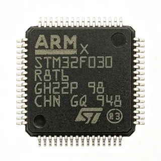
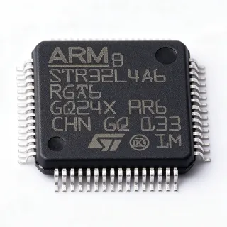
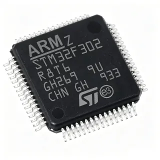
STM32F030R8T6TR - 64KB Flash ARM Cortex-M0 48MHz MCU | STMicroelectronics (Tape & Reel)
MPN: STM32F030R8T6TR ✓ 啟用中STM32F030R8T6TR 概覽
What is a microcontroller? A microcontroller (MCU) is a compact integrated circuit that combines a processor core, volatile and non-volatile memory, and programmable I/O peripherals on a single silicon die. The STM32F030R8T6TR belongs to the broader STM32 family of 32-bit ARM Cortex-M microcontrollers, with its Cortex-M0 core positioning it in the entry-level, low-power tier that targets cost-sensitive applications replacing 8-bit/16-bit legacy MCUs.
Key features include 64KB of Flash, 8KB of SRAM, an integrated 12-bit ADC with up to 16 channels, a 12-bit DAC, multiple 16-bit and 32-bit timers, two I2C, two SPI, and up to five USART interfaces, plus a hardware CRC calculation unit. The 64-pin LQFP package supports surface-mount assembly and provides generous analog and digital I/O for mixed-signal embedded boards.
Architecturally, the device uses a 32-bit ARM Cortex-M0 core with single-cycle I/O access, achieving 0.9 DMIPS/MHz and supporting Thumb-2 instruction subsets for compact code density. Built-in peripherals include a real-time clock (RTC), DMA controller, and power-on reset/power-down reset (POR/PDR), with multiple low-power modes to extend battery runtime. The integrated 8 MHz HSI oscillator is factory-trimmed to within 1 percent accuracy, reducing the bill of materials for cost-driven designs.
Typical applications include industrial control, consumer electronics, IoT edge nodes, home automation, motor control, and sensor interfaces. The wide peripheral set, small package, and low cost make it well suited to high-volume products where deterministic real-time response is required.
When designing with this MCU, provide decoupling capacitors on every VDD pin (100 nF ceramic + 4.7 uF bulk), use the SWD interface for in-system programming and on-chip debug, and verify that the external crystal load capacitance matches the oscillator specification when an HSE source is required.
This page synthesizes distributor pricing, drop-in package-compatible alternatives, and practical design notes beyond what the ST datasheet provides, delivering a consolidated reference for engineers evaluating the STM32F030R8T6TR.
直接替換替代品,適用於 STM32F030R8T6TR — 相同封裝,腳位對腳位相容。需重新設計 PCB 的不同封裝零件不列入。
此系列的變體
與下列產品可直接替換的同系列型號: STM32F030R8T6TR (相同外形與佔位) — 差異在於 Package, Timers, Core, Communication Interfaces, Flash Memory.
STM32F030C8T6
✅ 直接替換聯絡詢價
查看資料表 →STM32F051R8T6
✅ 直接替換聯絡詢價
查看資料表 →STM32F072RBT6
✅ 直接替換聯絡詢價
查看資料表 →GD32F130R8T6
✅ 直接替換📋 參考替代品(不在目錄中)
HK32F030R8T6
✅ 直接替換📋 參考替代品(不在目錄中)
STM32G030K8T6
✅ 直接替換聯絡詢價
查看資料表 →STM32F030R8T6TR 最大額定值與電氣特性
| Core Architecture | ARM Cortex-M0 (32-bit) |
| Series | STM32F0 Value Line |
| 最大時脈頻率 | 48 MHz |
| Program Memory (Flash) | 64 KB |
| SRAM | 8 KB |
| Supply Voltage Range | 2.4 V to 3.6 V |
| 工作溫度範圍 | -40 C to +85 C (industrial) |
| GPIO Pins | 51 |
| 封裝 | LQFP-64 (10x10 mm) |
| ADC | 1 x 12-bit, up to 16 channels |
| DAC | 1 x 12-bit |
| Communication Interfaces | 5x USART, 2x SPI, 2x I2C |
| Timers | 1 x 16-bit advanced, 5 x 16-bit general, 1 x 16-bit basic, 1 x 32-bit SysTick, 2 x watchdog |
| DMA Channels | 5 channels |
| On-chip Oscillator | 8 MHz HSI (factory-trimmed) |
| Debug Interface | Serial Wire Debug (SWD) |
| 安裝類型 | Surface Mount |
| RoHS 狀態 | Compliant |
STM32F030R8T6TR 腳位配置
| 腳位 1 | VBAT — Backup battery supply for RTC and backup registers |
| 腳位 2 | PC13 — GPIO port C bit 13; can be configured as Tamper, TimeStamp, or Wakeup |
| 腳位 3 | PC14 — GPIO port C bit 14; OSC32_IN or oscillator pin |
| 腳位 4 | PC15 — GPIO port C bit 15; OSC32_OUT or oscillator pin |
| 腳位 5 | OSC_IN — External clock input (HSE) or crystal connection |
| 腳位 6 | OSC_OUT — External clock output (HSE) or crystal connection |
| 腳位 7 | NRST — External reset input, active low |
| 腳位 8 | VSSA — Analog ground |
| 腳位 9 | VDDA — Analog supply voltage (2.4 V to 3.6 V) |
| 腳位 10 | PA0 — GPIO/ADC IN0/WKUP1/TIM2_CH1 |
| 腳位 11 | PA1 — GPIO/ADC IN1/TIM2_CH2 |
| 腳位 12 | PA2 — GPIO/USART1_TX/ADC IN2/TIM2_CH3 |
| 腳位 13 | PA3 — GPIO/USART1_RX/ADC IN3/TIM2_CH4 |
| 腳位 14 | PA4 — GPIO/SPI1_NSS/USART1_CK/ADC IN4/DAC_OUT1 |
| 腳位 15 | PA5 — GPIO/SPI1_SCK/ADC IN5/DAC_OUT2 |
| 腳位 16 | PA6 — GPIO/SPI1_MISO/ADC IN6 |
| 腳位 17 | PA7 — GPIO/SPI1_MOSI/ADC IN7 |
| 腳位 18 | PB0 — GPIO/ADC IN8/TIM3_CH3 |
| 腳位 19 | PB1 — GPIO/ADC IN9/TIM3_CH4 |
| 腳位 20 | PB2 — GPIO/BOOT1 |
| 腳位 21 | PB10 — GPIO/I2C2_SCL/USART3_TX |
| 腳位 22 | PB11 — GPIO/I2C2_SDA/USART3_RX |
| 腳位 23 | VSS_1 — Digital ground |
| 腳位 24 | VDD_1 — Digital supply voltage (2.4 V to 3.6 V) |
| 腳位 25 | PB12 — GPIO/SPI2_NSS/TIM1_BKIN |
| 腳位 26 | PB13 — GPIO/SPI2_SCK/TIM1_CH1N |
| 腳位 27 | PB14 — GPIO/SPI2_MISO/TIM1_CH2N |
| 腳位 28 | PB15 — GPIO/SPI2_MOSI/TIM1_CH3N |
| 腳位 29 | PA8 — GPIO/USART1_CK/TIM1_CH1 |
| 腳位 30 | PA9 — GPIO/USART1_TX/TIM1_CH2 |
| 腳位 31 | PA10 — GPIO/USART1_RX/TIM1_CH3 |
| 腳位 32 | PA11 — GPIO/USART1_CTS/SPI1_MISO |
| 腳位 33 | PA12 — GPIO/USART1_RTS/SPI1_MOSI |
| 腳位 34 | PA13 — SWDIO (Serial Wire Debug data) |
| 腳位 35 | VSS_2 — Digital ground |
| 腳位 36 | VDD_2 — Digital supply voltage (2.4 V to 3.6 V) |
| 腳位 37 | PA14 — SWCLK (Serial Wire Debug clock) |
| 腳位 38 | PA15 — GPIO/SPI1_NSS/TIM2_CH1_ETR |
| 腳位 39 | PB3 — GPIO/SPI1_SCK/TIM2_CH2 |
| 腳位 40 | PB4 — GPIO/SPI1_MISO/TIM3_CH1 |
| 腳位 41 | PB5 — GPIO/SPI1_MOSI/I2C1_SMBA/TIM3_CH2 |
| 腳位 42 | PB6 — GPIO/I2C1_SCL/USART1_TX/TIM3_CH3 |
| 腳位 43 | PB7 — GPIO/I2C1_SDA/USART1_RX/TIM3_CH4 |
| 腳位 44 | BOOT0 — Boot memory selection (Flash or System memory) |
| 腳位 45 | PB8 — GPIO/I2C1_SCL/TIM3_CH3 |
| 腳位 46 | PB9 — GPIO/I2C1_SDA/TIM3_CH4 |
| 腳位 47 | PC6 — GPIO/TIM3_CH1 |
| 腳位 48 | PC7 — GPIO/TIM3_CH2 |
| 腳位 49 | PC8 — GPIO/TIM3_CH3 |
| 腳位 50 | PC9 — GPIO/TIM3_CH4 |
| 腳位 51 | PA0_WKUP — Wakeup pin / shared with PA0 |
| 腳位 52 | VSS_3 — Digital ground |
| 腳位 53 | VDD_3 — Digital supply voltage (2.4 V to 3.6 V) |
| 腳位 54 | PA11 — GPIO / I2C or USART (alternate function) |
| 腳位 55 | PC10 — GPIO/USART3_TX |
| 腳位 56 | PC11 — GPIO/USART3_RX |
| 腳位 57 | PC12 — GPIO/USART3_CK |
| 腳位 58 | PD2 — GPIO/TIM3_ETR |
| 腳位 59 | PB13 — GPIO / SPI2 alternate |
| 腳位 60 | PB14 — GPIO / SPI2 alternate |
| 腳位 61 | PB15 — GPIO / SPI2 alternate |
| 腳位 62 | PC0 — GPIO/ADC IN10 |
| 腳位 63 | PC1 — GPIO/ADC IN11 |
| 腳位 64 | VSS_4 — Digital ground (thermal pad reference for LQFP package) |
典型應用
STM32F030R8T6TR 適用於 7 應用s: Industrial Sensor Control, Home Automation Hubs, Consumer Remote Controls, Lighting LED Drivers, Motor Control (Small BLDC/PMSM), Medical Wearables and Devices, Automotive Body Electronics (Non-Safety).
Industrial Sensor Control
The STM32F030R8T6TR fits sensor hubs that aggregate 4-20 mA loops, digital temperature probes, and switches into a single low-cost node. The Cortex-M0 core running at 48 MHz provides 38 MHz of headroom for periodic polling plus interrupt-driven edge events, while the 12-bit ADC with up to 16 channels handles multiple analog sensors simultaneously. Engineers commonly pair the MCU with I2C-based digital sensors and output a clean USART telemetry stream at 115200 baud to a gateway PLC.
推薦
Home Automation Hubs
In Zigbee / Matter / Wi-Fi bridges or smart thermostats the STM32F030R8T6TR provides the user-interface MCU: it scans buttons, drives an LCD or OLED display, controls a buzzer, and exposes an I2C port to a wireless module. Its 2.4-3.6 V supply matches battery or USB-powered rails, and the RTC plus low-power Stop/Sleep modes extend coin-cell runtime. The 64 KB Flash accommodates Zigbee and BLE stack lite profiles along with vendor-specific application logic.
推薦
Consumer Remote Controls
Universal IR/RF remotes lean on the STM32F030R8T6TR because the 48 MHz core easily handles NEC, RC5, and SIRC protocols alongside BLE pairing. The 64 KB Flash stores the entire protocol library plus button layouts, while the 8 KB SRAM is sufficient for two-way RF acknowledgement buffers. The 51 GPIO pins and 5 USART instances allow expansion for scroll wheels, capacitive touch, and battery monitoring on a single chip.
推薦
Lighting LED Drivers
The STM32F030R8T6TR controls constant-current LED drivers for commercial luminaires via PWM-dimmable DC-DC converters and DMX-512/digital addressable lighting interfaces. Its five 16-bit timers generate PWM at frequencies well above the audible band (>20 kHz) to avoid coil whine, and the 16-bit advanced timer supports motor-control-style complementary PWM with dead-time insertion. The 12-bit DAC controls analog LED current sinks or analog dimming inputs.
推薦
Motor Control (Small BLDC/PMSM)
For low-voltage BLDC/PMSM motors below 100 W, the STM32F030R8T6TR runs sensorless field-oriented control (FOC) at 48 MHz with the help of its 16-bit advanced timer generating the six-step complementary PWM. The 12-bit ADC samples phase currents and BEMF at 50 kHz, satisfying rotor-position feedback. Its small LQFP-64 footprint keeps the power-stage PCB compact, and the wide -40 to +85 C range supports industrial deployments.
推薦
Medical Wearables and Devices
Low-risk medical wearables such as pedometers, pill dispensers, and pulse oximeter sub-boards use the STM32F030R8T6TR for sensor reading, simple TFT driving, and BLE notification duties. The 12-bit ADC accurately captures PPG/heart-rate analog signals, while the low-power Run, Sleep, and Stop modes extend battery life to weeks between charges. RoHS-compliant lead-free packaging and IEC 61000-4-2-friendly ESD pins ensure robustness for portable medical electronics.
推薦
Automotive Body Electronics (Non-Safety)
Body-control modules for non-safety functions (window lifts, mirror adjusters, ambient lighting) use the STM32F030R8T6TR when the application stays below AEC-Q100 requirements. Its -40 to +85 C grade handles under-dash thermal load, the 64 KB Flash fits LIN slave firmware plus diagnostic stacks, and the 5 USARTs expose dual LIN transceivers for body networks. The 12-bit ADC reads current sensing for stall detection on window motors, while timers drive MOSFET gate drivers.
推薦
推薦產品摘要
工程參考資料,適用於 STM32F030R8T6TR — 比較、設計指引及合規資訊。
選型指南
與替代品比較
| 參數 | 本產品 | STM32F030C8T6 | STM32F051R8T6 | STM32F072RBT6 | GD32F130R8T6 | HK32F030R8T6 | STM32G030K8T6 |
|---|---|---|---|---|---|---|---|
| Brand | STMicroelectronics | STMicroelectronics | STMicroelectronics | STMicroelectronics | GigaDevice | GigaDevice (second source) | STMicroelectronics |
| Package | LQFP-64 (10x10 mm) | LQFP-48 (7x7 mm) - not pin-compatible | LQFP-64 (10x10 mm) - same | LQFP-64 (10x10 mm) - same | LQFP-64 (10x10 mm) - same | LQFP-64 (10x10 mm) - same | LQFP-32 (7x7 mm) - not pin-compatible |
| Core | ARM Cortex-M0 32-bit | ARM Cortex-M0 | ARM Cortex-M0 | ARM Cortex-M0 | ARM Cortex-M3 | ARM Cortex-M0 | ARM Cortex-M0+ |
| Max Clock Frequency | 48 MHz | 48 MHz | 48 MHz | 48 MHz | 48 MHz | 48 MHz | 64 MHz |
| Flash Memory | 64 KB | 64 KB | 64 KB | 128 KB | 64 KB | 64 KB | 64 KB |
| SRAM | 8 KB | 8 KB | 8 KB | 16 KB | 8 KB | 8 KB | 8 KB |
| Supply Voltage | 2.4 V to 3.6 V | 2.4 V to 3.6 V | 2.0 V to 3.6 V | 2.0 V to 3.6 V | 2.6 V to 3.6 V | 2.4 V to 3.6 V | 2.0 V to 3.6 V |
| USB | No | No | Yes | Yes | No | No | No |
主要差異化特點
- Lowest-cost LQFP-64 part in the STM32F0 line with 64 KB Flash (對比STM32F072RBT6)
- Large LQFP-64 pin count gives 51 GPIO for fan-out expansion (對比STM32F030C8T6)
- Drops to a 48 MHz Cortex-M0 vs the GigaDevice M3 at the same price (對比GD32F130R8T6)
設計說明
Decouple every VDD pin with a 100 nF ceramic capacitor placed as close as possible to the package pin, and add a 4.7 uF bulk capacitor on each power domain (VDD_1, VDD_2, VDD_3, VDDA). The VDDA analog supply should be tied to a separate ferrite-bead-isolated rail for clean ADC sampling. Implement a power-on reset delay of at least 1 ms by using the internal POR rather than relying on an external RC.
Route the SWD signals (SWDIO, SWCLK, NRST) close together with a maximum 15 mm trace length to avoid debugger comm errors. Keep the HSE crystal and its load capacitors within 5 mm of the OSC_IN/OSC_OUT pins, with a ground guard ring around the oscillator area. Avoid routing any high-speed or switching signals across or under the analog ground (VSSA) island.
Do not enable the window watchdog (WWDG) during early firmware bring-up; it can lock up the MCU during breakpoints. Use the independent watchdog (IWDG) only after the application is stable, with reload value long enough to survive interrupt latency bursts. When entering Stop mode, ensure the HSI is selected before configuring external interrupts, otherwise the wake-up can cause a hard-fault on PLL startup.
合規資訊
RoHS and REACH compliance per ST product page; LQFP-64 package with lead-free matte-tin plating. Industrial temperature grade is -40 C to +85 C; for AEC-Q100, step up to AEC-Q100 qualified STM32 parts such as SPC58 or STM32G0 automotive variants.