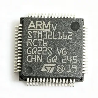
STM32F051R8T6 - 48MHz Cortex-M0 MCU, 64KB Flash | ST
MPN: STM32F051R8T6 ✓ Active| Qty | Unit Price | Extended |
|---|---|---|
| 1 | $3.85 | $3.85 |
| 10 | $3.45 | $34.50 |
| 100 | $3.05 | $305.00 |
| 500 | $2.75 | $1,375.00 |
| 1,000 | $2.45 | $2,450.00 |
STM32F051R8T6 Overview
A microcontroller (MCU) integrates a processor core, non-volatile memory, SRAM, and a rich set of peripherals onto a single silicon die, forming the lowest tier of the computing hierarchy: transistor -> logic gate -> processor core -> microcontroller -> embedded system. Within STMicroelectronics' portfolio, the STM32F0 entry-level series sits below the mainstream STM32F1/F4 families and provides Cortex-M0 cost efficiency while retaining STM32 tooling, peripheral architecture, and software ecosystem compatibility.
Key features of the STM32F051R8T6 include 11 timers covering basic, general-purpose, and advanced (motor-control) functions, a 12-bit 1 Msps ADC, a 12-bit DAC, up to 55 GPIO lines, and communication interfaces spanning USART, SPI, I2C, and CEC. A CRC calculation unit, programmable watchdogs, and POR/PDR reset circuitry improve design robustness. Supply voltage spans 2.0V to 3.6V, simplifying integration into battery- and USB-adjacent designs.
Technically, the Cortex-M0 core executes Thumb instruction subset code with a 32-bit datapath and a nested vectored interrupt controller (NVIC) delivering deterministic low-latency interrupts. The embedded Flash supports in-system programming via USART, while the flexible clock tree accepts an internal 8 MHz HSI or external crystal sources up to 48 MHz system frequency.
Typical applications include industrial automation sensors and actuators, consumer appliances, motor control with the advanced timers, IoT sensor nodes, and system auxiliary control functions.
Designers should budget SRAM carefully: 8 KB is ample for bare-metal control loops but limits large buffers or complex stacks; enable hardware CRC and DMA offload to free CPU cycles.
This page adds value beyond the manufacturer datasheet by consolidating verified distributor specifications, drop-in alternatives, cross-brand substitution guidance, and practical design notes for the STM32F051R8T6.
Drop-in alternatives for STM32F051R8T6 — same package, pin-to-pin compatible. Different-package parts requiring PCB rework are excluded.
Quick Comparison Tool — Select alternative parts for side-by-side comparison:
STM32F051R8T7
✅ Drop-In📋 Reference alternative (not in catalog)
STM32F051R6T6
✅ Drop-In ⚠️ 参数待验证📋 Reference alternative (not in catalog)
STM32F042R6T6
✅ Drop-In ⚠️ 参数待验证📋 Reference alternative (not in catalog)
STM32F031R6T6
✅ Drop-In ⚠️ 参数待验证📋 Reference alternative (not in catalog)
GD32F130R8T6
✅ Drop-In📋 Reference alternative (not in catalog)
STM32F051R8T6 Maximum Ratings & Electrical Characteristics
| Core | ARM Cortex-M0, 32-bit |
| Maximum CPU Frequency | 48 MHz |
| Flash Memory | 64 KB |
| SRAM | 8 KB |
| Supply Voltage Range | 2.0 V to 3.6 V |
| GPIO Count | 55 I/O |
| Timers | 11 (basic, general-purpose, advanced) |
| ADC | 12-bit, 1 Msps |
| DAC | 12-bit |
| Communication Interfaces | USART, SPI, I2C, CEC |
| CRC Unit | Yes |
| Reset | POR/PDR (power-on / power-down reset) |
| Oscillator Type | Internal (HSI) and external |
| Package | LQFP-64 |
| Mounting Type | Surface Mount |
| Program Memory Type | FLASH |
| RoHS Status | Compliant |
STM32F051R8T6 Pin Configuration
| Pin 1 | VBAT — Backup battery supply for RTC |
| Pin 2 | PC13 — GPIO / RTC functions |
| Pin 3 | PC14-OSC32_IN — GPIO / 32.768 kHz oscillator input |
| Pin 4 | PC15-OSC32_OUT — GPIO / 32.768 kHz oscillator output |
| Pin 5 | PH0-OSC_IN — Main oscillator input |
| Pin 6 | PH1-OSC_OUT — Main oscillator output |
| Pin 7 | NRST — System reset (active low) |
| Pin 8 | PC0 — GPIO / ADC input |
| Pin 9 | PC1 — GPIO / ADC input |
| Pin 10 | PC2 — GPIO / ADC input |
| Pin 11 | PC3 — GPIO / ADC input |
| Pin 12 | VSSA — Analog ground |
| Pin 13 | VDDA — Analog supply |
| Pin 14 | PA0 — GPIO / ADC / wake-up |
| Pin 15 | PA1 — GPIO / ADC |
| Pin 16 | PA2 — GPIO / USART2_TX / ADC |
| Pin 17 | PA3 — GPIO / USART2_RX / ADC |
| Pin 18 | PA4 — GPIO / SPI1_NSS / DAC_OUT1 |
| Pin 19 | PA5 — GPIO / SPI1_SCK / DAC_OUT2 |
| Pin 20 | PA6 — GPIO / SPI1_MISO / ADC |
| Pin 21 | PA7 — GPIO / SPI1_MOSI / ADC |
| Pin 22 | PC4 — GPIO / ADC input |
| Pin 23 | PC5 — GPIO / ADC input |
| Pin 24 | PB0 — GPIO / ADC input |
| Pin 25 | PB1 — GPIO / ADC input |
| Pin 26 | PB2 — GPIO / BOOT1 |
| Pin 27 | PB10 — GPIO / I2C2_SCL / USART3_TX |
| Pin 28 | PB11 — GPIO / I2C2_SDA / USART3_RX |
| Pin 29 | VSS_1 — Ground |
| Pin 30 | VDD_1 — Digital supply |
| Pin 31 | PB12 — GPIO / SPI2_NSS |
| Pin 32 | PB13 — GPIO / SPI2_SCK |
| Pin 33 | PB14 — GPIO / SPI2_MISO |
| Pin 34 | PB15 — GPIO / SPI2_MOSI |
| Pin 35 | PC6 — GPIO |
| Pin 36 | PC7 — GPIO |
| Pin 37 | PC8 — GPIO |
| Pin 38 | PC9 — GPIO |
| Pin 39 | PA8 — GPIO / USART1_CK / MCO |
| Pin 40 | PA9 — GPIO / USART1_TX |
| Pin 41 | PA10 — GPIO / USART1_RX |
| Pin 42 | PA11 — GPIO / CEC / TIM1_CH4 |
| Pin 43 | PA12 — GPIO / CEC |
| Pin 44 | PA13 — GPIO / SWDIO (debug) |
| Pin 45 | VSS_2 — Ground |
| Pin 46 | VDD_2 — Digital supply |
| Pin 47 | PA14 — GPIO / SWCLK (debug) |
| Pin 48 | PA15 — GPIO / SPI1_NSS |
| Pin 49 | PC10 — GPIO / USART3_TX |
| Pin 50 | PC11 — GPIO / USART3_RX |
| Pin 51 | PC12 — GPIO / USART3_CK |
| Pin 52 | PD2 — GPIO / USART3_RX |
| Pin 53 | PB3 — GPIO / SPI1_SCK / SWO |
| Pin 54 | PB4 — GPIO / SPI1_MISO |
| Pin 55 | PB5 — GPIO / SPI1_MOSI / I2C1_SMBA |
| Pin 56 | PB6 — GPIO / I2C1_SCL / USART1_TX |
| Pin 57 | PB7 — GPIO / I2C1_SDA / USART1_RX |
| Pin 58 | BOOT0 — Boot mode selection |
| Pin 59 | PB8 — GPIO / I2C1_SCL / CEC |
| Pin 60 | PB9 — GPIO / I2C1_SDA |
| Pin 61 | VSS_3 — Ground |
| Pin 62 | VDD_3 — Digital supply |
| Pin 63 | PB8/PB9-BOOT — GPIO / boot pin alternate bonding |
| Pin 64 | VDDIO2 — I/O supply domain 2 |
Typical Applications
STM32F051R8T6 is suitable for 6 applications: Industrial Automation Sensors and Actuators, Low-Voltage Motor Control, IoT Sensor Nodes, Consumer Appliances and White Goods, USB-Adjacent and CEC Consumer Electronics, System Management and Auxiliary Control.
Industrial Automation Sensors and Actuators
The STM32F051R8T6 fits industrial sensing and actuation nodes because its 12-bit 1 Msps ADC digitizes analog sensor channels with adequate resolution, and 55 GPIO plus USART/SPI/I2C interfaces integrate encoders, displays, and field-bus bridges. The 2.0V-3.6V tolerant supply with POR/PDR reset gives robust power-up behavior in noisy factory environments. In typical use the MCU runs a bare-metal control loop reading sensor data via DMA-driven ADC conversions, applying filtering, and driving relays or actuators through general-purpose timers. The hardware CRC unit validates communication frames without CPU overhead. The constraint to plan for is 8 KB SRAM - keep buffering shallow and avoid large protocol stacks.
Recommended
Low-Voltage Motor Control
For BLDC/DC fan and pump motor control, the STM32F051R8T6 offers advanced-control timers with complementary PWM outputs and dead-time insertion - precisely the features a three-phase inverter bridge needs. The synchronized 12-bit ADC samples phase current shunts mid-PWM-cycle, supporting sensorless back-EMF commutation or hall-sensored control on the 48 MHz Cortex-M0 core. ST application examples target exactly this configuration within the STM32F0 ecosystem. Designers must respect the 8 KB SRAM budget when implementing observers, and should verify ADC injection-sampling timing in the reference manual before finalizing firmware, since peripheral density is moderate on this entry-level device.
Recommended
IoT Sensor Nodes
Battery-adjacent IoT nodes benefit from the STM32F051R8T6's 2.0V operation - the MCU keeps running as a battery discharges - while low run power and multiple low-power modes extend field life. On-chip SPI/I2C interfaces connect RF modules and MEMS sensors, and the 12-bit ADC monitors battery voltage and analog probes. A typical topology pairs the MCU with a sub-GHz or BLE radio module over UART, waking on sensor threshold interrupts via EXTI lines. The key trade-off is the absence of larger SRAM for TLS stacks, so designs needing heavy cryptography should either externalize connectivity intelligence to the module or select a higher-memory pin-compatible STM32.
Recommended
Consumer Appliances and White Goods
The STM32F051R8T6 suits appliance control boards: 55 GPIO drive keypads, indicators, and relays, while 11 timers manage touch-sensing, buzzer tones, PWM loads, and watchdog supervision. The on-chip CEC interface supports HDMI-CEC control paths in AV appliances. Its 3.3V operation and internal oscillator remove the cost of external crystals in non-timing-critical products, and the CRC unit plus POR/PDR improve resilience against mains-borne transients. Compliance-oriented appliance designs commonly pair this MCU with isolated AC-line sensing. Firmware is developed in STM32CubeIDE using the standard peripheral model, keeping certification rework low when migrating within the STM32F0 family.
Recommended
USB-Adjacent and CEC Consumer Electronics
With a 2.0V-3.6V supply and CEC support, the STM32F051R8T6 integrates into consumer electronics subsystems that need a co-processor for button decoding, IR/CEC protocol handling, and power sequencing under main-SoC control. USART and I2C links to the host are straightforward, and the 64 KB Flash accommodates protocol stacks plus OTA-style firmware field updates implemented as user bootloaders. Note that this exact part lacks a native USB controller; for designs that must enumerate USB directly, the pin-compatible STM32F042R6T6 alternative adds a USB device peripheral while retaining the LQFP-64 footprint, making the migration a low-risk drop-in.
Recommended
System Management and Auxiliary Control
As a system-management co-processor, the STM32F051R8T6 supervises fans, power rails, and front panels in networking and instrumentation equipment. Its 12-bit ADC reads thermistors and rail voltages, PWM timers drive fan channels, and USART links report telemetry to a host CPU or FPGA board. The deterministic Cortex-M0 NVIC keeps monitoring loops responsive even under interrupt storms, and watchdog timers guarantee recovery from host crashes. When used alongside XAIPART FPGA products such as the Intel/Altera MAX 10 family, the MCU handles slow housekeeping while the FPGA manages high-speed logic - a proven architecture for cost-optimized embedded platforms.
Recommended
Recommended Products Summary
Engineering reference data for STM32F051R8T6 — comparison, design guidance, and compliance information.
Selection Guide
Comparison with Alternatives
| Parameter | This Product | STM32F051R8T7 | STM32F051R6T6 | STM32F042R6T6 | GD32F130R8T6 |
|---|---|---|---|---|---|
| Package | LQFP-64 | LQFP-64 - same | LQFP-64 - same | LQFP-64 - same | LQFP-64 - same |
| Brand | STMicroelectronics | STMicroelectronics | STMicroelectronics | STMicroelectronics | GigaDevice |
| Core / Max Frequency | ARM Cortex-M0, 48 MHz | Cortex-M0, 48 MHz | Cortex-M0, 48 MHz | Cortex-M0, 48 MHz | Cortex-M0, up to 72 MHz |
| Flash Memory | 64 KB | 64 KB | 32 KB | 32 KB | 64 KB |
| Supply Voltage | 2.0 V - 3.6 V | 2.0 V - 3.6 V | 2.0 V - 3.6 V | 2.0 V - 3.6 V | 2.6 V - 3.6 V |
Key Differentiators
- Full 64 KB Flash within the pin-compatible family (vs STM32F051R6T6)
- Guaranteed ST datasheet compatibility (vs GD32F130R8T6)
- Advanced timers with complementary PWM and dead-time (vs STM32F031R6T6)
- Trade-off: no native USB controller (vs STM32F042R6T6)
Design Notes
Decouple each VDD pin (pins 30, 46, 62/64 domain) with a 100 nF ceramic capacitor placed within 3 mm of the pin, plus one 4.7 uF bulk capacitor near the regulator output. The VDDA/VSSA pair (pins 13/12) requires a separate ferrite bead and 1 uF + 10 nF filtering to preserve the 12-bit ADC's effective resolution; injecting switching-regulator ripple into VDDA is the most common cause of ADC noise complaints on STM32F0 boards.
The LQFP-64 thermal pad is absent, so heat exits through the leads - normal for the sub-100 mW dissipation of this MCU. Instead, prioritize trace fan-out: route the SWDIO (pin 44) and SWCLK (pin 47) debug lines to a 4-pin header before final layout, because rework to access them later is difficult. Keep BOOT0 (pin 58) tied through a 10 kOhm pulldown to GND with a test point for firmware recovery via the built-in USART bootloader.
Do not assume flash wait-state timing identical across the family: when cross-brand substituting with GigaDevice GD32F130R8T6, flash zero-wait-state behavior differs and tight timing loops calibrated on the STM32F051R8T6 at 48 MHz will shift. Also confirm the operating temperature requirement before choosing T6 over the T7 industrial grade - consumer grade T6 parts are not specified for extended industrial ambients, and field failures in sealed enclosures often trace to this suffix-level mismatch.
Estimated: with a 48 MHz core clock the GPIO edges are fast enough (typically low-ns class) to generate noticeable ringing on un-terminated ribbon-cable loads; add 22-33 Ohm series resistors on lines leaving the board and on USART TX/RX to external modules. This simple practice, taken from ST EME (electromagnetic compatibility) application guidance for STM32 families, reduces radiated emissions at low development cost.
Compliance Information
RoHS compliance per STMicroelectronics standard product listing for STM32F0 series. REACH, halogen-free, and conflict-minerals status not stated in provided web data - verify on st.com product compliance portal.