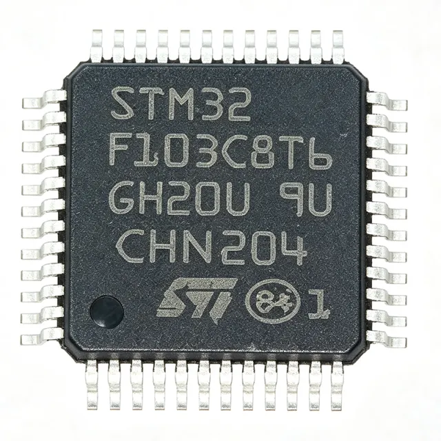
STM32F103C8T6
The STM32F103C8T6 is an active STMicroelectronics 32-bit microcontroller built around the Arm Cortex-M3 core. According to the STMicroelectronics product page, the STM32F103xx medium-density performance-line family operates at up to 72 MHz. The device provides 64 KB of Flash, 20 KB of SRAM, two 12-bit ADCs, seven 16-bit timers, and interfaces including USART, SPI, I2C, USB, and CAN in an LQFP-48 package.
What are the key specifications of STM32F103C8T6 that engineers should know?
The STM32F103C8T6 combines a 72 MHz Arm Cortex-M3 core with 64 KB of Flash and 20 KB of SRAM. Its integrated peripherals include two 12-bit ADCs, seven 16-bit timers, and USART, SPI, I2C, USB, and CAN communication interfaces. The manufacturer identifies the device as an active member of the STM32F103xx medium-density performance line and packages it in LQFP-48 for surface-mounted PCB assembly.
Where to download the STM32F103C8T6 datasheet PDF?
The official STM32F103C8T6 datasheet PDF is available from STMicroelectronics at https://www.st.com/resource/en/datasheet/stm32f103c8.pdf. The datasheet contains the device description, electrical characteristics, memory map, peripheral information, package information, and pin definitions. Use the manufacturer document for final schematic, decoupling, clock, and operating-limit decisions rather than relying on a third-party copy.
Where can I find the STM32F103C8T6 pinout?
The STM32F103C8T6 pinout is documented in the pin-description section of the official STMicroelectronics STM32F103C8 datasheet. The component uses a 48-pin LQFP package and exposes 37 I/O ports together with power, ground, reset, clock, boot, and programming signals. Assign every PCB trace from the package drawing and pin table because several alternate-function mappings depend on the peripheral configuration.
What is the STM32F103C8T6 blue pill and what should its pinout include?
The STM32F103C8T6 blue pill is a widely used development board built around the STM32F103C8T6 rather than a different MCU package. Its board-level header exposes only a selected subset of the LQFP-48 device signals, so the board schematic is necessary to trace each header pin. Engineers should still use the manufacturer’s LQFP-48 pin table when designing a production PCB.
What does STM32F103C8T6 schematic need for power, reset, and clock?
A practical STM32F103C8T6 schematic must support the stated 2.0 V to 3.6 V operating range, normally using a 3.3 V rail, and must include the manufacturer-recommended input and output decoupling. Reset, boot configuration, clock sourcing, and programming-debug connections must follow the datasheet and reference design. Verify startup behavior and SWD connectivity on the final layout before releasing a multi-board production run.
Where to buy STM32F103C8T6 online?
The STM32F103C8T6 can be requested through the Request a Quote form on this page. The form is the appropriate channel for checking current availability, order quantities, delivery timing, and shipment options. Because MCU inventory and lead times can change by lot and market conditions, request a quote for the exact LQFP-48 ordering code rather than relying on a historical stock count.
What is the price of STM32F103C8T6?
Current STM32F103C8T6 commercial terms should be obtained through the Request a Quote form on this page. Pricing can depend on quantity, date code, traceability requirements, packaging format, and market inventory, so a historical amount would not reliably represent current availability. Submit the required quantity and shipment destination to receive the applicable quotation directly.
What is the lead time for STM32F103C8T6?
The current STM32F103C8T6 lead time should be confirmed through the Request a Quote form on this page. Lead time can vary with factory inventory, planned production, and the requested quantity. Include the required delivery date and any component-approval constraints in the request so the supply plan can be based on the same device ordering code and package.
Is STM32F103C8T6 in stock?
STM32F103C8T6 availability is best checked through the Request a Quote form on this page. The manufacturer lists the STM32F103C8 family as active, but that lifecycle statement does not guarantee immediate stock for every package suffix and quantity. Submit the exact MPN, target quantity, and required date to obtain the current supply response.
STM32F103C8T6 vs STM32F103CBT6: which is better for an LQFP-48 design?
STM32F103CBT6 is the closest same-family alternative identified for an LQFP-48 design, while STM32F103C8T6 remains the defined 64 KB Flash and 20 KB SRAM configuration. The C8T6 is the better selection when firmware is already qualified specifically against that memory profile. Confirm the C-series pin assignments, Flash organization, and device identifier in the manufacturer documentation before treating the parts as interchangeable.
What is the difference between STM32F103C8T6 and GD32F103C8T6?
GD32F103C8T6 is identified as a pin-compatible alternative with the same Cortex-M3 core, 64 KB Flash, 20 KB SRAM, and LQFP-48 package, but it is rated up to 108 MHz rather than 72 MHz. That 50% clock increase can affect wait states and timing. Treat it as an engineering-review second source rather than assuming unchanged firmware or identical electrical behavior.
When should I choose STM32F103C8T6 over GD32F103C8T6?
Choose STM32F103C8T6 when the design has an established STMicroelectronics firmware baseline, existing tooling, or approved peripheral behavior at 72 MHz. Choose GD32F103C8T6 only after reviewing clock configuration, flash wait states, startup code, interrupt behavior, USB, CAN, and toolchain compatibility. Its 108 MHz maximum clock is 50% higher, so clock-sensitive software must be deliberately qualified.
Is STM32F103C8T6 suitable for industrial control and motor-drive designs?
The STM32F103C8T6 is suitable for many industrial control, motor-drive, and embedded-measurement designs because it combines a 72 MHz Cortex-M3 core, two 12-bit ADCs, seven 16-bit timers, and multiple serial interfaces. It also supports CAN, which is useful for networked industrial nodes. Suitability still depends on motor-drive topology, isolation, protection, timing margins, environmental qualification, and the selected package’s thermal performance.
What can replace STM32F103C8T6?
GD32F103C8T6, APM32F103C8T6, CH32F103C8T6, and MM32F103C8T6 are identified as Cortex-M3 alternatives with the same headline 64 KB Flash, 20 KB SRAM, and LQFP-48 configuration. Their implementations still require board-level and firmware validation. The GD32F103C8T6 runs to 108 MHz versus 72 MHz, while the other alternatives require review of USB, CAN, startup, peripheral, and ecosystem differences.
Is STM32F103C8T6 the same as APM32F103C8T6?
STM32F103C8T6 and APM32F103C8T6 share the headline combination of an Arm Cortex-M3 core, 64 KB Flash, 20 KB SRAM, and LQFP-48 package. They are not automatically identical in every peripheral, clock, startup, or firmware detail. A substitution should proceed through schematic comparison, register and interrupt checks, timing tests, USB or CAN tests where applicable, and a production firmware regression.
What is the best GigaDevice equivalent for STM32F103C8T6?
GD32F103C8T6 is the best-supported GigaDevice alternative identified for STM32F103C8T6 because it matches the Cortex-M3 architecture, 64 KB Flash, 20 KB SRAM, and LQFP-48 package. Its maximum clock is 108 MHz, which is 50% above the STM32F103C8T6 limit. Validate clock timing, flash wait states, peripheral behavior, startup, and debug tooling before production use.