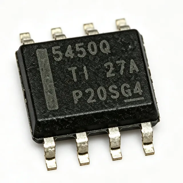
TPS5450QDDARQ1 - 5A 36V Automotive Buck Converter | TI
MPN: TPS5450QDDARQ1 ✓ 啟用中| 數量 | 單價 | 小計 |
|---|---|---|
| 1 | $2.63 | $2.63 |
| 10 | $2.4 | $24.00 |
| 100 | $2.15 | $215.00 |
| 500 | $1.95 | $975.00 |
| 1,000 | $1.8 | $1,800.00 |
TPS5450QDDARQ1 概覽
A DC-DC buck converter is a switching voltage regulator that steps a higher input voltage down to a lower regulated output using PWM switching, achieving far higher efficiency than linear regulators. Within the power management IC hierarchy, the TPS5450-Q1 is a non-synchronous, internally compensated voltage-mode SWIFT converter IC.
Key features include a 500 kHz fixed switching frequency, voltage-mode PWM control, an active-high enable (ENA) pin that reduces shutdown supply current to 18 uA, and full protection: cycle-by-cycle overcurrent limiting, overvoltage protection, and thermal shutdown. Internal feedback-loop compensation dramatically reduces external component count and design complexity.
Technically, the integrated high-side N-channel MOSFET and internal compensation allow a minimal external BOM - only an inductor, catch diode, feedback divider, and small input/output capacitors. The PowerPAD (DDA) package provides a low thermal impedance path to the PCB, and the 500 kHz switching frequency permits a compact inductor while keeping switching losses manageable across the 36V automotive input range, including load-dump-tolerant designs.
Typical applications include automotive infotainment and cluster 5V rails, ADAS and body-control module 12V-to-5V point-of-load conversion, and industrial 24V-bus step-down supplies where wide input headroom and 5A capability are required.
Design consideration: because the converter is non-synchronous, select a Schottky catch diode rated for the full output current with low forward drop, placed close to the PH pin; the exposed PowerPAD must be soldered to a solid ground copper pour for thermal performance.
This page synthesizes distributor pricing, same-brand drop-in alternatives, and practical design notes not found in the manufacturer datasheet, with prices as of 2026-09-01.
直接替換替代品,適用於 TPS5450QDDARQ1 — 相同封裝,腳位對腳位相容。需重新設計 PCB 的不同封裝零件不列入。
此系列的變體
與下列產品可直接替換的同系列型號: TPS5450QDDARQ1 (相同外形與佔位) — 差異在於 Maximum Output Current, Output Voltage Range, Package, Input Voltage Range, Operating Temperature.
快速比較工具 — 選擇替代零件進行並排比較:
TPS5450DDAR
✅ 直接替換聯絡詢價
查看資料表 →TPS5450DDARG4
✅ 直接替換📋 參考替代品(不在目錄中)
TPS5450MDDAREP
✅ 直接替換📋 參考替代品(不在目錄中)
TPS54360QDDARQ1
✅ 直接替換✗ 缺貨
$2.45 / 單位
查看資料表 →TPS54560BDDA
✅ 直接替換📋 參考替代品(不在目錄中)
TPS5450QDDARQ1 最大額定值與電氣特性
| 拓撲 | Step-Down (Buck), Non-Synchronous |
| 輸入電壓範圍 | 5.5 V to 36 V |
| 輸出電壓範圍 | 1.221 V to 31 V |
| 最大輸出電流 | 5 A continuous (6 A peak) |
| 輸出數量 | 1 |
| 切換頻率 | 500 kHz |
| Control Method | Voltage Mode PWM, Internally Compensated |
| 同步整流器 | No |
| Shutdown Supply Current | 18 uA (typ, via ENA pin) |
| 致能腳位 | Yes (active-high ENA) |
| Protections | Overcurrent limiting, OVP, thermal shutdown |
| 工作溫度 | -40 C to +125 C |
| 封裝 | HSOIC (DDA) 8-PowerSOIC, 3.90 mm width, PowerPAD |
| 安裝類型 | Surface Mount |
| Automotive Qualification | AEC-Q100 Qualified, PPAP supported |
| ECCN (US) | EAR99 |
| HTS | 8542.39.00.90 |
| RoHS 狀態 | Compliant |
TPS5450QDDARQ1 hsoic (dda) 8-powersoic, 3.90 mm width, powerpad 腳位配置指南
TPS5450QDDARQ1(hsoic (dda) 8-powersoic, 3.90 mm width, powerpad 封裝)的腳位配置。 此功率元件具有閘極、汲極與源極端子。對於非極性封裝,請參閱製造商資料表以取得確切的第 1 腳方向與佈局詳細資訊。常見應用包括電源設計、馬達驅動與負載切換。

無詳細腳位定義資料: TPS5450QDDARQ1.
請參閱 資料表 以查看完整腳位配置。
典型應用
TPS5450QDDARQ1 適用於 6 應用s: Automotive Infotainment 5V Rails, ADAS and Body Control Module Point-of-Load, Industrial 24V Bus Step-Down, USB Charging and Display Bias Rails, Battery-Powered Test and Measurement Instruments, Communications and Networking Equipment.
Automotive Infotainment 5V Rails
The TPS5450QDDARQ1 fits automotive infotainment and instrument-cluster 5V rails because its 5.5V to 36V input range covers cold-crank and load-dump-protected battery conditions, while the 5A continuous output powers SoCs, displays, and audio amplifiers from a single IC. The AEC-Q100 qualification and -40C to +125C operation satisfy automotive environment requirements. Placed as the first stage after the battery-protection block at a 500 kHz switching frequency, it allows a compact inductor; the PowerPAD DDA package solders to a ground copper pour that dissipates conduction and switching losses without a heatsink, keeping the module profile low.
推薦
ADAS and Body Control Module Point-of-Load
ADAS sensors, radar supplies, and body-control modules need dense 12V-to-5V or 12V-to-3.3V conversion with wide input tolerance. The TPS5450QDDARQ1's internally compensated voltage-mode control minimizes external parts, and its 1.221V reference supports low-voltage logic rails via a resistor divider. Cycle-by-cycle overcurrent limiting, overvoltage protection, and thermal shutdown provide the fault robustness that ASIL-oriented architectures expect. The 18 uA ENA-pin shutdown current permits always-connected modules to meet key-off quiescent budgets, and the 500 kHz fixed frequency keeps switching noise out of sensitive analog and RF sensor bands when the layout follows TI's PowerPAD reference design.
推薦
Industrial 24V Bus Step-Down
Factory automation and PLC systems run from 24V buses with significant tolerance, and the TPS5450QDDARQ1's 36V maximum input absorbs common transients while delivering 5A to motors' logic stages, IO modules, and embedded controllers. Although this part carries automotive qualification, its wide input, robust protection set, and DDA PowerPAD thermal design make it equally effective in industrial power trees. A Schottky catch diode rated above 5A peak placed at the PH pin, plus a shielded compact inductor selected for 500 kHz ripple current, yields a high-efficiency point-of-load stage; the exposed pad soldered to a ground plane manages the dissipation in enclosed DIN-rail housings.
推薦
USB Charging and Display Bias Rails
USB charging ports and display backplane bias rails require regulated 5V to 12V outputs at several amps, and the TPS5450QDDARQ1 covers both directions of this range with its adjustable 1.221V to 31V output. Its 5A continuous rating supports dual-port USB charging, and the active-high ENA pin allows a host controller to gate the rail for power sequencing or load management, dropping to 18 uA when off. The 500 kHz switching frequency places ripple above audio and AM radio bands with modest filtering, and the internal compensation removes loop-tuning effort, shortening design time for cost-sensitive consumer and industrial display platforms.
推薦
Battery-Powered Test and Measurement Instruments
Portable bench instruments, battery analyzers, and handheld measurement tools benefit from the TPS5450QDDARQ1's wide 5.5V to 36V input, which accepts both battery stacks and adapter inputs without changing the power stage. The 5A capability supports motorized stages, heater elements, and high-power processors, while the 18 uA shutdown current extends standby shelf life on battery packs. The internal compensation yields a stable loop across the wide output range from 1.221V up to 31V without external network redesign. The DDA PowerPAD package tolerates the elevated ambient temperatures inside sealed instrument enclosures when soldered to a multi-layer ground pour per the TI layout guidelines.
推薦
Communications and Networking Equipment
Routers, industrial Ethernet switches, and baseband cards frequently derive high-current 5V or 3.3V rails from -48V-derived or 24V intermediate buses; the TPS5450QDDARQ1's 36V input and 5A output cover this conversion window efficiently. The fixed 500 kHz clock simplifies EMI filter design for compliance testing, and predictable voltage-mode PWM with internal compensation avoids loop instabilities across line and load transients common in telecom environments. The PowerPAD package supports forced-air-cooled boards where the copper pour doubles as a heat spreader, and the overcurrent/overvoltage/thermal protection set provides the fault containment required in always-on network infrastructure.
推薦
推薦產品摘要
工程參考資料,適用於 TPS5450QDDARQ1 — 比較、設計指引及合規資訊。
選型指南
與替代品比較
| 參數 | 本產品 | TPS5450DDAR | TPS5450DDARG4 | TPS5450MDDAREP | TPS54360QDDARQ1 | TPS54560BDDA |
|---|---|---|---|---|---|---|
| Package | DDA (HSOIC-8 PowerPAD) | DDA (HSOIC-8 PowerPAD) - same | DDA (HSOIC-8 PowerPAD) - same | DDA (HSOIC-8 PowerPAD) - same | DDA (HSOIC-8 PowerPAD) - same | DDA (HSOIC-8 PowerPAD) - same |
| Brand | Texas Instruments | Texas Instruments | Texas Instruments | Texas Instruments | Texas Instruments | Texas Instruments |
| Input Voltage Range | 5.5 V to 36 V | 5.5 V to 36 V | 5.5 V to 36 V | 5.5 V to 36 V | 3.8 V to 60 V | 4.5 V to 60 V |
| Output Current | 5 A continuous (6 A peak) | 5 A continuous (6 A peak) | 5 A continuous (6 A peak) | 5 A | 3.5 A | 5 A |
| Output Voltage Range | 1.221 V to 31 V | 1.221 V to 31 V | 1.221 V to 31 V | 1.22 V to 31 V | 0.8 V adjustable | 0.8 V adjustable |
| Switching Frequency | 500 kHz | 500 kHz | 500 kHz | 500 kHz | Adaptive on-time (variable) | Adaptive on-time (variable) |
| Automotive Qualification | Yes (AEC-Q100, PPAP) | No | No | Enhanced product (evaluation-grade) | Yes (AEC-Q100) | No |
| Synchronous Rectification | No (external Schottky diode) | No | No | No | Yes (integrated FETs) | Yes (integrated FETs) |
主要差異化特點
- Automotive AEC-Q100 qualification with PPAP support (對比TPS5450DDAR)
- Higher continuous output current at 36V input (對比TPS54360QDDARQ1)
- Externally simple non-synchronous design with fixed 500 kHz clock (對比TPS54560BDDA)
設計說明
Solder the exposed PowerPAD to a solid, uninterrupted ground copper pour on the top layer, stitched with thermal vias to inner and bottom ground planes. The PowerPAD is the primary thermal and electrical ground path for the TPS5450-Q1; an unsoldered or under-sized pad is the most common cause of overheating at high load. Follow the TI TPS5450-Q1 datasheet layout example, keeping the PH, BOOT, and catch-diode loop as small as possible.
Because the converter is non-synchronous, choose a Schottky catch diode rated for at least 6A peak with low forward voltage and reverse breakdown above the maximum input voltage, placed directly at the PH pin. Diode loss dominates efficiency at high VIN/low VOUT ratios; Estimated: for VIN=24V, VOUT=5V, IOUT=5A, diode conduction loss at 80% duty-consistent timing contributes several watts - verify with TI's efficiency curves and your diode's Vf at operating current.
Use the active-high ENA pin for power sequencing and to meet key-off quiescent budgets, since it reduces shutdown supply current to 18 uA typically. Do not leave the ENA pin floating in noise-prone environments - tie it through a divider from VIN if automatic start-up is intended. Ensure the feedback divider uses 1% tolerance resistors, as the 1.221V reference directly sets the output accuracy.
The fixed 500 kHz switching frequency places fundamental harmonics well below the standard conducted-emissions band start, easing filter design for automotive CISPR-style testing. Keep the input ceramic capacitor within a few millimeters of VIN and GND, and route the PH node as a short, tight copper island - it carries a full square wave at 500 kHz and is the primary radiating element. Shielded inductors further reduce near-field coupling into sensitive circuits.
合規資訊
EU RoHS compliant per Arrow product listing; AEC-Q100 qualified and PPAP supported per TI product page; SVHC flagged as applicable in Arrow data - confirm current REACH SVHC declaration via TI.






