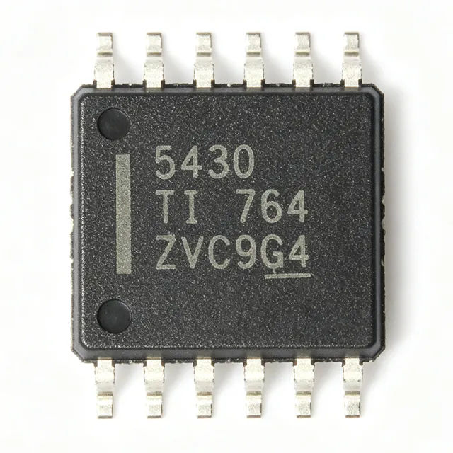
TPS5430DDAR - 3A, 36V Step-Down Converter | Texas Instruments
MPN: TPS5430DDAR ✓ 啟用中| 數量 | 單價 | 小計 |
|---|---|---|
| 1 | $2.15 | $2.15 |
| 10 | $1.93 | $19.30 |
| 100 | $1.62 | $162.00 |
| 500 | $1.38 | $690.00 |
| 1,000 | $1.19 | $1,190.00 |
TPS5430DDAR 概覽
A buck converter is a type of switching voltage regulator that efficiently steps a higher DC voltage down to a lower one using a switching MOSFET, an inductor, and output capacitors. Unlike linear regulators, switching converters routinely exceed 90% efficiency, making them the foundation of modern power management IC hierarchies (DC-DC converter -> switching regulator -> point-of-load converter). The TPS5430 belongs to TI's SWIFT family of DC-DC converters.
Key features include the 5.5V to 36V input range that directly accepts 12V and 24V industrial and automotive buses, 3A continuous output current, fixed 500kHz operation that permits small inductors, an integrated high-side N-channel MOSFET, internal loop compensation, soft-start, cycle-by-cycle current limit, and thermal shutdown. The thermally enhanced SO-8 PowerPAD package provides low thermal resistance for full-load operation without an external heatsink.
The device uses PWM voltage-mode control with an internal 1.221V bandgap reference; output voltage is set by an external resistor divider on the VSENSE pin. A bootstrap capacitor between BOOT and PH drives the high-side MOSFET gate above VIN. Fixed-frequency operation simplifies EMI filter design compared with variable-frequency converters.
Typical applications include point-of-load supplies for FPGAs, DSPs, and microcontrollers, 24V industrial bus power, telecom intermediate rails, 12V automotive accessory power, and 5V/3.3V distributed power systems.
Design tip: place input/output capacitors and the bootstrap capacitor close to the IC, solder the PowerPAD to a copper pour with thermal vias, and keep the PH switching node and power loops short to minimize ringing and EMI.
直接替換替代品,適用於 TPS5430DDAR — 相同封裝,腳位對腳位相容。需重新設計 PCB 的不同封裝零件不列入。
此系列的變體
與下列產品可直接替換的同系列型號: TPS5430DDAR (相同外形與佔位) — 差異在於 Topology, Output Voltage Range, Package, Input Voltage Range, Control Method.
快速比較工具 — 選擇替代零件進行並排比較:
TPS5430DDA
✅ 直接替換📋 參考替代品(不在目錄中)
TPS5430DDAG4
✅ 直接替換📋 參考替代品(不在目錄中)
TPS5430QDDARQ1
✅ 直接替換✗ 缺貨
$1.95 / 單位
查看資料表 →TPS5450DDAR
✅ 直接替換聯絡詢價
查看資料表 →TPS54331DR
⚡ 相同封裝聯絡詢價
查看資料表 →MP1584EN
⚡ 相同封裝📋 參考替代品(不在目錄中)
RT8279GSP
⚡ 相同封裝📋 參考替代品(不在目錄中)
TPS5430DDAR 最大額定值與電氣特性
| 拓撲 | Step-Down (Buck) |
| 輸入電壓範圍 | 5.5 V to 36 V |
| 輸出電壓 | Adjustable, 1.221 V to near VIN |
| 最大輸出電流 | 3 A |
| 切換頻率 | 500 kHz (fixed) |
| 參考電壓 | 1.221 V |
| Control Topology | Voltage-mode PWM |
| MOSFET | Integrated high-side N-channel |
| Protection Features | Cycle-by-cycle current limit, thermal shutdown, soft-start |
| 輸出數量 | 1 |
| 封裝 | 8-PowerSOIC (DDA), PowerPAD, 0.154 in / 3.90 mm width |
| 安裝類型 | Surface Mount |
| Packaging | Tape & Reel (R suffix) |
| RoHS 狀態 | Compliant |
| Family | TI SWIFT DC-DC converters |
TPS5430DDAR 腳位配置
| 腳位 1 | BOOT — Bootstrap capacitor connection to PH for high-side gate drive |
| 腳位 2 | NC/GND — No connect / ground per datasheet layout |
| 腳位 3 | VSENSE — Feedback input from output voltage divider (1.221V reference) |
| 腳位 4 | ENA — Enable input, active high |
| 腳位 5 | SS/TR — Soft-start / tracking programming pin |
| 腳位 6 | GND — Ground reference (PowerPAD also ground) |
| 腳位 7 | VIN — Input supply, 5.5V to 36V |
| 腳位 8 | PH — Phase / switch node to inductor |
典型應用
TPS5430DDAR 適用於 6 應用s: 24V Industrial Bus Point-of-Load, 12V Automotive Accessory Power, FPGA/DSP Point-of-Load Supply, Telecom Intermediate Rail Conversion, Distributed 5V/3.3V Power Systems, Battery-Powered and Portable Instrumentation.
24V Industrial Bus Point-of-Load
The TPS5430DDAR's 5.5V to 36V input range directly accepts 24V industrial control buses with transient headroom, eliminating a pre-regulator stage. Delivering 3A at a fixed 500kHz, it powers PLC I/O modules, sensors, and motor-drive logic rails. Internal compensation and fixed-frequency PWM simplify EMI filter design, while cycle-by-cycle current limit protects against shorted loads on long factory wiring. Its 1.221V reference allows any intermediate rail from 1.22V upward.
推薦
12V Automotive Accessory Power
For 12V automotive accessory rails, the 36V maximum input covers load-dump-adjacent conditions in protected front ends, and the automotive-qualified TPS5430QDDARQ1 variant (same footprint) supports AEC-Q100 programs. The 3A output supplies infotainment sub-rails, telematics, and body-electronics processors at 5V or 3.3V with efficiency above 90%, reducing thermal load in sealed enclosures. Fixed 500kHz switching keeps inductors small for space-constrained modules.
推薦
FPGA/DSP Point-of-Load Supply
The TPS5430DDAR provides 3A core and I/O rails for FPGAs, DSPs, and microcontrollers from 5V or 12V intermediates. Its soft-start pin enables controlled inrush for high ceramic capacitance, and the 500kHz fixed frequency allows inductors in the 10-15uH class with fast transient response for logic load steps. The 1.221V reference supports modern low-voltage cores, and the PowerPAD package dissipates conversion losses without a heatsink at typical 2-3A loads.
推薦
Telecom Intermediate Rail Conversion
In telecom and networking equipment, the TPS5430DDAR converts intermediate distribution voltages down to point-of-load rails with 90%+ efficiency. The 36V input tolerates -48V-derived rails after a step-down front end, and the wide input range allows one BOM across 12V, 15V, and 24V shelves. The thermal shutdown and hiccup-style current limit protect against fan-failure thermal events common in telecom cabinets, while the SO-8 PowerPAD suits high-density line-card layouts.
推薦
Distributed 5V/3.3V Power Systems
For distributed power architectures, the TPS5430DDAR generates 5V or 3.3V logic rails from upstream intermediates at a fixed 500kHz, so ripple falls in a predictable band that standard LC filters attenuate easily. Voltage-mode PWM with internal compensation reduces external component count to an inductor, two divider resistors, and input/output capacitors, cutting BOM cost. The adjustable output and 3A capacity cover backplane-fed subsystems, industrial gateways, and test-instrument auxiliaries.
推薦
Battery-Powered and Portable Instrumentation
Portable instruments powered by 12V lead-acid or multi-cell Li-ion packs benefit from the TPS5430DDAR's wide 5.5V-36V input that spans battery discharge curves. Fixed-frequency 500kHz operation keeps the converter out of audible bands and enables magnetics small enough for handheld enclosures, while better than 90% efficiency extends runtime. Thermal shutdown protects against blocked ventilation, and the SS pin can sequence the analog front end after the digital core.
推薦
推薦產品摘要
工程參考資料,適用於 TPS5430DDAR — 比較、設計指引及合規資訊。
選型指南
與替代品比較
| 參數 | 本產品 | TPS5430DDA | TPS5430QDDARQ1 | TPS5450DDAR | TPS54331DR |
|---|---|---|---|---|---|
| Package | 8-PowerSOIC (DDA) | 8-PowerSOIC (DDA) - same | 8-PowerSOIC (DDA) - same | 8-PowerSOIC (DDA) - same | SOIC-8 - different pinout |
| Brand | Texas Instruments | Texas Instruments | Texas Instruments | Texas Instruments | MPS |
| Input Voltage Range | 5.5V to 36V | 5.5V to 36V | 5.5V to 36V | 5.5V to 36V | 4.5V to 28V |
| Output Current | 3 A | 3 A | 3 A | 5 A | 1.5 A |
| Switching Frequency | 500 kHz | 500 kHz | 500 kHz | 500 kHz | 1.5 MHz (adjustable) |
| Automotive Grade | No | No | Yes (AEC-Q100) | No (Q1 version available) | No |
| Reference Voltage | 1.221 V | 1.221 V | 1.221 V | 1.221 V | 0.8 V |
| Approx. Price (1 pc, as of 2026-08-29) | $2.15 | $2.15 | $2.50 | $3.10 | $0.60 |
主要差異化特點
- Widest input range in classic SWIFT SO-8 family (對比TPS54331DR)
- Pin-compatible 5A upgrade path (對比TPS5450DDAR)
- Higher output current than cross-brand equivalents (對比MP1584EN)
- Automotive qualified variant available (對比TPS5430DDA)
設計說明
The SO-8 PowerPAD is essential to thermal performance: solder the pad to a ground pour with an array of thermal vias (typically 3x3 on 1.0mm pitch) to the internal plane. At 12Vin to 3.3V/3A out, dissipation is roughly 2W; without a solid PowerPAD connection, junction temperature can exceed limits. Follow the TI datasheet EVM thermal layout.
Keep the input capacitor, PH pin, and freewheeling diode ground loop as short and wide as possible - this is the high-di/dt hot loop. Place the BOOT capacitor (0.01uF) directly between BOOT and PH pins. Route the VSENSE feedback trace away from PH and the inductor to avoid switching noise corrupting regulation.
The PH pin switches between VIN and below ground during dead time - use an adequate external Schottky diode and do not exceed the 36V absolute maximum on VIN. Set soft-start capacitance per load capacitance to prevent current-limit foldback during startup with large ceramic output banks. Verify the resistor divider tolerance (1%) to keep output within spec.
Fixed 500kHz operation produces predictable harmonics - add a small RC snubber across PH to ground if ringing exceeds component ratings. A pi input filter may be required to meet conducted emissions on 24V industrial buses; the fixed frequency (versus variable-frequency parts like MP1584EN) makes filter design straightforward.
合規資訊
RoHS compliant per DigiKey product listing (non-G4 suffix indicates standard RoHS-compliant TI ordering). AEC-Q100 not applicable to standard part - use TPS5430QDDARQ1 for automotive qualification.





