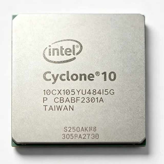
10CX105YU484I5G
10CX105YU484I5G - 104K-Cell Cyclone 10 GX FPGA | Intel | Industrial Systems
The Intel 10CX105YU484I5G is a Cyclone 10 GX field-programmable gate array (FPGA) with 104,000 logic cells, 8,640,? [DATA_NEEDED: logic elements value] embedded memory bits, and 188 user I/O elements in a 484-pin BGA package. It is designed for configurable digital logic, high-speed interfaces, and industrial applications requiring programmable hardware. The 484-pin package designation is U484, and the ordering code includes the industrial temperature grade and speed-grade identifier I5.
An FPGA is a semiconductor device whose digital logic and interconnects are configured after manufacturing. Its hierarchy is FPGA, programmable logic device, configurable logic integrated circuit, and digital semiconductor. Unlike a fixed-function ASIC, an FPGA can implement changing logic functions, interface protocols, control algorithms, and signal-processing datapaths. The Cyclone 10 GX family places programmable logic resources together with I/O and embedded functional blocks, allowing a system designer to consolidate functions that might otherwise require several connected components.
The defining feature of 10CX105YU484I5G is its 104,000-cell Cyclone 10 GX architecture. The device provides 188 user I/O resources, 8,640,? [DATA_NEEDED: embedded memory value] memory resources as reported by the distributor description, and 484 package terminals. Its FPGA structure supports configurable parallel logic, serial communication, state machines, timing logic, and custom control blocks. The exact supported transceiver count, maximum operating frequency, power supply limits, and embedded block details must be confirmed from the manufacturer datasheet before final design sign-off.
The 10CX105YU484I5G uses a 20 nm process technology, as identified in the distributor listing. This places the component in a high-density programmable-logic class aimed at designs that need more integration than a small CPLD or low-capacity FPGA. The package uses a 484-pin BGA footprint, so PCB escape routing, via-in-pad strategy, solder-mask definition, and signal-integrity analysis are important. The device should be treated as a complex high-speed digital component even where a particular design does not use every available I/O.
Typical applications include industrial control and automation, communication equipment, test and measurement, video and image processing, and custom data-acquisition systems. These applications benefit from the ability to revise logic, support multiple interface standards, and adapt timing or protocol behavior without replacing the entire PCB. The 188 I/O resources are especially relevant to systems that aggregate sensors, control signals, memory interfaces, and management buses.
When designing with this FPGA, verify all I/O-bank voltage constraints, clocking requirements, configuration architecture, power sequencing, and supported interface standards from the manufacturer documentation. The industrial-grade ordering code should be checked against the complete temperature and qualification wording in the official datasheet. This page combines verified distributor attributes, package and sourcing information, and practical engineering guidance; values not exposed by the supplied search data are explicitly marked rather than estimated.
USD $954.55
有现货