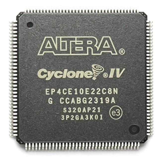
EP4CE10E22C7
EP4CE10E22C7 - 10,320-LC Cyclone IV E FPGA | Intel
The Intel/Altera EP4CE10E22C7 is a Cyclone IV E field-programmable gate array with 10,320 logic cells, 91 user I/O, a 1.2 V supply, and a 144-pin exposed-pad EQFP package. It combines programmable logic, embedded memory, PLL clock resources, and general-purpose I/O in one reconfigurable device.
A field-programmable gate array, or FPGA, is a semiconductor whose digital circuitry is configured after manufacture. An FPGA belongs to the programmable-logic hierarchy, combining LUT-based combinational logic, flip-flops, routing, block memory, and clock-management resources. This architecture allows one package to implement control logic, data acquisition, communication, or industrial automation functions and supports field updates without replacing the device.
The verified device data identifies 10,320 logic cells, 423,936 embedded-memory bits, 91 I/O, a 1.2 V nominal supply, and a 144-pin EQFP package. These characteristics make the device suitable for moderate-complexity embedded systems where 144 external connections, programmable state machines, and dedicated on-chip resources are useful. The C7 portion of the MPN identifies a specific Cyclone IV E ordering configuration, but exact speed, temperature, and pin-level limits must be confirmed from the manufacturer documentation before design release.
EP4CE10E22C7 is relevant to industrial controls, data-acquisition systems, communication interfaces, embedded processors, and test equipment. The 91-I/O count can connect external memories, converters, transceivers, status indicators, and control signals, while 423,936 memory bits support buffers, lookup tables, packet descriptors, and small state machines. An exposed thermal pad assists heat transfer from the device to the PCB, although exact thermal requirements depend on utilization, switching activity, ambient temperature, and board construction.
Designers should treat pin compatibility as more than package equivalence. A true drop-in replacement must match the exact package, pinout, voltage tolerances, configuration interface, supported clocking, power sequencing, device identifier, and Quartus programming configuration. Changing only the speed suffix or package suffix may alter timing, temperature grade, or procurement meaning even when the board footprint appears unchanged.
The most important procurement step is configuration matching. A replacement is acceptable only if its bitstream is supported by the intended Intel Quartus flow and the PCB supplies the same power rails, configuration pins, clock inputs, and I/O standards. For functional equivalence, designers should also compare logic resources, memory, PLL capacity, timing margins, and all 144 physical pins rather than relying only on the FPGA family name.
This page combines the verified 10,320-cell, 91-I/O, 1.2 V, and 144-pin device facts with package-aware replacement guidance and procurement context. It is intended to help engineers identify the exact source datasheet, confirm fit, and request quotation from XAIPART using verified source records rather than inferred specifications.
询价
联系我们