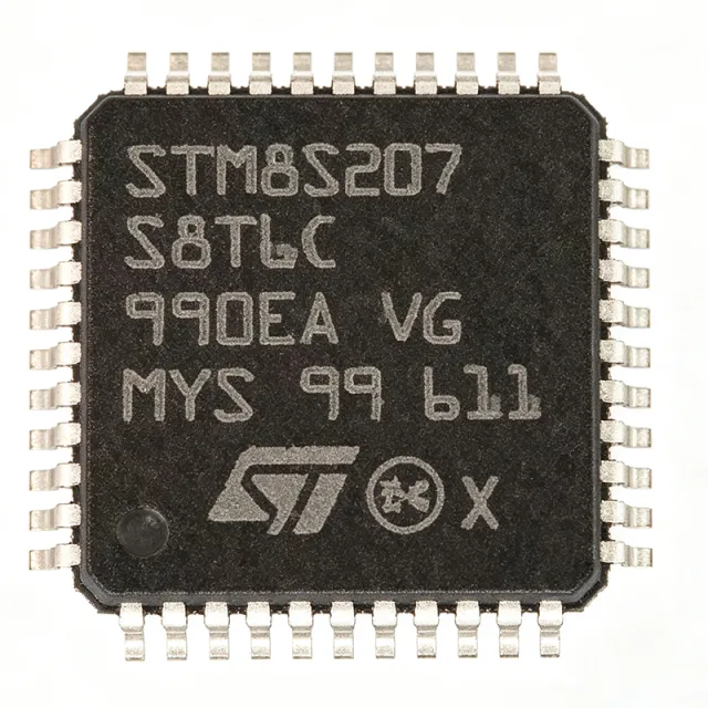
STM8S207C8T3
STM8S207C8T3 - 24MHz 8-Bit MCU with 64KB Flash | ST
The STMicroelectronics STM8S207C8T3 is an 8-bit STM8 performance-line microcontroller with a 24 MHz clock, 64 KB of Flash program memory, and a 48-LQFP 7 x 7 mm package. The supplied distributor data identifies an 8-bit architecture and confirms 64 KB Flash; Mouser additionally lists 4 KB RAM. Designed as a compact embedded-control MCU, it combines mixed-signal measurement, communications, timing, and general-purpose I/O capabilities for cost-sensitive industrial and consumer equipment.
An STM8S microcontroller belongs to the 8-bit MCU hierarchy: microprocessor core, embedded controller, and programmable digital control component. Unlike a discrete logic controller, an MCU integrates firmware memory, data memory, peripherals, and I/O in one package. This integration lets a design acquire sensor inputs, execute control logic, drive outputs, and exchange data with other assemblies without requiring several separate logic devices.
Confirmed features include 24 MHz operation, 64 KB Flash, 4 KB RAM, 38 I/O ports, and a 3 V to 5.5 V supply range. The STM8S207 family description also identifies a 10-bit ADC, timers, two UARTs, SPI, I2C, and CAN. These interfaces support analog measurement, actuator control, serial peripherals, industrial networking, and service communications. The exact pin assignments and complete electrical limits require confirmation against the manufacturer documentation.
At a maximum 24 MHz clock, the 8-bit MCU provides useful processing throughput without an external memory interface. Its 64 KB Flash supports embedded application code, while 4 KB RAM handles working data and stack operations. The 48-LQFP package exposes substantially more I/O than smaller packages, making the device suitable for connectorized control boards that need numerous digital, analog, and communications signals.
Typical uses include industrial control modules, motor and relay-control boards, sensor acquisition units, CAN-connected equipment, communication bridges, and compact consumer appliances. A design can place the MCU beside sensors and power stages, then use its ADC and serial interfaces to acquire measurements while timers and GPIO control the system. Firmware and external circuitry still require validation for timing, analog accuracy, and EMC requirements.
The principal layout consideration is careful decoupling and signal grouping around the 48-LQFP device. Keep the MCU supply path compact, place stable bypass capacitance at its supply pins, reserve adjacent routing for sensitive analog inputs, and separate high-current switching returns. Before layout approval, verify every ball-and-pad-style LQFP pin assignment against the official pinout and confirm oscillator, debug, reset, and communications routing requirements.
This page consolidates verified distributor specifications, sourcing information, family capabilities, and practical selection considerations. It distinguishes confirmed STM8S207C8T3 values from unavailable details rather than estimating electrical limits, package pricing tiers, pin functions, or lifecycle compliance claims.
询价
联系我们