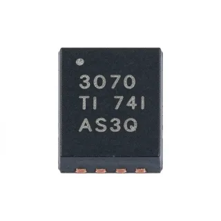
ADP2102YCPZ-1.37R7 - 600mA 1.375V Buck Converter | Analog Devices
料号: ADP2102YCPZ-1.37R7 ✓ 量产中ADP2102YCPZ-1.37R7 概述
A synchronous buck converter, or step-down regulator, reduces a higher DC input voltage to a lower regulated rail using a switching stage and an inductor. It belongs to the DC-DC converter hierarchy within power-management ICs. The ADP2102 is optimized for low-duty-cycle loads, including USB-powered systems and submicron, subvolt processor cores that require compact, efficient power conversion.
Key features include a fixed 1.375V output option, a 2.7V to 5.5V input-voltage range, up to 600mA maximum load current, and a 3MHz typical operating frequency. It requires only three external components and consumes 0.01μA in shutdown mode. Its low-ESR, low-ESL ceramic-capacitor compatibility supports designs with low output-voltage ripple.
The ADP2102 uses synchronous step-down conversion to reduce switching losses and support high efficiency. At 3MHz, its compact implementation is suited to space-constrained portable equipment. The low-duty-cycle capability also makes it relevant to processor rails where the regulator is expected to operate at a small fraction of its rated output current during normal use.
Typical applications include USB-connected portable electronics, low-voltage processor cores, mobile-device power rails, battery-powered equipment, compact industrial controllers, and USB 5V input systems. In these systems, the 1.375V fixed output directly supports low-voltage digital loads without requiring an external adjustable-feedback network.
Designers should verify the converter's operating mode, startup behavior, and external component requirements against the ADP2102 datasheet. Low-ESR ceramic input and output capacitors should be placed close to their pins, while the inductor must be selected for the intended output current, ripple requirement, and 3MHz operating frequency.
This product page combines manufacturer specifications, verified distributor listings, same-family replacement options, application guidance, and practical design notes to provide a compact engineering reference for the ADP2102YCPZ-1.37R7.
直接替换替代料: ADP2102YCPZ-1.37R7 ——相同封装,引脚兼容。需要 PCB 改动的不同封装料号已排除。
ADP2102YCPZ-1.37-R7
✅ 直接替换 ⚠️ 规格未核验📋 参考替代料(不在目录中)
ADP2102YCPZ-1.2-R7
✅ 直接替换📋 参考替代料(不在目录中)
ADP2102YCPZ-4-R7
✅ 直接替换📋 参考替代料(不在目录中)
ADP2102YCPZ-1-R7
✅ 直接替换📋 参考替代料(不在目录中)
ADP2102YCPZ-1.0-R7
✅ 直接替换📋 参考替代料(不在目录中)
ADP2102YCPZ-1.37R7 最大额定值与电气特性
| Product Type | Synchronous step-down DC-DC converter |
| Fixed Output Voltage | 1.375 V |
| 输入电压范围 | 2.7 V to 5.5 V |
| 最大输出电流 | 600 mA |
| Typical Switching Frequency | 3 MHz |
| Maximum Efficiency | 95% |
| Output Voltage Accuracy | 1% |
| Shutdown Supply Current | 0.01 μA |
| External Component Count | 3 components |
| 工作温度范围 | -40°C to +85°C |
| 封装 | 8-lead LFCSP |
| Package Dimensions | 3 mm × 3 mm |
| 安装类型 | Surface Mount |
| 拓扑 | Buck |
| 输出数量 | 1 |
| 输出类型 | Fixed |
| Adjustable Output Voltage Range | 1.5 V to 3.3 V |
| Capacitor Compatibility | Low-ESR and low-ESL ceramic capacitors |
| RoHS 状态 | Compliant |
ADP2102YCPZ-1.37R7 3 mm × 3 mm 引脚配置指南
ADP2102YCPZ-1.37R7(3 mm × 3 mm 封装)的引脚配置。 该功率器件具有栅极、漏极和源极端子。对于无极性封装,请参阅制造商数据手册以了解确切的引脚 1 方向和封装尺寸细节。常见应用包括电源设计、电机驱动和负载开关。

暂无详细引脚数据: ADP2102YCPZ-1.37R7.
请参阅 数据手册 以查看完整引脚配置。
典型应用
ADP2102YCPZ-1.37R7 适用于 6 应用s: USB-Powered Portable Electronics, Low-Voltage Processor Cores, Battery-Powered IoT Equipment, Compact Industrial Control Modules, USB 5V Interface Equipment, Mobile and Wearable Accessories.
USB-Powered Portable Electronics
The ADP2102YCPZ-1.37R7 is suitable for a USB-connected portable device requiring a compact 1.375V rail from a 2.7V to 5.5V input. Its 600mA maximum output, 3MHz typical switching frequency, and low-duty-cycle capability align with USB applications and 5V systems described by Analog Devices. Placing the converter between the 5V USB supply and a subvolt processor core reduces the available rail while retaining synchronous-converter efficiency of up to 95%. The 8-lead LFCSP also limits board area, although the inductor and low-ESR ceramic capacitors require careful layout close to the regulator.
推荐
Low-Voltage Processor Cores
The ADP2102YCPZ-1.37R7 can generate a regulated 1.375V processor-core rail from a 2.7V to 5.5V source. Its 600mA rating provides useful headroom for compact processors and other digital logic, while the 3MHz switching frequency supports a small implementation. The fixed output eliminates the feedback-divider selection associated with an adjustable variant. Because processor current can vary rapidly, layout must minimize parasitic inductance and use the low-ESR, low-ESL capacitors supported by the ADP2102 family. Thermal and current checks remain necessary when the operating duty cycle approaches the rated 600mA.
推荐
Battery-Powered IoT Equipment
The ADP2102YCPZ-1.37R7 is appropriate for battery-powered IoT equipment that needs a regulated low-voltage rail from a 2.7V to 5.5V source. Its synchronous topology supports conversion efficiency up to 95%, which is valuable when energy consumption limits operating time. The 0.01μA shutdown supply current provides a low-power state when the equipment is inactive. Low duty cycle is particularly relevant when a sensor system spends most of its time asleep and wakes for short processing intervals. The converter should be paired with an inductor and ceramic capacitors that meet the datasheet requirements without adding excessive board area.
推荐
Compact Industrial Control Modules
The ADP2102YCPZ-1.37R7 can support a 1.375V digital rail in compact industrial control modules operating from a 3.3V or 5V input. Its specified -40°C to +85°C temperature range covers common industrial environments, and its 600mA output rating serves low-power controllers, logic, and interface sections. The 3MHz operating frequency reduces the size of the external inductor and filtering network relative to many lower-frequency converters. Designers should preserve the manufacturer’s recommended capacitor layout, account for inductor saturation at maximum load, and verify transient performance across the expected input range and switching states.
推荐
USB 5V Interface Equipment
The ADP2102YCPZ-1.37R7 is well suited to USB 5V interface equipment requiring a lower, regulated supply for a controller or transceiver section. The Analog Devices data sheet identifies low-duty-cycle capability as ideal for USB applications, and the 2.7V to 5.5V input range accepts the nominal 5V source while accommodating downstream supply variation. Synchronous operation provides up to 95% efficiency, while the fixed 1.375V output avoids resistor-setpoint variation. Correct implementation requires low-ESR input and output capacitors placed close to the device, an inductor sized for the 600mA maximum current, and a layout that limits switching-node coupling to sensitive interface circuitry.
推荐
Mobile and Wearable Accessories
The ADP2102YCPZ-1.37R7 can provide a compact 1.375V supply for mobile accessories, wearable electronics, and portable sensor assemblies. Its 8-lead LFCSP package, 3MHz switching frequency, and three-external-component implementation support space-constrained layouts. The fixed 1.375V output is useful for low-voltage digital subsystems, while the 600mA maximum current accommodates small processing and communication loads. Shutdown current of 0.01μA supports battery conservation between active periods. Product-level thermal and transient validation remains important because sustained conversion loss depends on the input-to-output voltage difference and load duty cycle.
推荐
推荐产品汇总
工程参考数据: ADP2102YCPZ-1.37R7 ——对比、设计指导和合规信息。
选型指南
与替代料对比
| 参数 | 本产品 | ADP2102YCPZ-1.37-R7 | ADP2102YCPZ-1.2-R7 | ADP2102YCPZ-4-R7 | ADP2102YCPZ-1-R7 |
|---|---|---|---|---|---|
| Brand | Analog Devices | Analog Devices | Analog Devices | Analog Devices | Analog Devices |
| Package | 8-lead LFCSP | 8-lead LFCSP - same | 8-lead LFCSP - same | 8-lead LFCSP - same | 8-lead LFCSP - same |
| Output Voltage | 1.375 V fixed | 1.375 V fixed | 1.2 V fixed | 4 V fixed | 1.5 V to 3.3 V adjustable |
| Input Voltage Range | 2.7 V to 5.5 V | 2.7 V to 5.5 V | 2.7 V to 5.5 V | 2.7 V to 5.5 V | 2.7 V to 5.5 V |
| Maximum Output Current | 600 mA | 600 mA | 600 mA | 600 mA | 600 mA |
| Typical Switching Frequency | 3 MHz | 3 MHz | 3 MHz | 3 MHz | 3 MHz |
| Maximum Efficiency | 95% | 95% | 95% | 95% | 95% |
| Output Voltage Accuracy | 1% | 1% | 1% | 1% | 1% |
| Shutdown Supply Current | 0.01 μA | 0.01 μA | 0.01 μA | 0.01 μA | 0.01 μA |
| Output Configuration | Fixed | Fixed | Fixed | Fixed | Adjustable |
关键差异点
- Provides the required intermediate 1.375V fixed rail (对比 ADP2102YCPZ-1.2-R7)
- Supports higher output conversion than the 1.2V fixed variant (对比 ADP2102YCPZ-1.2-R7)
- Fixed output avoids feedback-resistor selection (对比 ADP2102YCPZ-1-R7)
- Higher output voltage than the 1.0V fixed option (对比 ADP2102YCPZ-1.0-R7)
设计说明
Place the ADP2102 input and output ceramic capacitors as close as practical to their corresponding pins. The Analog Devices data sheet specifically supports low-ESR, low-ESL ceramic capacitors and notes their suitability for tight output-ripple requirements. Keep the high-current switching path compact, provide a continuous ground reference beneath the exposed pad, and avoid routing the switching node beneath sensitive signal traces.
Select the inductor for the 3MHz operating frequency, 600mA maximum output current, and the acceptable ripple current. Verify saturation current, DC resistance, and the switching-loss contribution rather than relying on nominal inductance alone. Since the ADP2102 is optimized for low-duty-cycle loads, validate both startup and worst-case steady-state current rather than designing only for the average operating load.
Do not treat every ADP2102 output-voltage option as an interchangeable replacement. ADP2102YCPZ-1.37R7 produces 1.375V, while ADP2102YCPZ-1.2-R7 produces 1.2V and ADP2102YCPZ-4-R7 produces 4V. The fixed-voltage parts share the family package, but the rail value must satisfy the load's operating limits and the source must provide sufficient conversion headroom.
Keep the regulator, inductor, input capacitor, and output capacitor in one compact power-conversion area. Route the switch node to a minimum area and keep it away from feedback, analog, communication, and clock signals. Use the exposed thermal-pad connection and ground plane to remove heat, while checking that the assembled copper and neighboring components maintain adequate spacing for the package's production requirements.
合规信息
RoHS compliance is identified by a verified distributor result. The supplied data does not establish REACH, halogen-free, conflict-minerals, or automotive qualification status. AEC-Q100 is not applicable based on the supplied product information.