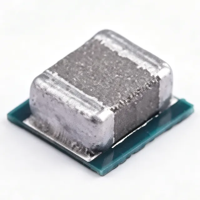
TPS82130SILR - 17V 3A 降压 MicroSiP 模块 | Texas Instruments
料号: TPS82130SILR ✓ 量产中| 数量 | 单价 | 小计 |
|---|---|---|
| 1 | $3.44 | $3.44 |
| 10 | $3.1 | $31.00 |
| 100 | $2.75 | $275.00 |
| 500 | $2.45 | $1,225.00 |
| 1,000 | $2.18 | $2,180.00 |
TPS82130SILR 概述
降压转换器,也称为 buck 转换器,是一种开关型 DC-DC 电压调节器,可将较高的输入电压高效转换为较低的输出电压。降压转换器是电源管理 IC 层级中的核心构建模块,与 LDO、电荷泵和电源模块并列。TPS82130 进一步将分立开关 FET、电感和环路补偿集成到单个微型模块中,与需要外部 FET、功率电感和补偿组件的分立稳压器设计相比,大幅减少了外部元件数量和 PCB 面积。
主要特性包括:支持 12V 和 5V 总线系统的宽 3V-17V 输入范围、3A 连续输出、通过外部电阻分压器实现 0.9V-5V 可调输出、2.2MHz 固定开关频率(允许使用小型外部电容)、用于限制浪涌电流的内部软启动、用于时序控制的电源良好输出标志、用于关断控制的使能引脚以及热关断保护。MicroSiP 封装具有底部散热焊盘,可将热量直接传导至 PCB 铜箔。
在技术上,TPS82130 采用固定频率峰值电流模式控制,以最小的输出电容(通常为 22uF 陶瓷电容)提供快速瞬态响应和稳定性。它支持 100% 占空比操作,可在高 VIN 至 VOUT 比下实现低压差。集成屏蔽电感降低了辐射 EMI,同时简化了 PCB 布局,1.5mm 的低高度适合使用标准表面贴装设备进行自动化组装。
典型应用包括工业系统中 FPGA、DSP 和 ASIC 的负载点 (POL) 电源、工厂自动化传感器供电、IoT 边缘节点中的 12V 轨分布式电源,以及解决方案尺寸至关重要的便携式测试设备。
设计时,请遵循数据手册关于输入和输出陶瓷电容的建议,将模块靠近负载放置,并在散热焊盘下方提供充足的铜面积,尤其是在高输出电流时。价格参考适用于 2026-08-28。
本页面综合了分销商定价、直接替代方案以及制造商数据手册中未包含的实用设计说明。
直接替换替代料: TPS82130SILR ——相同封装,引脚兼容。需要 PCB 改动的不同封装料号已排除。
本系列中的变体
可与以下型号直接替换的同系列型号: TPS82130SILR (相同外形与封装尺寸) ——差异在于 Continuous Output Current, MSL Level, Output Voltage Range, Package, Switching Frequency.
快速对比工具——选择替代料号进行并排对比:
TPS82140SILR
✅ 直接替换✓ 有现货
$2.45 / 个
查看数据手册 →TPS82150SILR
✅ 直接替换📋 参考替代料(不在目录中)
TPS82130SILT
✅ 直接替换📋 参考替代料(不在目录中)
TPS82130SILR 最大额定值与电气特性
| 拓扑 | Synchronous Buck (Step-Down) |
| Module Type | MicroSiP Power Module (integrated inductor and FETs) |
| 输入电压范围 | 3 V to 17 V |
| 输出电压范围 | 0.9 V to 5 V (adjustable) |
| Continuous Output Current | 3 A |
| 开关频率 | 2.2 MHz (typical, fixed) |
| Control Mode | Peak Current Mode |
| Efficiency (typical) | >90% at moderate load |
| 软启动 | Internal |
| 电源正常输出 | Yes |
| 使能引脚 | Yes (active-high) |
| 热关断 | Yes |
| 工作温度范围 | -40C to +125C |
| 封装 | 8-pin uSIP (SIL) 3.0mm x 2.8mm x 1.5mm |
| 安装类型 | Surface Mount |
| MSL 等级 | 2 (1 year floor life) |
| RoHS 状态 | Compliant |
TPS82130SILR 引脚配置
| 引脚 1 | VIN — Input supply voltage |
| 引脚 2 | GND — Signal ground |
| 引脚 3 | EN — Enable input (active high) |
| 引脚 4 | PGND — Power ground |
| 引脚 5 | FB — Feedback voltage input |
| 引脚 6 | VOUT — Regulated output voltage |
| 引脚 7 | PG — Power good output flag |
| 引脚 8 | AGND — Analog ground |
典型应用
TPS82130SILR 适用于 6 应用s: FPGA Point-of-Load Power, Industrial Sensor and PLC Supplies, IoT Edge Devices and Gateway Nodes, Portable Test and Measurement Equipment, DSP and ASIC Core Power, Communication Equipment Power.
FPGA Point-of-Load Power
The TPS82130SILR is an ideal point-of-load supply for FPGA core and auxiliary rails in industrial embedded systems. With 3A continuous output, 0.9V to 5V adjustable output range, and a 3.0mm x 2.8mm uSIP footprint, it can power the FPGA core (typically 1.0V-1.2V), auxiliary (1.8V), and I/O (2.5V or 3.3V) rails from a single 12V bus. The 2.2MHz switching frequency avoids interfering with common FPGA clock harmonics around 100-500MHz, eliminating beat-frequency noise issues that plague lower-frequency regulators. Integrated synchronous FETs and shielded inductor eliminate 6-8 discrete components, dramatically reducing PCB area versus discrete buck designs.
推荐
Industrial Sensor and PLC Supplies
The TPS82130SILR powers industrial 4-20mA loop transmitters, PLC analog input modules, and 24V-bus sensor conditioning circuits. Its 3V-17V input range directly accepts the 24V industrial bus (after protection/regulation) and 12V backplane rails commonly used in factory automation. The wide operating temperature range of -40C to +125C supports deployment in unconditioned factory environments. With internal thermal shutdown, power-good output, and enable pin for power sequencing, the TPS82130 provides the robustness required for industrial IEC 61010 environments. Typical efficiency above 90% minimizes thermal dissipation in sealed enclosures.
推荐
IoT Edge Devices and Gateway Nodes
The TPS82130SILR fits compact IoT edge nodes and gateway designs that require multiple voltage rails in a small footprint. The integrated MicroSiP package occupies 75% less PCB area than equivalent discrete buck designs, freeing space for wireless modules, sensors, and battery management. With 3A peak capability, the TPS82130 can power a small SoC plus Wi-Fi/BLE radio module directly from a 12V or USB-C input. The 2.2MHz switching frequency enables small ceramic output capacitors (typically 22uF), and the internal soft-start limits inrush current that could trip upstream USB current-limit switches.
推荐
Portable Test and Measurement Equipment
Handheld oscilloscopes, data loggers, and field test equipment benefit from the TPS82130SILR's compact size, high efficiency, and wide input range. Battery-powered instruments often use a 2-cell or 3-cell Li-ion pack (6V-12.6V) that maps directly to the TPS82130 input range. The 3A continuous capability powers analog front-end ADCs, FPGAs, and display backlight drivers simultaneously. The 1.5mm low-profile uSIP package allows the entire power tree to fit on the back side of small PCBs, leaving the top side for analog signal paths and user interface components. High efficiency above 90% extends battery runtime.
推荐
DSP and ASIC Core Power
The TPS82130SILR is well-suited as a POL supply for DSP, ASIC, and high-performance microcontroller core rails. Modern DSPs often require 1.0V to 1.2V at 2-3A peak current with tight transient response - the TPS82130's peak-current-mode control delivers fast transient response with minimal output capacitance. The adjustable output from 0.9V to 5V covers virtually all DSP/ASIC core voltage requirements. The integrated power-good output enables sequencing with other system rails, and the enable pin allows shutdown to microampere-level quiescent current for sleep-mode applications. According to TI datasheet, the device supports 100% duty cycle for low-dropout operation at high VIN-VOUT deltas.
推荐
Communication Equipment Power
Networking switches, wireless base stations, and small cell radio units can use the TPS82130SILR to power digital signal processors and baseband chips from 12V backplane rails. The 2.2MHz switching frequency and integrated shielded inductor minimize radiated EMI - critical for communication equipment that must meet FCC and CE conducted/radiated emissions limits. With 3A output capability, the TPS82130 powers baseband SoCs and DDR memory termination rails simultaneously. The small MicroSiP footprint allows power circuits to be placed directly beneath or adjacent to the load IC, minimizing parasitic inductance and improving transient response.
推荐
推荐产品汇总
工程参考数据: TPS82130SILR ——对比、设计指导和合规信息。
选型指南
与替代料对比
| 参数 | 本产品 | TPS82140SILR | TPS82150SILR | TPS82130SILT |
|---|---|---|---|---|
| Package | 8-pin uSIP (SIL) 3.0x2.8mm | 8-pin uSIP (SIL) 3.0x2.8mm - same | 8-pin uSIP (SIL) 3.0x2.8mm - same | 8-pin uSIP (SIL) 3.0x2.8mm - same |
| Brand | Texas Instruments | Texas Instruments | Texas Instruments | Texas Instruments |
| Output Current | 3 A | 2 A | 1 A | 3 A |
| Input Voltage Range | 3 V to 17 V | 3 V to 17 V | 3 V to 17 V | 3 V to 17 V |
| Output Voltage Range | 0.9 V to 5 V | 0.9 V to 5 V | 0.9 V to 5 V | 0.9 V to 5 V |
| Switching Frequency | 2.2 MHz | 2.2 MHz | 2.2 MHz | 2.2 MHz |
| Module Type | MicroSiP (integrated inductor) | MicroSiP (integrated inductor) | MicroSiP (integrated inductor) | MicroSiP (integrated inductor) |
关键差异点
- TPS821xx uSIP 系列中最高输出电流 (对比 TPS82140SILR)
- 相同封装尺寸,较低电流用于降低成本设计 (对比 TPS82150SILR)
- 集成 MicroSiP 封装省去 6-8 个分立元件 (对比 分立 TPS54360 降压设计)
设计说明
估算:在 VIN=12V、VOUT=3.3V 和 3A 负载下,TPS82130SILR 耗散约 (12-3.3) x 3 = 26.1 W 的功率。为底部散热焊盘提供足够的铜箔(数据手册建议最小焊盘图案),结至环境热阻通常约为 30-40 C/W,导致高于环境温度 50-80 C 的温升。对于连续 3A 操作,请严格遵循数据手册参考布局图案,并在封装外露焊盘下方使用多个散热过孔将热量传导至 PCB 内层。
将 TPS82130SILR 模块靠近负载 IC 放置,最好在 5-10mm 以内,以最小化输出环路中的寄生电感。在 VIN、VOUT、PGND 和外露散热焊盘上使用宽铜箔(至少 50mil)。根据 TI 数据手册布局指南,将输入陶瓷电容(通常为 22uF X7R)尽可能靠近 VIN 引脚放置,并将输出陶瓷电容(通常为 22uF X7R)直接放置在 VOUT 引脚处。AGND 引脚应在输出电容接地回路附近的单点连接到 PGND 铜箔。
请勿在超过 17V 绝对最大 VIN 的情况下操作 TPS82130SILR - 12V 工业总线上的瞬态在热插拔事件期间可能超过此值。如果设计连接到长外部电缆,请添加 TVS 二极管或输入电压钳位。请勿省略输入电容:TPS82130 的高 di/dt 开关需要低 ESR 陶瓷输入电容以防止 VIN 振铃。根据数据手册,使用 X7R/X5R 陶瓷电容 - 不要用 Y5V 替代,后者在直流偏置和温度下会损失 60-80% 的标称电容。
使 FB(反馈)走线远离噪声开关节点(VIN、PGND、VOUT),并使用短而窄的走线从输出电容顶部直接布线到 FB 引脚,周围环绕接地铜箔。请勿将反馈分压电阻放置在电感附近 - 磁耦合会向反馈路径注入噪声,导致输出纹波或不稳定。PG(电源良好)输出是开漏信号,需要外部上拉电阻(通常为 10k-100k)连接到 VOUT 或逻辑电源轨。
合规信息
RoHS and REACH compliant per TI product page. Not AEC-Q100 qualified; choose TPS62150A-Q1 or similar -Q1 part for automotive applications.







