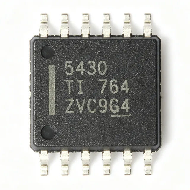
TPS5430DDAR - 3A、36V 降压转换器 | Texas Instruments
料号: TPS5430DDAR ✓ 量产中| 数量 | 单价 | 小计 |
|---|---|---|
| 1 | $2.15 | $2.15 |
| 10 | $1.93 | $19.30 |
| 100 | $1.62 | $162.00 |
| 500 | $1.38 | $690.00 |
| 1,000 | $1.19 | $1,190.00 |
TPS5430DDAR 概述
降压转换器是一种开关电压稳压器,利用开关 MOSFET、电感和输出电容将较高的直流电压高效降至较低电压。与线性稳压器不同,开关转换器的效率通常超过 90%,使其成为现代电源管理 IC 层级(DC-DC 转换器 -> 开关稳压器 -> 负载点转换器)的基础。TPS5430 属于 TI 的 SWIFT 系列 DC-DC 转换器。
主要特性包括:5.5V 至 36V 输入范围,可直接接受 12V 和 24V 工业及汽车总线;3A 连续输出电流;固定 500kHz 工作频率,允许使用小电感;集成高侧 N 沟道 MOSFET;内部环路补偿;软启动;逐周期电流限制;以及热关断。热增强型 SO-8 PowerPAD 封装提供低热阻,可在无外部散热器的情况下满负载运行。
该器件采用 PWM 电压模式控制,内置 1.221V 带隙基准;输出电压由 VSENSE 引脚上的外部电阻分压器设定。BOOT 与 PH 之间的自举电容将高侧 MOSFET 栅极驱动至 VIN 以上。与可变频率转换器相比,固定频率工作简化了 EMI 滤波器设计。
典型应用包括 FPGA、DSP 和微控制器的负载点电源,24V 工业总线电源,电信中间轨,12V 汽车附件电源,以及 5V/3.3V 分布式电源系统。
设计提示:将输入/输出电容和自举电容靠近 IC 放置,将 PowerPAD 焊接至带散热过孔的铜箔,并保持 PH 开关节点和功率回路短小,以最小化振铃和 EMI。
直接替换替代料: TPS5430DDAR ——相同封装,引脚兼容。需要 PCB 改动的不同封装料号已排除。
本系列中的变体
可与以下型号直接替换的同系列型号: TPS5430DDAR (相同外形与封装尺寸) ——差异在于 Topology, Output Voltage Range, Package, Input Voltage Range, Control Method.
快速对比工具——选择替代料号进行并排对比:
TPS5430DDA
✅ 直接替换📋 参考替代料(不在目录中)
TPS5430DDAG4
✅ 直接替换📋 参考替代料(不在目录中)
TPS5430QDDARQ1
✅ 直接替换✓ 有现货
$1.95 / 个
查看数据手册 →TPS5450DDAR
✅ 直接替换✓ 有现货
$2.55 / 个
查看数据手册 →TPS54331DR
⚡ 相同封装✓ 有现货
$0.85 / 个
查看数据手册 →MP1584EN
⚡ 相同封装📋 参考替代料(不在目录中)
RT8279GSP
⚡ 相同封装📋 参考替代料(不在目录中)
TPS5430DDAR 最大额定值与电气特性
| 拓扑 | Step-Down (Buck) |
| 输入电压范围 | 5.5 V to 36 V |
| 输出电压 | Adjustable, 1.221 V to near VIN |
| 最大输出电流 | 3 A |
| 开关频率 | 500 kHz (fixed) |
| 基准电压 | 1.221 V |
| Control Topology | Voltage-mode PWM |
| MOSFET | Integrated high-side N-channel |
| Protection Features | Cycle-by-cycle current limit, thermal shutdown, soft-start |
| 输出数量 | 1 |
| 封装 | 8-PowerSOIC (DDA), PowerPAD, 0.154 in / 3.90 mm width |
| 安装类型 | Surface Mount |
| Packaging | Tape & Reel (R suffix) |
| RoHS 状态 | Compliant |
| Family | TI SWIFT DC-DC converters |
TPS5430DDAR 引脚配置
| 引脚 1 | BOOT — Bootstrap capacitor connection to PH for high-side gate drive |
| 引脚 2 | NC/GND — No connect / ground per datasheet layout |
| 引脚 3 | VSENSE — Feedback input from output voltage divider (1.221V reference) |
| 引脚 4 | ENA — Enable input, active high |
| 引脚 5 | SS/TR — Soft-start / tracking programming pin |
| 引脚 6 | GND — Ground reference (PowerPAD also ground) |
| 引脚 7 | VIN — Input supply, 5.5V to 36V |
| 引脚 8 | PH — Phase / switch node to inductor |
典型应用
TPS5430DDAR 适用于 6 应用s: 24V Industrial Bus Point-of-Load, 12V Automotive Accessory Power, FPGA/DSP Point-of-Load Supply, Telecom Intermediate Rail Conversion, Distributed 5V/3.3V Power Systems, Battery-Powered and Portable Instrumentation.
24V Industrial Bus Point-of-Load
The TPS5430DDAR's 5.5V to 36V input range directly accepts 24V industrial control buses with transient headroom, eliminating a pre-regulator stage. Delivering 3A at a fixed 500kHz, it powers PLC I/O modules, sensors, and motor-drive logic rails. Internal compensation and fixed-frequency PWM simplify EMI filter design, while cycle-by-cycle current limit protects against shorted loads on long factory wiring. Its 1.221V reference allows any intermediate rail from 1.22V upward.
推荐
12V Automotive Accessory Power
For 12V automotive accessory rails, the 36V maximum input covers load-dump-adjacent conditions in protected front ends, and the automotive-qualified TPS5430QDDARQ1 variant (same footprint) supports AEC-Q100 programs. The 3A output supplies infotainment sub-rails, telematics, and body-electronics processors at 5V or 3.3V with efficiency above 90%, reducing thermal load in sealed enclosures. Fixed 500kHz switching keeps inductors small for space-constrained modules.
推荐
FPGA/DSP Point-of-Load Supply
The TPS5430DDAR provides 3A core and I/O rails for FPGAs, DSPs, and microcontrollers from 5V or 12V intermediates. Its soft-start pin enables controlled inrush for high ceramic capacitance, and the 500kHz fixed frequency allows inductors in the 10-15uH class with fast transient response for logic load steps. The 1.221V reference supports modern low-voltage cores, and the PowerPAD package dissipates conversion losses without a heatsink at typical 2-3A loads.
推荐
Telecom Intermediate Rail Conversion
In telecom and networking equipment, the TPS5430DDAR converts intermediate distribution voltages down to point-of-load rails with 90%+ efficiency. The 36V input tolerates -48V-derived rails after a step-down front end, and the wide input range allows one BOM across 12V, 15V, and 24V shelves. The thermal shutdown and hiccup-style current limit protect against fan-failure thermal events common in telecom cabinets, while the SO-8 PowerPAD suits high-density line-card layouts.
推荐
Distributed 5V/3.3V Power Systems
For distributed power architectures, the TPS5430DDAR generates 5V or 3.3V logic rails from upstream intermediates at a fixed 500kHz, so ripple falls in a predictable band that standard LC filters attenuate easily. Voltage-mode PWM with internal compensation reduces external component count to an inductor, two divider resistors, and input/output capacitors, cutting BOM cost. The adjustable output and 3A capacity cover backplane-fed subsystems, industrial gateways, and test-instrument auxiliaries.
推荐
Battery-Powered and Portable Instrumentation
Portable instruments powered by 12V lead-acid or multi-cell Li-ion packs benefit from the TPS5430DDAR's wide 5.5V-36V input that spans battery discharge curves. Fixed-frequency 500kHz operation keeps the converter out of audible bands and enables magnetics small enough for handheld enclosures, while better than 90% efficiency extends runtime. Thermal shutdown protects against blocked ventilation, and the SS pin can sequence the analog front end after the digital core.
推荐
推荐产品汇总
工程参考数据: TPS5430DDAR ——对比、设计指导和合规信息。
选型指南
与替代料对比
| 参数 | 本产品 | TPS5430DDA | TPS5430QDDARQ1 | TPS5450DDAR | TPS54331DR |
|---|---|---|---|---|---|
| Package | 8-PowerSOIC (DDA) | 8-PowerSOIC (DDA) - same | 8-PowerSOIC (DDA) - same | 8-PowerSOIC (DDA) - same | SOIC-8 - different pinout |
| Brand | Texas Instruments | Texas Instruments | Texas Instruments | Texas Instruments | MPS |
| Input Voltage Range | 5.5V to 36V | 5.5V to 36V | 5.5V to 36V | 5.5V to 36V | 4.5V to 28V |
| Output Current | 3 A | 3 A | 3 A | 5 A | 1.5 A |
| Switching Frequency | 500 kHz | 500 kHz | 500 kHz | 500 kHz | 1.5 MHz (adjustable) |
| Automotive Grade | No | No | Yes (AEC-Q100) | No (Q1 version available) | No |
| Reference Voltage | 1.221 V | 1.221 V | 1.221 V | 1.221 V | 0.8 V |
| Approx. Price (1 pc, as of 2026-08-29) | $2.15 | $2.15 | $2.50 | $3.10 | $0.60 |
关键差异点
- 经典 SWIFT SO-8 系列中最宽的输入范围 (对比 TPS54331DR)
- 引脚兼容的 5A 升级路径 (对比 TPS5450DDAR)
- 输出电流高于跨品牌等效产品 (对比 MP1584EN)
- 提供汽车级认证变体 (对比 TPS5430DDA)
设计说明
SO-8 PowerPAD 对热性能至关重要:将焊盘焊接至接地铜箔,并通过阵列散热过孔(通常 3x3,1.0mm 间距)连接至内部平面。在 12Vin 至 3.3V/3A 输出时,功耗约为 2W;若无坚实的 PowerPAD 连接,结温可能超限。遵循 TI 数据手册 EVM 热布局。
保持输入电容、PH 引脚和续流二极管接地回路尽可能短而宽——这是高 di/dt 热回路。将 BOOT 电容(0.01uF)直接放置在 BOOT 和 PH 引脚之间。将 VSENSE 反馈走线远离 PH 和电感,以避免开关噪声干扰稳压。
PH 引脚在死区时间内在 VIN 和地以下之间切换——使用足够的外部肖特基二极管,且不要超过 VIN 的 36V 绝对最大值。根据负载电容设置软启动电容,以防止启动时大容量陶瓷输出电容组导致电流限制折返。验证电阻分压器容差(1%)以保持输出在规格范围内。
固定 500kHz 工作产生可预测的谐波——如果振铃超过元件额定值,在 PH 至地之间添加小型 RC 缓冲器。在 24V 工业总线上可能需要 pi 输入滤波器以满足传导发射要求;固定频率(相对于 MP1584EN 等可变频率器件)使滤波器设计简单直接。
合规信息
RoHS compliant per DigiKey product listing (non-G4 suffix indicates standard RoHS-compliant TI ordering). AEC-Q100 not applicable to standard part - use TPS5430QDDARQ1 for automotive qualification.







