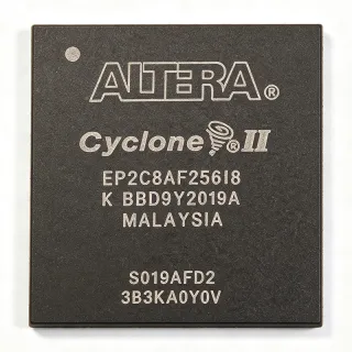
EP3C5F256C8N - Cyclone III FPGA 5K LEs 256-FBGA | Intel
料号: EP3C5F256C8N ✓ 量产中| 数量 | 单价 | 小计 |
|---|---|---|
| 1 | $17.73 | $17.73 |
| 10 | $16.1 | $161.00 |
| 100 | $13.85 | $1,385.00 |
| 500 | $12.2 | $6,100.00 |
| 1,000 | $10.95 | $10,950.00 |
EP3C5F256C8N 概述
An FPGA is a type of programmable logic device containing an array of configurable logic blocks, programmable interconnect, and embedded memory/DSP blocks that can be re-programmed in-system by manufacturers or end users after PCB assembly. Within the semiconductor taxonomy, FPGAs sit between fixed-function ASICs and software-programmable microcontrollers: they deliver hardware-level parallelism and deterministic timing while still allowing iterative logic revision. The Cyclone III family specifically targets the low-power, low-cost segment of the FPGA hierarchy (FPGA → programmable logic → PLD → digital IC), making it well suited to cost-sensitive, high-volume designs that still require hardware acceleration and parallel DSP throughput.
Key features of the EP3C5F256C8N include 5,136 logic elements organized into Logic Array Blocks (LABs), 423,936 bits of embedded memory (RAM), 23 embedded 18x18 multipliers for DSP, 4 phase-locked loops (PLLs), and 182 maximum user I/Os. The device supports multiple I/O standards including LVDS, LVTTL, LVCMOS, SSTL, and HSTL via per-bank VCCIO references. The SRAM-based configuration cells enable unlimited in-system re-programmability, and the 65 nm process technology delivers an optimal balance of logic density and static power (~0.5 mW per LE typical) for thermally constrained or battery-aware designs.
Architecturally, the device arranges its 5,136 logic elements into vertically organized LABs, interconnected by a hierarchical MultiTrack interconnect fabric with low-skew clock distribution. The 23 dedicated 18x18 multipliers enable efficient DSP operations without consuming general-purpose logic resources, supporting parallel arithmetic at clock rates up to 402 MHz internal.
Typical applications include industrial control and machine networking, video surveillance and image processing, low-cost digital signal processing, motor control and encoder interfacing, automotive telematics, serial protocol bridging (UART/SPI/I2C to high-speed interfaces), consumer electronics display controllers, and portable test and measurement equipment. The Cyclone III family's low static power makes it particularly suitable for thermally constrained or fan-less designs.
When designing with this device, ensure adequate decoupling on every PLL and core rail and ROCm decoupling on all supply rails and that the configuration mode (AS, PS, JTAG, or Fast Passive Parallel) matches the system's boot strategy. Designers migrating to newer Intel Cyclone families should plan for I/O bank voltage and pin-out differences even when targeting the same FBGA-256 footprint, and validate JTAG/AS programmer compatibility with the Quartus II toolchain.
This page synthesizes distributor pricing, same-family drop-in alternatives, and practical design considerations not consolidated in the original Altera Cyclone III handbook, giving procurement and engineering teams a single reference for the EP3C5F256C8N.
直接替换替代料: EP3C5F256C8N ——相同封装,引脚兼容。需要 PCB 改动的不同封装料号已排除。
本系列中的变体
可与以下型号直接替换的同系列型号: EP3C5F256C8N (相同外形与封装尺寸) ——差异在于 Package, Process Technology, Operating Temperature, RoHS Status, Core Voltage.
快速对比工具——选择替代料号进行并排对比:
EP3C5F256C7N
✅ 直接替换✓ 有现货
$14.2 / 个
查看数据手册 →EP3C5F256C6N
✅ 直接替换✓ 有现货
$18.85 / 个
查看数据手册 →EP3C5F256I7N
✅ 直接替换✓ 有现货
$24 / 个
查看数据手册 →EP3C5F256A7N
✅ 直接替换✓ 有现货
$24.4 / 个
查看数据手册 →EP3C5F324C8N
✅ 直接替换 ⚠️ 规格未核验📋 参考替代料(不在目录中)
EP3C5F256C8N 最大额定值与电气特性
| Series | Cyclone III |
| Device Family | Cyclone III (EP3C5) |
| Logic Elements (LEs) | 5,136 |
| Embedded Memory (bits) | 423,936 |
| Embedded Memory (Kbits) | 414 Kbits |
| Embedded 18x18 Multipliers | 23 |
| PLLs | 4 |
| Maximum User I/Os | 182 |
| Core Voltage | 1.15 V to 1.25 V |
| 工作温度 | 0C to 85C (Commercial) |
| 封装 | 256-ball FBGA (FineLine BGA) |
| Process Technology | 65 nm |
| Configuration Memory | SRAM-based (in-system reprogrammable) |
| I/O Standards Supported | LVDS, LVTTL, LVCMOS, SSTL, HSTL |
| RoHS 状态 | Lead Free (per Altera/Intel product page) |
| 安装类型 | Surface Mount |
EP3C5F256C8N 256-ball fbga (fineline bga) 引脚配置指南
EP3C5F256C8N(256-ball fbga (fineline bga) 封装)的引脚配置。 该数字 IC 包含 GPIO、通信接口(UART、SPI、I2C)和电源引脚。请参阅制造商数据手册以了解复用引脚功能和配置选项。对嵌入式系统设计和 PCB 布局至关重要。

暂无详细引脚数据: EP3C5F256C8N.
请参阅 数据手册 以查看完整引脚配置。
典型应用
EP3C5F256C8N 适用于 6 应用s: Industrial Control and Machine Networking, Video Surveillance and Image Processing, Low-Cost Digital Signal Processing, Motor Control and Encoder Interfacing, Serial Protocol Bridging, Portable Test and Measurement Equipment.
Industrial Control and Machine Networking
The EP3C5F256C8N suits industrial control and machine networking applications because its 5,136 logic elements provide enough parallelism for multiple motor-control axes, encoder interfaces, and protocol bridges on a single chip. The 4 on-chip PLLs allow independent clock synthesis for CAN, RS-485, and Ethernet PHYs without external oscillators, while 182 user I/Os easily accommodate multiple opto-isolated GPIO banks and PWM channels. With static power of roughly 0.5 mW per LE typical, the device runs cool in fan-less IP65 enclosures, and its 65 nm Cyclone III silicon is proven across decades of factory-floor deployment. Pair with EPCS16 serial configuration memory and a dedicated watchdog timer FPGA fabric block for deterministic fault recovery in PLC and SCADA systems.
推荐
Video Surveillance and Image Processing
The EP3C5F256C8N enables cost-effective video surveillance and basic image processing because its 23 dedicated 18x18 multipliers and 414 Kbits of embedded SRAM can sustain parallel FIR filtering, motion detection, and edge enhancement at common CIF/D1 rates. The 182 user I/Os accommodate parallel ITU-R BT.656 or LVDS camera inputs alongside HDMI/DVI preview outputs, while 4 PLLs generate pixel clocks for both capture and display paths. The SRAM-selectable M9K memory blocks implement line buffers and frame-difference accumulators without external SDRAM in simple motion-detection applications. For 720p/1080p pipelines, designers can add external DDR2 SDRAM and use the FPGA's controller ports as an external memory controller.
推荐
Low-Cost Digital Signal Processing
The EP3C5F256C8N is well matched to low-cost digital signal processing designs because its 23 embedded 18x18 multipliers provide approximately 23 GMACs of throughput for audio-rate and control-loop DSP at internal clock rates up to 402 MHz. The 414 Kbits of on-chip memory allow coefficient caching, and the Quartus II DSP Builder blocks accelerate FIR/IIR/FFT IP generation. Compared to microcontrollers running DSP firmware, the FPGA fabric delivers deterministic latency and parallel channel processing at similar unit cost. This makes EP3C5F256C8N a sweet spot for audio processing, power-line communication, and multi-axis servo drives where multiple control loops must execute in parallel.
推荐
Motor Control and Encoder Interfacing
The EP3C5F256C8N handles motor control and encoder interfacing because its 5,136 logic elements can implement multi-axis FOC (field-oriented control) loops, SVPWM modulators, and quadrature decoder chains concurrently without contention. The 23 dedicated 18x18 multipliers accelerate Park/Clarke transforms and PI controller arithmetic at kHz-to-MHz PWM frequencies, while the 4 PLLs synthesize the switching frequency and multiple encoder sample clocks. The 182 user I/Os accommodate Hall sensors, quadrature encoders, and isolated gate-driver interfaces for IGBT/MOSFET half-bridges. For multi-axis CNC and robotics, the FBGA-256 footprint gives board-area savings versus CPLD-plus-microcontroller solutions.
推荐
Serial Protocol Bridging
The EP3C5F256C8N excels at serial protocol bridging because its parallel logic fabric can implement multiple UART, SPI, I2C, CAN, and custom high-speed protocols on independent clock domains, all on a single chip. The 4 PLLs allow each bridge port to run on its own baud-rate clock without external oscillators, and the 182 user I/Os support voltage mixing across 3.3V, 2.5V, and 1.8V bank domains. The SRAM-selectable 414 Kbits of embedded memory implement FIFOs for rate-matching between asynchronous domains. Compared to dedicated bridge chips, EP3C5F256C8N offers flexibility to support evolving industrial protocols such as IO-Link, Modbus, and PROFINET without a re-spin of the silicon.
推荐
Portable Test and Measurement Equipment
The EP3C5F256C8N suits portable test and measurement equipment because its low static power (~0.5 mW per LE typical) extends battery runtime in handheld oscilloscopes, DMMs, and protocol analyzers. The 5,136 logic elements implement multi-channel capture, FFT analysis, and trigger logic on a single chip, while 23 dedicated 18x18 multipliers accelerate real-time FFT and digital-filter computations. The 182 user I/Os support mixed-domain probing with on-chip ADCs (where used) plus SPI-driven external ADC front-ends. The 65 nm process delivers the low-thermal profile required in sealed hand-held enclosures, and the SRAM-based configuration allows field firmware upgrades without opening the enclosure.
推荐
推荐产品汇总
工程参考数据: EP3C5F256C8N ——对比、设计指导和合规信息。
选型指南
与替代料对比
| 参数 | 本产品 | EP3C5F256C7N | EP3C5F256C6N | EP3C5F256I7N | EP3C5F256A7N | EP3C5F324C8N |
|---|---|---|---|---|---|---|
| Brand | Intel (formerly Altera) | Intel | Intel | Intel | Intel | Intel |
| Package | 256-ball FBGA | 256-ball FBGA - same | 256-ball FBGA - same | 256-ball FBGA - same | 256-ball FBGA - same | 324-ball FBGA - different |
| Logic Elements | 5,136 | 5,136 - same | 5,136 - same | 5,136 - same | 5,136 - same | 5,136 - same |
| Embedded Memory | 423,936 bits | 423,936 bits - same | 423,936 bits - same | 423,936 bits - same | 423,936 bits - same | 423,936 bits - same |
| 18x18 Multipliers | 23 | 23 - same | 23 - same | 23 - same | 23 - same | 23 - same |
| PLLs | 4 | 4 - same | 4 - same | 4 - same | 4 - same | 4 - same |
| Speed Grade | -8 | -7 (slower) | -6 (slowest) | -7 (slower) | -7 (slower) | -8 (same) |
| Operating Temperature | 0C to 85C (Commercial) | 0C to 85C (Commercial) - same | 0C to 85C (Commercial) - same | -40C to 100C (Industrial) - extended | Automotive - extended | 0C to 85C (Commercial) - same |
关键差异点
- Fastest speed grade in Cyclone III EP3C5 family (对比 EP3C5F256C7N)
- Industrial temperature grade variant available in same FBGA-256 footprint (对比 EP3C5F256I7N)
- Larger package option for higher I/O density (对比 EP3C5F324C8N)
设计说明
Estimated: at 100% logic utilization on a -8 commercial-grade EP3C5F256C8N with 1.2V core at 402 MHz, total power dissipation is approximately 1.0-1.4W (core ~0.7W + I/O ~0.4W), per typical Cyclone III power models. Designers should provide at least four 0.1uF decoupling capacitors on VCCINT and one 4.7uF bulk capacitor per VCCIO bank, plus bulk decoupling on VCCA_PLL. Use Quartus II PowerPlay early in the design cycle to size the power supply and validate thermal headroom.
The 256-ball FBGA package has a junction-to-ambient thermal resistance (theta_JA) of approximately 20 C/W with proper PCB thermal via array under the exposed pad. For designs operating above 70% utilization, design from the top-side thermal via array to inner copper planes. Estimated: at 1.4W total power, junction temperature rises approximately 28C above ambient, well within the 0C-85C commercial operating range, but industrial variants EP3C5F256I7N require additional thermal margin.
The FBGA-256 uses a 1.0 mm ball pitch with a 16x16 grid (excluding depopulated corners). Per Cyclone III handbook layout guidelines, designers must use a via-array pattern under the package center for thermal dissipation and a 4-layer PCB stack-up with continuous GND planes. JTAG chain routing should isolate TSEP, TCK, TMS, and TDO from clock signals by at least 3W line-width clearance to avoid configuration-mode noise.
Common pitfalls: (1) Selecting a configuration mode (AS/PS/JTAG/FPP) without verifying the EPCS serial configuration device compatibility - use EPCS16 or EPCS64 for EP3C5F256C8N. (2) Mixing VCCIO bank voltages without checking bank-group I/O standard compatibility. (3) Underestimating the configuration file size; the EP3C5F256C8N bitstream is typically ~1.6 Mbytes, requiring EPCS4 minimum configuration but EPCS16 is recommended for margin. (4) Forgetting to set the MSEL[2:0] pins correctly for the chosen configuration mode - MSEL float will cause AS mode boot errors.
合规信息
The 'N' suffix in EP3C5F256C8N denotes lead-free / RoHS-compliant per Altera ordering code convention. The Cyclone III family was one of the first Altera families shipped exclusively in lead-free packaging. AEC-Q100 qualification is not formally claimed for the C8N commercial variant; automotive applications should consider EP3C5F256A7N automotive speed grade.