Lattice Semiconductor

LFE2-12E-5T144I - 12K LUT ECP2 FPGA | Lattice Semiconductor

料号: LFE2-12E-5T144I ✓ 量产中
1.2 V Vdss 144-pin TQFP Package -5 Speed
最小起订量: 1 |

LFE2-12E-5T144I 概述

The Lattice Semiconductor LFE2-12E-5T144I is an ECP2 field-programmable gate array with 12K LUTs, 93 I/O, a -5 speed grade, and a 1.2 V core in a 144-pin TQFP package. It combines programmable logic, embedded DSP capability, and a high pin count in a surface-mount package suited to industrial control, communications, instrumentation, and embedded processing systems.

An FPGA is a configurable digital semiconductor whose interconnect and logic resources are programmed after manufacture. Within the product hierarchy, the LFE2-12E-5T144I is an FPGA, a programmable-logic device, and a semiconductor. Its configurable architecture allows parallel interfaces, control logic, signal conditioning, protocol handling, and data-processing functions to be consolidated into one device instead of using multiple fixed-function integrated circuits.

The principal device figures are 12K LUTs, 93 I/O, and a 144-pin TQFP package. The -5 ordering code identifies the performance grade, while the I suffix identifies the industrial temperature option. A 1.2 V core supports low-voltage digital operation, and the device includes DSP resources for designs requiring dedicated multiplication, filtering, waveform generation, or other arithmetic processing.

The ECP2 architecture supports implementation flexibility for control systems, communication interfaces, sensor acquisition, and general-purpose embedded logic. Its 93 I/O provide substantial board-level connectivity in a 144-pin package, reducing the need for external interface logic when pin resources and speed requirements fit the target design. Configuration storage, clocking, JTAG programming, and operating limits should be verified against the Lattice manufacturer documentation for the selected board and system configuration.

Typical uses include industrial automation controllers, RS-485 and RS-232 protocol bridges, multichannel measurement systems, audio and waveform processors, embedded communications equipment, and compact control modules. The FPGA is especially useful when several parallel data paths must be coordinated deterministically or when a product family must adapt to changing interface requirements through programmable logic.

PCB implementation requires strict attention to the 144-pin TQFP footprint, power and ground distribution, decoupling, clock routing, and high-speed signal integrity. Confirm pin assignments, configuration pins, supported clock sources, and interface voltage levels in the manufacturer pinout table before schematic capture. Programming should also include the correct bitstream and suitable JTAG configuration path for the assembled board.

This product summary consolidates the core device identity, ordered speed and temperature options, package details, application guidance, and compatible family alternatives into one engineering-focused reference for FPGA design and component sourcing.

直接替换替代料: LFE2-12E-5T144I ——相同封装,引脚兼容。需要 PCB 改动的不同封装料号已排除。

本系列中的变体

可与以下型号直接替换的同系列型号: LFE2-12E-5T144I (相同外形与封装尺寸) ——差异在于 Package, Speed Grade.

Lattice Semiconductor
Package: 144-LQFP
Speed Grade: -6
对比 LFE2-12E-5T144I →

LFE2-12E-5TN144I

✅ 直接替换
📦 144-pin TQFP
Uses the -5 speed grade with an N ordering suffix instead of the target industrial-temperature suffix; the grade or packing designation differs by one ordering character.

📋 参考替代料(不在目录中)

LFE2-12E-6T144I

✅ 直接替换
Lattice Semiconductor
📦 144-pin TQFP
ECP2 field-programmable gate array (FPGA) · 12,000 elements · 12K LUTs · 93 I/O · 226,304 bits · 1 DSP block · 1.2 V · 1.14 V to 1.26 V

联系询价

查看数据手册 →

LFE2-12SE-5T144I

✅ 直接替换
📦 144-pin TQFP
Uses the SE ECP2 configuration rather than the standard 12E configuration; it retains the -5 speed grade and 144-pin package, but configuration and feature differences require verification.

📋 参考替代料(不在目录中)

LFE2-12SE-7TN144C

✅ 直接替换
📦 144-pin TQFP
Uses the SE configuration, -7 speed grade, N ordering suffix, and commercial-temperature designation instead of the target's -5 industrial-temperature ordering.

📋 参考替代料(不在目录中)

LFE2-12E-6TN144I

✅ 直接替换 ⚠️ 规格未核验
📦 144-pin TQFP
Uses the -6 speed grade and N ordering suffix rather than the target's -5 industrial-temperature ordering; the same 12E density and 144-pin package are retained.

📋 参考替代料(不在目录中)

LFE2-12E-5T144I 最大额定值与电气特性

Device Type ECP2 field-programmable gate array (FPGA)
Logic Capacity 12K LUTs
Equivalent Logic Cells 12,000 cells
User I/O Count 93 I/O
DSP Resources 1 DSP block
Core Supply Voltage 1.2 V
Speed Grade -5
Temperature Grade Industrial
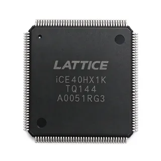
封装 144-pin TQFP
Package Family TQFP-144 LQFP surface-mount package
安装类型 Surface mount
FPGA Technology 90 nm
Programming Interface JTAG

LFE2-12E-5T144I tqfp-144 lqfp surface-mount package 引脚配置指南

LFE2-12E-5T144I(tqfp-144 lqfp surface-mount package 封装)的引脚配置。 该数字 IC 包含 GPIO、通信接口(UART、SPI、I2C)和电源引脚。请参阅制造商数据手册以了解复用引脚功能和配置选项。对嵌入式系统设计和 PCB 布局至关重要。

LFE2-12E-5T144I 的 tqfp-144 lqfp surface-mount package 封装引脚图

暂无详细引脚数据: LFE2-12E-5T144I.

请参阅 数据手册 以查看完整引脚配置。

典型应用

LFE2-12E-5T144I 适用于 6 应用s: Industrial Automation Controllers, RS-485 and RS-232 Protocol Bridges, Multichannel Measurement and Data Acquisition, Audio and Waveform Processing, Embedded Communications Equipment, Compact Control and Security Modules.

🏭

Industrial Automation Controllers

The LFE2-12E-5T144I suits compact industrial controllers that combine parallel machine I/O with deterministic timing and industrial-temperature requirements. Its 12K LUTs can host state machines, interlocks, counters, communication framing, and motion-control logic, while 93 I/O reduce the need for external glue logic. The 1.2 V core supports modern low-voltage FPGA architectures without requiring a separate processor for every control function. Use the manufacturer pinout to map field-bus and sensor signals to compatible I/O banks, and validate timing against the -5 speed grade before closing the system clocking plan.

🌐

RS-485 and RS-232 Protocol Bridges

The LFE2-12E-5T144I can implement protocol conversion, command parsing, checksum generation, and buffering between serial interfaces. Its 12K LUTs and one DSP block provide more logic capacity than a basic programmable logic device, allowing multiple channels and a supervisory state machine to share one FPGA. The 144-pin TQFP package offers 93 I/O for parallel host connections, status signals, and external memory. Validate voltage levels on each serial channel and keep transceiver direction control deterministic to prevent bus contention.

🧩

Multichannel Measurement and Data Acquisition

The LFE2-12E-5T144I is appropriate for sensor-acquisition systems that require parallel ADC control, digital filtering, calibration tables, and data packing. Its 12K LUTs can coordinate multiple converters, while the DSP block can accelerate multiply-accumulate operations used in filtering and scaling. The 93 I/O provide ample connections for converter clocks, data buses, control lines, status indicators, and external nonvolatile memory. Establish analog and digital partitioning carefully so switching converters and high-speed ADC clocks do not disturb sensitive measurement circuitry.

🎧

Audio and Waveform Processing

The LFE2-12E-5T144I can perform digital filtering, sample-rate conversion assistance, waveform generation, and interface bridging in audio equipment. Its DSP block is useful for multiply-accumulate filtering, while the remaining LUT capacity supports control, clock division, and buffer management. The 144-pin TQFP package gives a compact implementation with 93 I/O for codec signals and control lines. Clock the FPGA from a low-jitter source when signal quality depends on a stable sampling reference, and keep the codec interface within the voltage and timing limits of the selected bank.

🌐

Embedded Communications Equipment

The LFE2-12E-5T144I is useful in network-interface, protocol-conversion, and embedded communications modules where parallel data must be transformed into serial traffic. The FPGA can maintain packet framing, flow control, error checking, and timing relationships while external transceivers handle the physical layer. Its 12K LUTs allow control logic to coexist with the data path, and 93 I/O support external memory and parallel host buses. Confirm all interface voltage standards, implement clock-domain crossings conservatively, and validate signal integrity on high-speed links before environmental testing.

🔒

Compact Control and Security Modules

The LFE2-12E-5T144I can implement authentication routines, key-locking logic, command filters, or access-control functions in a compact programmable module. The one DSP block supports finite-state-machine processing and selected arithmetic operations, while 12K LUTs provide room for peripheral bridges and status logic. The 144-pin TQFP package supports compact board construction without sacrificing I/O availability. For security-critical equipment, add external tamper controls and protected key storage, and verify the FPGA configuration path against the system threat model.

What are the key specifications of LFE2-12E-5T144I that engineers should know?
The LFE2-12E-5T144I is a 12K-LUT ECP2 FPGA with 93 I/O, one DSP block, a 1.2 V core, and a 144-pin TQFP package. According to the Lattice Semiconductor manufacturer datasheet, the device uses 90 nm FPGA technology and is ordered in the -5 speed grade with an industrial-temperature designation. These figures place it in the ECP2 family and distinguish it from speed-, package-, and temperature-specific ordering options.
Where can I download the LFE2-12E-5T144I datasheet PDF?
The LFE2-12E-5T144I datasheet and supporting documentation are accessed through the Lattice Semiconductor product documentation and the product listing linked from this page. The manufacturer datasheet is the controlling reference for pin assignments, electrical limits, configuration requirements, AC timing, and package drawings. Confirm that the document applies specifically to the 12E device density, -5 speed grade, 144-pin package, and industrial-temperature suffix.
Where is the LFE2-12E-5T144I pinout located?
The LFE2-12E-5T144I pinout is in the package pin-description table and package drawing in the Lattice Semiconductor manufacturer datasheet. The device uses a 144-pin TQFP package, so all 144 positions must be checked before assigning power, ground, configuration, clock, JTAG, and user I/O functions. Use the manufacturer ordering information to confirm the exact package variant and do not infer pin functions from a similarly named device.
What is the difference between LFE2-12E-5T144I and LFE2-12E-6T144I?
The principal documented difference is speed grade: LFE2-12E-5T144I uses the -5 grade, while LFE2-12E-6T144I uses the -6 grade. Both retain the ECP2 12E device density and 144-pin TQFP organization shown by the product family data. The faster -6 option may better satisfy designs with more demanding timing paths, but the manufacturer timing tables and complete device comparison should be checked before interchangeability is assumed.
Is LFE2-12E-5T144I suitable for industrial control applications?
Yes, LFE2-12E-5T144I is appropriate for industrial control designs because its ordering code identifies the industrial-temperature option. The device provides 12K LUTs, 93 I/O, one DSP block, and a 1.2 V core for coordinating control logic and communication interfaces. Final suitability depends on the required ambient range, timing margin, isolation strategy, environmental qualification, and availability of a manufacturer configuration for the target board.
What can replace LFE2-12E-5T144I without changing the PCB footprint?
The closest same-package family candidates include LFE2-12E-5TN144I, LFE2-12E-6T144I, LFE2-12SE-5T144I, and LFE2-12SE-7TN144C, all associated with the 144-pin ECP2 package family. Compatibility must be checked for voltage, speed, temperature, configuration, and named-pin behavior before substitution. LFE2-12E-5Q208C and LFE2-12E-5F484I are excluded because their package pin counts differ from 144.
Is LFE2-12E-5T144I the same as LFE2-12E-5TN144I?
No, the two ordering codes should not be treated as automatically identical. LFE2-12E-5T144I is the industrial-temperature ordering option with a -5 speed grade, while LFE2-12E-5TN144I adds the N ordering character and has a distinct packaging or ordering designation. Both use the ECP2 12E family and 144-pin TQFP organization, but the manufacturer ordering table must be checked for exact grade, temperature, and packing differences.
When should I choose LFE2-12E-5T144I over LFE2-12E-6T144I?
Choose LFE2-12E-5T144I when its -5 timing grade satisfies the design and the industrial-temperature ordering option is required. Choose LFE2-12E-6T144I when the target logic needs the higher -6 performance grade or tighter timing margin. Both use the same ECP2 12E density and 144-pin TQFP family, so performance requirements and operating conditions—not footprint preference—should determine the selection.
Is LFE2-12E-5T144I the same as LFE2-12SE-5T144I?
The LFE2-12E-5T144I and LFE2-12SE-5T144I are related ECP2 devices in the same 144-pin package family, but the SE designation indicates a different configuration within the family. According to the manufacturer comparison terminology, the options can differ in package, speed, and temperature ratings, and family membership alone does not establish interchangeability. Compare device features and named pins before treating either part as a drop-in replacement.
How do I request a quote and lead time for LFE2-12E-5T144I?
Use the Request a Quote form on this page to request LFE2-12E-5T144I pricing, current lead time, stock status, and order quantity. The quote team can confirm the exact 144-pin package and ordering code before accepting an order. For production planning, provide the required annual volume, forecast cadence, programming needs, and delivery destination so the response reflects the intended build schedule.
Is LFE2-12E-5T144I in stock online?
Current LFE2-12E-5T144I stock status should be confirmed through the Request a Quote form on this page rather than inferred from a catalog listing. Include the required quantity and target delivery date in the request. For scheduled production, provide a rolling forecast and consignment requirements so the supplier can evaluate availability and the most appropriate allocation plan.
What is the price of LFE2-12E-5T144I?
The current LFE2-12E-5T144I price depends on order quantity, programmed or unprogrammed delivery condition, packaging, and supply status. Submit the required part quantity through the Request a Quote form on this page to receive current commercial terms. Providing a forecast and target ship date helps obtain a quotation that reflects the intended production schedule.
How much power does the LFE2-12E-5T144I use?
The LFE2-12E-5T144I operates from a 1.2 V core, but total board power depends on core activity, I/O loading, configuration state, and the selected I/O standards. The manufacturer datasheet provides the authoritative static and dynamic power information for design estimation. Account separately for external memory, transceiver, clock, and interface power because those rails can dominate the complete system consumption.
Does LFE2-12E-5T144I support DSP and signal-processing designs?
Yes, LFE2-12E-5T144I includes DSP resources and has 12K LUTs for surrounding control and data-path logic. The integrated DSP capability can accelerate multiplication, filtering, correlation, modulation, and related arithmetic operations without requiring a separate processor for every function. Final throughput depends on the selected clock, resource allocation, pipeline structure, memory interface, and timing closure of the complete design.
What design constraints matter for a 144-pin LFE2-12E-5T144I PCB?
The LFE2-12E-5T144I requires a 144-pin TQFP land pattern, careful power-plane distribution, local decoupling, and controlled routing for clocks and external memories. Use the manufacturer package drawing for mechanical dimensions and land pattern. Keep sensitive configuration and programming nets away from noisy sources, follow the recommended JTAG topology, and validate all I/O voltage standards against the selected bank power requirements.

工程参考数据: LFE2-12E-5T144I ——对比、设计指导和合规信息。

选型指南

Choose LFE2-12E-5T144I when the design needs 12K LUTs, 93 I/O, one DSP block, a 1.2 V core, and an industrial-temperature ECP2 device in a 144-pin TQFP package. Select LFE2-12E-6T144I if timing closure requires the faster -6 grade while preserving the same footprint and device density. Consider LFE2-12E-5TN144I when its exact ordering and packing designation meet the production plan. LFE2-12SE-5T144I and LFE2-12SE-7TN144C are candidates only after checking SE-specific configuration, speed, temperature, and named-pin requirements. Exclude LFE2-12E-5Q208C and LFE2-12E-5F484I when the existing board uses a 144-pin footprint. For every substitution, compare the manufacturer pinout, timing tables, configuration scheme, I/O standards, and qualification requirements before releasing a PCB or production order.

与替代料对比

参数 本产品 LFE2-12E-5TN144I LFE2-12E-6T144I LFE2-12SE-5T144I LFE2-12SE-7TN144C LFE2-12E-6TN144I
Package 144-pin TQFP 144-pin TQFP 144-pin TQFP 144-pin TQFP 144-pin TQFP 144-pin TQFP
Brand Lattice Semiconductor Lattice Semiconductor Lattice Semiconductor Lattice Semiconductor Lattice Semiconductor Lattice Semiconductor
Device Family ECP2 ECP2 ECP2 ECP2 ECP2 ECP2
Core Voltage 1.2 V 1.2 V 1.2 V 1.2 V 1.2 V 1.2 V
Speed Grade -5 -5 -6 -5 -7 -6
FPGA Technology 90 nm 90 nm 90 nm 90 nm 90 nm 90 nm

关键差异点

  • Industrial-temperature ordering option (对比 LFE2-12SE-7TN144C)
  • Higher speed option available in the same footprint (对比 LFE2-12E-5T144I)
  • Standard 12E configuration with one DSP block (对比 LFE2-12SE-5T144I)

设计说明

Use the manufacturer 144-pin TQFP land pattern and verify pin-1 orientation against the PCB CAD library. TQFP leads are closely spaced, so enforce the fabricator's minimum width and clearance rules. Keep sensitive clock and configuration traces away from high-current switching paths, and provide continuous ground planes wherever the package footprint allows.

Separate the 1.2 V core supply from I/O supplies and place local high-frequency decoupling close to the corresponding power and ground pins. Check the manufacturer power-sequencing table before combining external transceivers and memory. Account for simultaneous I/O switching current because a design that is stable at static power may fail only during high-activity data transfers.

Route clocks as short and continuous as possible, provide a defined return path beneath each high-speed trace, and avoid stubs or unnecessary test pads. Use the -5 timing grade margins from the manufacturer timing tables for external memory and transceiver interfaces. If timing closure is difficult, evaluate LFE2-12E-6T144I with the same 144-pin footprint rather than changing the board layout.

Do not select a family member solely from the LUT count and package. Confirm the E versus SE configuration, speed grade, temperature suffix, packing suffix, supported I/O standards, and configuration requirements. The 144-pin package variants LFE2-12E-5Q208C and LFE2-12E-5F484I are not footprint-compatible because they use 208-pin and 484-pin packages.

合规信息

RoHS
Unknown
REACH
Unknown
AEC-Q100
Unknown
无铅
Unknown
无卤
Unknown
冲突矿物
Unknown

The industrial-temperature ordering option is identified by the I suffix, but no specific RoHS, REACH, AEC-Q100, lead-free, halogen-free, or conflict-minerals declaration is stated in the product information. Confirm environmental and automotive requirements with the manufacturer before qualification.
数据核验日期: 2026-11-03 ——数据由 XAIPART 元器件工程团队核验和整理

相关搜索

LFE2-12E-5T144I datasheet LFE2-12E-5T144I pinout LFE2-12E-5T144I datasheet pdf LFE2-12E-5T144I equivalent LFE2-12E-5T144I replacement LFE2-12E-5T144I cross reference LFE2-12E-5T144I footprint LFE2-12E-5T144I schematic LFE2-12E-5T144I price LFE2-12E-5T144I stock Lattice LFE2-12E-5T144I LFE2-12E-5T144I vs LFE2-12E-6T144I LFE2-12E-5T144I 12K LUT 93 I/O LFE2-12E-5T144I TQFP-144 LFE2-12E-5T144I industrial FPGA

相关元器件 & 术语

Lattice Semiconductor LFE2-12E-5T144I LFE2-12E-5TN144I LFE2-12E-6T144I LFE2-12SE-5T144I LFE2-12SE-7TN144C LFE2-12E-6TN144I ECP2 FPGA field-programmable gate array programmable logic device semiconductor 12K LUTs 93 I/O DSP block 1.2 V core -5 speed grade industrial temperature grade 90 nm FPGA technology TQFP-144 LQFP surface-mount package JTAG industrial control signal processing
快速报价
填写完整信息——我们的销售团队将在 24 小时内回复
料号 制造商 封装 QTY 目标价 小计
✓
报价已提交!

我们将在 24 小时内回复您的邮件

1
询价已提交
2
已收到报价
3
已下单
4
支付
5
已发货
6
已送达
查看询价详情