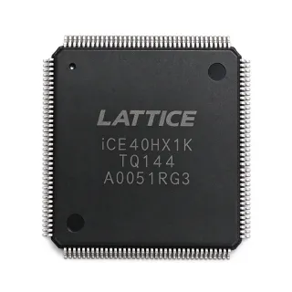
LFE2-12E-5T144I - 12K LUT ECP2 FPGA | Lattice Semiconductor
MPN: LFE2-12E-5T144I ✓ AktifLFE2-12E-5T144I Ringkasan
An FPGA is a configurable digital semiconductor whose interconnect and logic resources are programmed after manufacture. Within the product hierarchy, the LFE2-12E-5T144I is an FPGA, a programmable-logic device, and a semiconductor. Its configurable architecture allows parallel interfaces, control logic, signal conditioning, protocol handling, and data-processing functions to be consolidated into one device instead of using multiple fixed-function integrated circuits.
The principal device figures are 12K LUTs, 93 I/O, and a 144-pin TQFP package. The -5 ordering code identifies the performance grade, while the I suffix identifies the industrial temperature option. A 1.2 V core supports low-voltage digital operation, and the device includes DSP resources for designs requiring dedicated multiplication, filtering, waveform generation, or other arithmetic processing.
The ECP2 architecture supports implementation flexibility for control systems, communication interfaces, sensor acquisition, and general-purpose embedded logic. Its 93 I/O provide substantial board-level connectivity in a 144-pin package, reducing the need for external interface logic when pin resources and speed requirements fit the target design. Configuration storage, clocking, JTAG programming, and operating limits should be verified against the Lattice manufacturer documentation for the selected board and system configuration.
Typical uses include industrial automation controllers, RS-485 and RS-232 protocol bridges, multichannel measurement systems, audio and waveform processors, embedded communications equipment, and compact control modules. The FPGA is especially useful when several parallel data paths must be coordinated deterministically or when a product family must adapt to changing interface requirements through programmable logic.
PCB implementation requires strict attention to the 144-pin TQFP footprint, power and ground distribution, decoupling, clock routing, and high-speed signal integrity. Confirm pin assignments, configuration pins, supported clock sources, and interface voltage levels in the manufacturer pinout table before schematic capture. Programming should also include the correct bitstream and suitable JTAG configuration path for the assembled board.
This product summary consolidates the core device identity, ordered speed and temperature options, package details, application guidance, and compatible family alternatives into one engineering-focused reference for FPGA design and component sourcing.
Pilihan pengganti yang segera untuk LFE2-12E-5T144I — sama paket, pin-pin kompatibel. Bahagian paket yang berbeza memerlukan kerja ulang PCB diasingkan.
Varietas dalam siri ini
Model serupa yang kompatibel dengan pengganti yang segera LFE2-12E-5T144I (sama faktor bentuk dan kaki) — berbeza dalam Package, Speed Grade.
LFE2-12E-5TN144I
✅ Masuk Drop-In📋 Alternatif rujukan (tidak dalam katalog)
LFE2-12E-6T144I
✅ Masuk Drop-InHubungi untuk harga
Lihat Datasheet →LFE2-12SE-5T144I
✅ Masuk Drop-In📋 Alternatif rujukan (tidak dalam katalog)
LFE2-12SE-7TN144C
✅ Masuk Drop-In📋 Alternatif rujukan (tidak dalam katalog)
LFE2-12E-6TN144I
✅ Masuk Drop-In ⚠️ Spesifikasi Tidak Disahkan📋 Alternatif rujukan (tidak dalam katalog)
LFE2-12E-5T144I Penilaian maksimum & Ciri-ciri Elektrik
| Device Type | ECP2 field-programmable gate array (FPGA) |
| Logic Capacity | 12K LUTs |
| Equivalent Logic Cells | 12,000 cells |
| User I/O Count | 93 I/O |
| DSP Resources | 1 DSP block |
| Core Supply Voltage | 1.2 V |
| Speed Grade | -5 |
| Temperature Grade | Industrial |
| Kemasan | 144-pin TQFP |
| Package Family | TQFP-144 LQFP surface-mount package |
| Jenis Pemasangan | Surface mount |
| FPGA Technology | 90 nm |
| Programming Interface | JTAG |
Panduan Konfigurasi Pin LFE2-12E-5T144I tqfp-144 lqfp surface-mount package
Konfigurasi pin untuk LFE2-12E-5T144I (tqfp-144 lqfp surface-mount package pakai). IC digital ini termasuk GPIO, antaramuka komunikasi (UART, SPI, I2C), dan pin kuasa. Rujuk dokumen pengeluar untuk fungsi pin alternatif dan opsi konfigurasi. Biasa digunakan dalam rancangan sistem ter嵌入式 dan PCB.
Tiada data garisan pin yang diperoleh untuk LFE2-12E-5T144I.
Rujuk kepada lembaran data untuk konfigurasi pin penuh.
Aplikasi Biasa
LFE2-12E-5T144I patut untuk 6 aplikasis: Industrial Automation Controllers, RS-485 and RS-232 Protocol Bridges, Multichannel Measurement and Data Acquisition, Audio and Waveform Processing, Embedded Communications Equipment, Compact Control and Security Modules.
Industrial Automation Controllers
The LFE2-12E-5T144I suits compact industrial controllers that combine parallel machine I/O with deterministic timing and industrial-temperature requirements. Its 12K LUTs can host state machines, interlocks, counters, communication framing, and motion-control logic, while 93 I/O reduce the need for external glue logic. The 1.2 V core supports modern low-voltage FPGA architectures without requiring a separate processor for every control function. Use the manufacturer pinout to map field-bus and sensor signals to compatible I/O banks, and validate timing against the -5 speed grade before closing the system clocking plan.
Disebarkan
RS-485 and RS-232 Protocol Bridges
The LFE2-12E-5T144I can implement protocol conversion, command parsing, checksum generation, and buffering between serial interfaces. Its 12K LUTs and one DSP block provide more logic capacity than a basic programmable logic device, allowing multiple channels and a supervisory state machine to share one FPGA. The 144-pin TQFP package offers 93 I/O for parallel host connections, status signals, and external memory. Validate voltage levels on each serial channel and keep transceiver direction control deterministic to prevent bus contention.
Disebarkan
Multichannel Measurement and Data Acquisition
The LFE2-12E-5T144I is appropriate for sensor-acquisition systems that require parallel ADC control, digital filtering, calibration tables, and data packing. Its 12K LUTs can coordinate multiple converters, while the DSP block can accelerate multiply-accumulate operations used in filtering and scaling. The 93 I/O provide ample connections for converter clocks, data buses, control lines, status indicators, and external nonvolatile memory. Establish analog and digital partitioning carefully so switching converters and high-speed ADC clocks do not disturb sensitive measurement circuitry.
Disebarkan
Audio and Waveform Processing
The LFE2-12E-5T144I can perform digital filtering, sample-rate conversion assistance, waveform generation, and interface bridging in audio equipment. Its DSP block is useful for multiply-accumulate filtering, while the remaining LUT capacity supports control, clock division, and buffer management. The 144-pin TQFP package gives a compact implementation with 93 I/O for codec signals and control lines. Clock the FPGA from a low-jitter source when signal quality depends on a stable sampling reference, and keep the codec interface within the voltage and timing limits of the selected bank.
Disebarkan
Embedded Communications Equipment
The LFE2-12E-5T144I is useful in network-interface, protocol-conversion, and embedded communications modules where parallel data must be transformed into serial traffic. The FPGA can maintain packet framing, flow control, error checking, and timing relationships while external transceivers handle the physical layer. Its 12K LUTs allow control logic to coexist with the data path, and 93 I/O support external memory and parallel host buses. Confirm all interface voltage standards, implement clock-domain crossings conservatively, and validate signal integrity on high-speed links before environmental testing.
Disebarkan
Compact Control and Security Modules
The LFE2-12E-5T144I can implement authentication routines, key-locking logic, command filters, or access-control functions in a compact programmable module. The one DSP block supports finite-state-machine processing and selected arithmetic operations, while 12K LUTs provide room for peripheral bridges and status logic. The 144-pin TQFP package supports compact board construction without sacrificing I/O availability. For security-critical equipment, add external tamper controls and protected key storage, and verify the FPGA configuration path against the system threat model.
Disebarkan
Ringkasan Produk Disebarkan
Data referensi kejuruteraan untuk LFE2-12E-5T144I — perbandingan, panduan rancangan, dan maklumat kesediaan
Panduan Pilihan
Perbandingan dengan Gantian
| Parametr | Produk Ini | LFE2-12E-5TN144I | LFE2-12E-6T144I | LFE2-12SE-5T144I | LFE2-12SE-7TN144C | LFE2-12E-6TN144I |
|---|---|---|---|---|---|---|
| Package | 144-pin TQFP | 144-pin TQFP | 144-pin TQFP | 144-pin TQFP | 144-pin TQFP | 144-pin TQFP |
| Brand | Lattice Semiconductor | Lattice Semiconductor | Lattice Semiconductor | Lattice Semiconductor | Lattice Semiconductor | Lattice Semiconductor |
| Device Family | ECP2 | ECP2 | ECP2 | ECP2 | ECP2 | ECP2 |
| Core Voltage | 1.2 V | 1.2 V | 1.2 V | 1.2 V | 1.2 V | 1.2 V |
| Speed Grade | -5 | -5 | -6 | -5 | -7 | -6 |
| FPGA Technology | 90 nm | 90 nm | 90 nm | 90 nm | 90 nm | 90 nm |
Penyeberangsung Jelas
- Industrial-temperature ordering option (vsLFE2-12SE-7TN144C)
- Higher speed option available in the same footprint (vsLFE2-12E-5T144I)
- Standard 12E configuration with one DSP block (vsLFE2-12SE-5T144I)
Catatan Desain
Use the manufacturer 144-pin TQFP land pattern and verify pin-1 orientation against the PCB CAD library. TQFP leads are closely spaced, so enforce the fabricator's minimum width and clearance rules. Keep sensitive clock and configuration traces away from high-current switching paths, and provide continuous ground planes wherever the package footprint allows.
Separate the 1.2 V core supply from I/O supplies and place local high-frequency decoupling close to the corresponding power and ground pins. Check the manufacturer power-sequencing table before combining external transceivers and memory. Account for simultaneous I/O switching current because a design that is stable at static power may fail only during high-activity data transfers.
Route clocks as short and continuous as possible, provide a defined return path beneath each high-speed trace, and avoid stubs or unnecessary test pads. Use the -5 timing grade margins from the manufacturer timing tables for external memory and transceiver interfaces. If timing closure is difficult, evaluate LFE2-12E-6T144I with the same 144-pin footprint rather than changing the board layout.
Do not select a family member solely from the LUT count and package. Confirm the E versus SE configuration, speed grade, temperature suffix, packing suffix, supported I/O standards, and configuration requirements. The 144-pin package variants LFE2-12E-5Q208C and LFE2-12E-5F484I are not footprint-compatible because they use 208-pin and 484-pin packages.
Maklumat Kesediaan
The industrial-temperature ordering option is identified by the I suffix, but no specific RoHS, REACH, AEC-Q100, lead-free, halogen-free, or conflict-minerals declaration is stated in the product information. Confirm environmental and automotive requirements with the manufacturer before qualification.