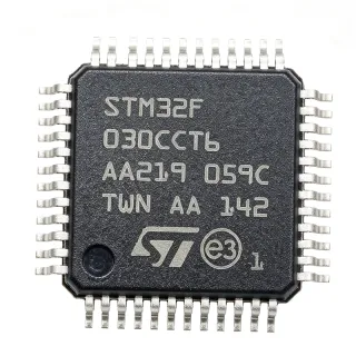
STM32F303CCT6 - 256KB Flash, 72MHz ARM Cortex-M4F MCU | STMicroelectronics
料号: STM32F303CCT6 ✓ 量产中| 数量 | 单价 | 小计 |
|---|---|---|
| 1 | $8.5 | $8.50 |
| 10 | $7.8 | $78.00 |
| 100 | $6.9 | $690.00 |
| 500 | $6.2 | $3,100.00 |
| 1,000 | $5.6 | $5,600.00 |
STM32F303CCT6 概述
A microcontroller (MCU) is a compact integrated circuit designed to govern a specific operation in an embedded system. It contains a processor core, memory, and programmable input/output peripherals. The STM32F303CCT6 belongs to the STM32F3 series, which is optimized for analog-intensive applications such as motor control, industrial sensors, and power management. The Cortex-M4F core adds a floating-point unit (FPU) and DSP instructions, enabling efficient handling of complex mathematical operations.
Key features include a 72 MHz ARM Cortex-M4F core with FPU, 256 KB Flash, 40 KB SRAM, and a rich set of analog peripherals: three 12-bit ADCs (up to 5 MSPS), four 12-bit DACs, seven fast comparators, and programmable gain amplifiers (PGA). It also integrates advanced timers (up to 8 timers), a real-time clock (RTC), and multiple communication interfaces including I2C, SPI, USART, CAN, and USB. The device supports a temperature range of -40°C to +85°C and is available in a 48-pin LQFP package.
The STM32F303CCT6 leverages ST's advanced 90nm process technology, providing a balance of performance and power efficiency. The Cortex-M4F core with FPU accelerates signal processing tasks, while the extensive analog peripherals reduce the need for external components. The device includes a memory protection unit (MPU), DMA controller, and a nested vectored interrupt controller (NVIC) for real-time responsiveness.
Typical applications include motor control (field-oriented control), industrial automation, medical devices, and consumer electronics. The high-resolution ADCs and fast comparators make it ideal for closed-loop control systems, while the CAN interface supports automotive and industrial networking. The USB interface enables connectivity for data logging and firmware updates.
When designing with this device, ensure proper decoupling of the VDD and VDDA pins with 100nF capacitors placed close to the pins. The VDDA pin must be connected to a clean analog supply to achieve the specified ADC performance. Use the internal voltage regulator with external capacitors as recommended in the datasheet to ensure stable operation.
直接替换替代料: STM32F303CCT6 ——相同封装,引脚兼容。需要 PCB 改动的不同封装料号已排除。
本系列中的变体
可与以下型号直接替换的同系列型号: STM32F303CCT6 (相同外形与封装尺寸) ——差异在于 Core, Timers, Package, SRAM, Comparators.
快速对比工具——选择替代料号进行并排对比:
STM32F303CBT6
✅ 直接替换 ⚠️ 规格未核验✓ 有现货
$4.16 / 个
查看数据手册 →STM32F303CCT7
✅ 直接替换 ⚠️ 规格未核验📋 参考替代料(不在目录中)
STM32F303C8T6
✅ 直接替换 ⚠️ 规格未核验📋 参考替代料(不在目录中)
STM32F303CCT6 最大额定值与电气特性
| Core | ARM Cortex-M4F with FPU |
| 最大时钟频率 | 72 MHz |
| Flash Memory | 256 KB |
| SRAM | 40 KB |
| Supply Voltage Range | 2.0 V to 3.6 V |
| 封装 | LQFP-48 (7x7 mm) |
| 工作温度范围 | -40C to +85C |
| Number of I/O Pins | 37 |
| ADC Resolution | 12-bit |
| Number of ADCs | 3 |
| DAC Resolution | 12-bit |
| Number of DACs | 2 |
| Communication Interfaces | I2C, SPI, USART, CAN, USB |
| Timers | 8 (including advanced timers) |
| DMA Channels | 12 |
| RoHS 状态 | Compliant |
STM32F303CCT6 引脚配置
| 引脚 1 | VBAT — Battery backup supply for RTC |
| 引脚 2 | PC13 — GPIO / RTC tamper |
| 引脚 3 | PC14 — GPIO / OSC32_IN |
| 引脚 4 | PC15 — GPIO / OSC32_OUT |
| 引脚 5 | PF0 — GPIO / OSC_IN |
| 引脚 6 | PF1 — GPIO / OSC_OUT |
| 引脚 7 | NRST — Reset (active low) |
| 引脚 8 | VSSA — Analog ground |
| 引脚 9 | VDDA — Analog power supply |
| 引脚 10 | PA0 — GPIO / ADC / DAC / TIM2_CH1 |
| 引脚 11 | PA1 — GPIO / ADC / DAC / TIM2_CH2 |
| 引脚 12 | PA2 — GPIO / ADC / USART2_TX / TIM2_CH3 |
| 引脚 13 | PA3 — GPIO / ADC / USART2_RX / TIM2_CH4 |
| 引脚 14 | PA4 — GPIO / ADC / SPI1_NSS / DAC_OUT1 |
| 引脚 15 | PA5 — GPIO / ADC / SPI1_SCK / DAC_OUT2 |
| 引脚 16 | PA6 — GPIO / ADC / SPI1_MISO / TIM3_CH1 |
| 引脚 17 | PA7 — GPIO / ADC / SPI1_MOSI / TIM3_CH2 |
| 引脚 18 | PB0 — GPIO / ADC / TIM3_CH3 |
| 引脚 19 | PB1 — GPIO / ADC / TIM3_CH4 |
| 引脚 20 | PB2 — GPIO / BOOT1 |
| 引脚 21 | PB10 — GPIO / I2C2_SCL / USART3_TX |
| 引脚 22 | PB11 — GPIO / I2C2_SDA / USART3_RX |
| 引脚 23 | VSS — Ground |
| 引脚 24 | VDD — Power supply |
| 引脚 25 | PB12 — GPIO / SPI2_NSS / I2S2_WS |
| 引脚 26 | PB13 — GPIO / SPI2_SCK / I2S2_CK |
| 引脚 27 | PB14 — GPIO / SPI2_MISO / I2S2_MCK |
| 引脚 28 | PB15 — GPIO / SPI2_MOSI / I2S2_SD |
| 引脚 29 | PA8 — GPIO / MCO / TIM1_CH1 |
| 引脚 30 | PA9 — GPIO / USART1_TX / TIM1_CH2 |
| 引脚 31 | PA10 — GPIO / USART1_RX / TIM1_CH3 |
| 引脚 32 | PA11 — GPIO / USB_DM / CAN_RX |
| 引脚 33 | PA12 — GPIO / USB_DP / CAN_TX |
| 引脚 34 | PA13 — GPIO / SWDIO |
| 引脚 35 | VSS — Ground |
| 引脚 36 | VDD — Power supply |
| 引脚 37 | PA14 — GPIO / SWCLK |
| 引脚 38 | PA15 — GPIO / JTDI / TIM2_CH1 |
| 引脚 39 | PB3 — GPIO / JTDO / TIM2_CH2 |
| 引脚 40 | PB4 — GPIO / NJTRST / TIM3_CH1 |
| 引脚 41 | PB5 — GPIO / I2C1_SMBA / TIM3_CH2 |
| 引脚 42 | PB6 — GPIO / I2C1_SCL / TIM4_CH1 |
| 引脚 43 | PB7 — GPIO / I2C1_SDA / TIM4_CH2 |
| 引脚 44 | BOOT0 — Boot mode selection |
| 引脚 45 | PB8 — GPIO / CAN_RX / TIM4_CH3 |
| 引脚 46 | PB9 — GPIO / CAN_TX / TIM4_CH4 |
| 引脚 47 | VSS — Ground |
| 引脚 48 | VDD — Power supply |
典型应用
STM32F303CCT6 适用于 6 应用s: Motor Control, Industrial Automation, Medical Devices, Consumer Electronics, Power Management, IoT and Smart Home.
Motor Control
The STM32F303CCT6 is ideal for motor control applications, particularly field-oriented control (FOC) of brushless DC (BLDC) motors. Its advanced timers generate complementary PWM signals with dead-time insertion, while the high-speed ADCs (up to 5 MSPS) sample phase currents with minimal delay. The Cortex-M4F FPU accelerates the Clarke and Park transforms required for FOC, enabling efficient and smooth motor operation. The fast comparators provide overcurrent protection, and the CAN interface allows integration into industrial networks. With a 72 MHz core and 256 KB Flash, complex control algorithms can be implemented without external DSPs.
推荐
Industrial Automation
In industrial automation, the STM32F303CCT6 serves as a central controller for PLCs, sensors, and actuators. Its multiple communication interfaces (USART, SPI, I2C, CAN) enable seamless connectivity to fieldbus networks and peripheral devices. The 12-bit ADCs with up to 5 MSPS sampling rate allow precise measurement of analog signals from sensors, while the DACs can generate analog control signals. The device's robust operating temperature range (-40°C to +85°C) and low-power modes make it suitable for harsh industrial environments. The 256 KB Flash provides ample space for firmware updates and data logging.
推荐
Medical Devices
The STM32F303CCT6 is well-suited for medical devices such as patient monitors, infusion pumps, and diagnostic equipment. Its high-resolution ADCs and DACs enable accurate signal acquisition and generation, critical for biomedical signal processing. The FPU accelerates algorithms like digital filtering and ECG analysis. The device's low-power modes extend battery life in portable medical devices. The USB interface allows connectivity to PCs for data transfer and firmware updates. The wide supply voltage range (2.0V to 3.6V) accommodates various battery chemistries. ST's commitment to quality and long-term availability makes it a reliable choice for medical applications.
推荐
Consumer Electronics
In consumer electronics, the STM32F303CCT6 can be used in smart home devices, wearables, and audio equipment. Its rich peripheral set includes USB, I2S (via SPI), and multiple timers, enabling audio playback, sensor interfacing, and user interface control. The FPU supports audio processing algorithms like equalization and noise reduction. The device's small LQFP-48 package is suitable for compact designs. Low-power modes are essential for battery-powered devices, and the device can wake from Stop mode via external interrupts. The 256 KB Flash allows for feature-rich firmware, and the CAN interface can be used for home automation networks.
推荐
Power Management
The STM32F303CCT6 is used in power management systems for digital power conversion, battery management, and UPS control. Its fast ADCs and comparators enable precise voltage and current monitoring, while the advanced timers generate PWM signals for DC-DC converters. The FPU accelerates control loop calculations, improving efficiency and transient response. The device's multiple communication interfaces allow monitoring and configuration via I2C or CAN. The wide supply voltage range and low-power modes are beneficial for energy-efficient designs. The 256 KB Flash supports complex state machines and fault handling routines.
推荐
IoT and Smart Home
The STM32F303CCT6 is a strong candidate for IoT edge nodes and smart home hubs. Its low-power modes (Stop, Standby) enable battery-powered operation for years. The device supports various wireless modules via SPI or UART, such as Wi-Fi, BLE, and LoRa. The FPU and DSP instructions allow on-device processing of sensor data, reducing cloud dependency. The USB interface can be used for configuration and firmware updates. The CAN interface is useful for wired smart home networks. With 256 KB Flash, developers can implement robust security features like encryption and secure boot. The device's wide temperature range makes it suitable for outdoor sensors.
推荐
推荐产品汇总
工程参考数据: STM32F303CCT6 ——对比、设计指导和合规信息。
选型指南
与替代料对比
| 参数 | 本产品 | STM32F303CBT6 | STM32F303CCT7 | STM32F303C8T6 | STM32F303RCT6 |
|---|---|---|---|---|---|
| Package | LQFP-48 | LQFP-48 | LQFP-48 | LQFP-48 | LQFP-64 |
| Brand | STMicroelectronics | STMicroelectronics | STMicroelectronics | STMicroelectronics | STMicroelectronics |
| Core | ARM Cortex-M4F | ARM Cortex-M4F | ARM Cortex-M4F | ARM Cortex-M4F | ARM Cortex-M4F |
| Max Clock Frequency | 72 MHz | 72 MHz | 72 MHz | 72 MHz | 72 MHz |
| Flash Memory | 256 KB | 128 KB | 256 KB | 64 KB | 256 KB |
| SRAM | 40 KB | 32 KB | 40 KB | 16 KB | 40 KB |
| Number of I/O Pins | 37 | 37 | 37 | 37 | 51 |
| Operating Temperature Range | -40C to +85C | -40C to +85C | -40C to +105C | -40C to +85C | -40C to +85C |
关键差异点
- Higher Flash memory (256 KB) compared to STM32F303CBT6 (对比 STM32F303CBT6)
- Extended temperature range option (STM32F303CCT7) (对比 STM32F303CCT7)
- More SRAM (40 KB) than STM32F303C8T6 (对比 STM32F303C8T6)
设计说明
Ensure proper decoupling of VDD and VDDA pins. Place a 100nF ceramic capacitor as close as possible to each VDD pin, and a 1uF capacitor on VDDA. The VDDA pin must be connected to a clean analog supply to achieve the specified ADC performance. Use a ferrite bead between VDD and VDDA if the digital supply is noisy.
For the LQFP-48 package, use a 4-layer PCB with a solid ground plane. Route the crystal oscillator (OSC_IN/OSC_OUT) with short traces and keep them away from high-speed digital signals. Place the boot configuration resistors (BOOT0) with proper pull-up/pull-down to avoid unintended boot modes. Follow ST's layout guidelines in AN4666 for best EMC performance.
Do not leave unused I/O pins floating; configure them as outputs or enable internal pull-ups/pull-downs to reduce power consumption and avoid noise. Ensure the NRST pin has a 100nF capacitor to ground for reliable reset. When using the ADC, avoid switching digital I/O during conversion to prevent noise coupling. Also, verify that the supply voltage does not exceed 3.6V to prevent damage.
合规信息
RoHS compliant per STMicroelectronics. Not AEC-Q100 qualified; for automotive use, consider STM32F303CCT7 which has extended temperature range but still not AEC-Q100.