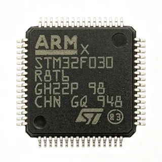
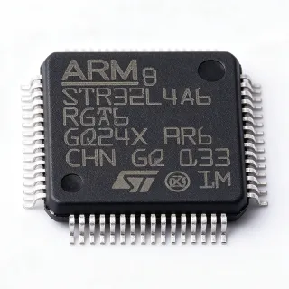
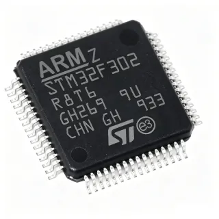
STM32F405RGT6TR - 168MHz Cortex-M4F MCU 1MB Flash | STMicroelectronics
料号: STM32F405RGT6TR ✓ 量产中| 数量 | 单价 | 小计 |
|---|---|---|
| 1 | $12.45 | $12.45 |
| 10 | $11.18 | $111.80 |
| 100 | $9.85 | $985.00 |
| 500 | $8.92 | $4,460.00 |
| 1,000 | $7.65 | $7,650.00 |
STM32F405RGT6TR 概述
A microcontroller (MCU) is a single-chip computer that integrates a CPU core, program memory (Flash), data memory (SRAM), and a rich set of peripherals into one package. The Cortex-M4F class sits in the middle of the ARM microcontroller hierarchy (Cortex-M0/M0+ -> M3 -> M4F -> M7), gaining a single-precision floating-point unit and full DSP instruction set while retaining deterministic interrupt response and ultra-low-power modes. The STM32F405xx family is therefore aimed at applications that need high-throughput signal processing and connectivity without sacrificing real-time determinism, sitting between Cortex-M3 general-purpose MCUs and Cortex-M7 high-end parts in ST's STM32 family tree.
Key features of the STM32F405RGT6TR include an Adaptive Real-Time (ART) accelerator that allows 0-wait-state execution from Flash memory, a memory protection unit (MPU), 17 timers, three 12-bit ADCs (up to 2.4 MSPS), two 12-bit DACs, USB OTG Full-Speed and High-Speed, an internal Ethernet MAC with hardware IEEE 1588v2 support, a CAN 2.0B interface, SDIO, FSMC, and a CMOS-camera interface. DSP instructions and the single-precision FPU allow efficient audio, motor-control, and signal-chain math at clock speeds well above most Cortex-M3 competitors.
The architecture combines a 3-stage pipeline Cortex-M4F core with a multi-AHB bus matrix and an ART accelerator prefetch buffer, eliminating the Flash wait-state penalty that historically bottlenecked MCU throughput. The integrated PHY on selected packages and the hardware cryptography-ready subsystem (F405 variant) make this part suitable for industrial Ethernet and networked sensor nodes where determinism and bandwidth coexist.
Typical applications include industrial motor drives (FOC for 3-phase PMSM/BLDC), UAV flight controllers and quadcopters, audio processing and effects units, multi-axis robotics controllers, USB peripherals and HID devices, and Ethernet-connected IoT gateways. The 168 MHz core plus FPU makes real-time DSP tasks such as FFT, Kalman filtering, and audio sample-rate conversion straightforward without offloading to a companion DSP.
When designing with this part, allocate at least 4 decoupling capacitors (100 nF + 4.7 µF) within 5 mm of the VDD/VBAT/VDDA pins, keep the HSE crystal traces short and symmetric, and provide a solid ground pour under the LQFP-64 thermal pad to keep theta_JA within datasheet limits.
This page synthesizes distributor pricing, drop-in same-package alternatives (including GD32F405RGT6 and STM32F415RGT6), and practical design notes not found in the manufacturer datasheet alone.
直接替换替代料: STM32F405RGT6TR ——相同封装,引脚兼容。需要 PCB 改动的不同封装料号已排除。
本系列中的变体
可与以下型号直接替换的同系列型号: STM32F405RGT6TR (相同外形与封装尺寸) ——差异在于 Communication Interfaces, Package, SRAM, Flash Memory, Camera Interface.
快速对比工具——选择替代料号进行并排对比:
STM32F415RGT6
✅ 直接替换✓ 有现货
$8.1 / 个
查看数据手册 →STM32F407RGT6
✅ 直接替换📋 参考替代料(不在目录中)
STM32F407VGT6TR
✅ 直接替换✓ 有现货
$7.55 / 个
查看数据手册 →GD32F405RGT6
✅ 直接替换📋 参考替代料(不在目录中)
GD32F407RGT6
✅ 直接替换📋 参考替代料(不在目录中)
STM32F405RGT6TR 最大额定值与电气特性
| Core Architecture | ARM Cortex-M4F with single-precision FPU and DSP instructions |
| Maximum CPU Clock | 168 MHz |
| DMIPS Performance | 210 DMIPS / 1.25 DMIPS/MHz (Dhrystone 2.1) |
| Flash Memory | 1 MB |
| SRAM | 192 KB main + 4 KB backup |
| 封装 | LQFP-64 (10x10 mm) |
| Supply Voltage Range | 1.8 V to 3.6 V |
| 工作温度 | -40 C to +85 C |
| ADCs | 3x 12-bit, up to 2.4 MSPS |
| DACs | 2x 12-bit |
| Timers | 17 (including 2x 32-bit) |
| Communication Interfaces | USB OTG FS + HS, Ethernet MAC (IEEE 1588v2), 2x CAN 2.0B, 3x SPI, 3x I2C, 6x USART/UART, SDIO, FSMC |
| ART Accelerator | Yes - 0-wait-state Flash execution |
| Camera Interface | 8/10/12-bit CMOS sensor IF (STM32F407 series extended) |
| 安装类型 | Surface Mount |
| MSL 等级 | 3 (168 hours) |
| RoHS 状态 | Compliant |
STM32F405RGT6TR 引脚配置
| 引脚 1 | VBAT — RTC battery supply |
| 引脚 2 | PC13 — GPIO; Tamper-RTC (PC13) |
| 引脚 3 | PC14/OSC32_IN — LSE oscillator pin or GPIO |
| 引脚 4 | PC15/OSC32_OUT — LSE oscillator pin or GPIO |
| 引脚 5 | OSC_IN — HSE oscillator in |
| 引脚 6 | OSC_OUT — HSE oscillator out |
| 引脚 7 | NRST — Reset (active low) |
| 引脚 8 | VSSA — Analog ground |
| 引脚 9 | VDDA — Analog supply |
| 引脚 10 | PA0-WKUP — GPIO; ADC1/2 IN0; WKUP |
| 引脚 11 | PA1 — GPIO; ADC1/2 IN1 |
| 引脚 12 | PA2 — GPIO; ADC1/2 IN2; USART2_TX |
| 引脚 13 | PA3 — GPIO; ADC1/2 IN3; USART2_RX |
| 引脚 14 | PA4 — GPIO; ADC1/2 IN4; SPI1_NSS |
| 引脚 15 | PA5 — GPIO; ADC1/2 IN5; SPI1_SCK |
| 引脚 16 | PA6 — GPIO; ADC1/2 IN6; SPI1_MISO |
| 引脚 17 | PA7 — GPIO; ADC1/2 IN7; SPI1_MOSI |
| 引脚 18 | PB0 — GPIO; ADC1/2 IN8 |
| 引脚 19 | PB1 — GPIO; ADC1/2 IN9 |
| 引脚 20 | PB2/BOOT1 — GPIO; BOOT1 strap |
| 引脚 21 | PB10 — GPIO; I2C2_SCL; USART3_TX |
| 引脚 22 | PB11 — GPIO; I2C2_SDA; USART3_RX |
| 引脚 23 | VSS_1 — Digital ground |
| 引脚 24 | VDD_1 — Digital supply (1.8V-3.6V) |
| 引脚 25 | PB12 — GPIO; SPI2_NSS; CAN2_RX |
| 引脚 26 | PB13 — GPIO; SPI2_SCK; CAN2_TX |
| 引脚 27 | PB14 — GPIO; SPI2_MISO |
| 引脚 28 | PB15 — GPIO; SPI2_MOSI |
| 引脚 29 | PA8 — GPIO; USART1_CK; MCO1 |
| 引脚 30 | PA9 — GPIO; USART1_TX |
| 引脚 31 | PA10 — GPIO; USART1_RX |
| 引脚 32 | PA11 — GPIO; USB OTG FS DM |
| 引脚 33 | PA12 — GPIO; USB OTG FS DP |
| 引脚 34 | PA13 — GPIO; JTMS-SWDIO |
| 引脚 35 | VSS_2 — Digital ground |
| 引脚 36 | VDD_2 — Digital supply |
| 引脚 37 | PA14 — GPIO; JTCK-SWCLK |
| 引脚 38 | PA15 — GPIO; JTDI; SPI3_NSS |
| 引脚 39 | PB3 — GPIO; JTDO; SPI3_SCK |
| 引脚 40 | PB4 — GPIO; NJTRST; SPI3_MISO |
| 引脚 41 | PB5 — GPIO; I2C1_SMBAI |
| 引脚 42 | PB6 — GPIO; I2C1_SCL; USART1_TX |
| 引脚 43 | PB7 — GPIO; I2C1_SDA; USART1_RX |
| 引脚 44 | BOOT0 — Boot mode select (must be held at startup) |
| 引脚 45 | PB8 — GPIO; I2C1_SCL; CAN1_RX |
| 引脚 46 | PB9 — GPIO; I2C1_SDA; CAN1_TX |
| 引脚 47 | VSS_3 — Digital ground |
| 引脚 48 | VDD_3 — Digital supply |
| 引脚 49 | VSS_4 — Digital ground |
| 引脚 50 | VDD_4 — Digital supply |
| 引脚 51 | PE2 — GPIO; FSMC_A23 |
| 引脚 52 | PE3 — GPIO; FSMC_A19 |
| 引脚 53 | PE4 — GPIO; FSMC_A20 |
| 引脚 54 | PE5 — GPIO; FSMC_A21 |
| 引脚 55 | PE6 — GPIO; FSMC_A22 |
| 引脚 56 | VBAT — Battery domain supply (tied with pin 1) |
| 引脚 57 | PD0 — GPIO; FSMC_D2 |
| 引脚 58 | PD1 — GPIO; FSMC_D3 |
| 引脚 59 | VREF+ — ADC reference voltage positive |
| 引脚 60 | VREF- — ADC reference voltage negative |
| 引脚 61 | PA0_WKUP — GPIO; ADC IN0; WKUP (alternate ref) |
| 引脚 62 | PC0 — GPIO; ADC1/2 IN10 |
| 引脚 63 | PC1 — GPIO; ADC1/2 IN11 |
| 引脚 64 | VSS_5 — Digital ground |
典型应用
STM32F405RGT6TR 适用于 7 应用s: Drone Flight Controller / UAV FC, Industrial Motor Control / FOC Drive, USB Peripherals and Audio Interfaces, Ethernet-Connected IoT Gateway, Audio DSP and Effects Processors, Multi-Axis Robotics Controller, Medical Monitoring and Diagnostic Devices.
Drone Flight Controller / UAV FC
The STM32F405RGT6TR's 168 MHz Cortex-M4F core with single-precision FPU plus 1 MB Flash and 192 KB SRAM make it a benchmark flight-controller MCU for F4-class quadcopters and racing drones. The ART accelerator eliminates the Flash wait-state penalty at 168 MHz, so PID loops, gyro filtering (typically 8 kHz), and Betaflight/INAV firmware run with deterministic timing. Three 12-bit ADCs sample multi-axis gyro/accelerometer current-sensing channels concurrently, while the DMA controller offloads SPI/USB traffic without CPU intervention. Five UART channels and one I2C connect GPS, radio receivers, ESC telemetry, magnetometers, and I2C peripherals simultaneously. Compared with the STM32F722 (older F7-class), the F405 provides a stable, broadly supported firmware platform with abundant reference designs. PCB layout must keep the HSE crystal within 5 mm and provide a solid ground plane; pairing the MCU with an MPU6000 or ICM-42688 IMU over SPI is the canonical reference design.
推荐
Industrial Motor Control / FOC Drive
PMSM/BLDC motor drives benefit from the STM32F405RGT6TR's Cortex-M4F with FPU and DSP extensions at 168 MHz, 192 KB SRAM for control-loop buffers, and three 12-bit ADCs capable of 2.4 MSPS for current/voltage sampling. The CMSIS-DSP library accelerates Park/Clarke transforms and FIR filtering directly without offloading to a DSP; FOC commutates a 3-phase inverter at switching frequencies above 20 kHz while leaving headroom for housekeeping. The 1 MB Flash accommodates full ST Motor Control Workbench firmware and parameter tables; 2x CAN 2.0B ports support CANopen or CiA 402 communication with industrial inverters. For very high-FOC applications HRTIM-equipped STM32G474 or STM32F303 may be preferred, but the F405 is sufficient for general industrial drives under 1 kW. The exposed pad thermal management is straightforward thanks to the 10x10 mm LQFP-64 package, and reference designs in STM32-MC-KIT simplify qualification.
推荐
USB Peripherals and Audio Interfaces
The STM32F405RGT6TR integrates USB OTG High-Speed and Full-Speed controllers plus an I2S peripheral set, making it ideal for USB Audio Class 2.0 DAC/ADC interfaces, MIDI controllers, and HID peripherals. The Cortex-M4F at 168 MHz runs USB HS interrupt processing with ample headroom for 32-bit/384 kHz audio stream buffering through DMA, while the FPU accelerates biquad/mixing operations. 1 MB Flash stores USB class descriptors and full FX plugin libraries without compression, and 192 KB SRAM handles multi-channel audio buffers. Reference designs based on the STM32F4DISCOVERY board exist for USB-to-I2S bridges and ASIO-style interfaces; pairing the MCU with a PCM5102A DAC or PCM1808 ADC over I2S provides a proven audio pipeline. The package's 64-pin LQFP with USB D+/D- directly accessible simplifies layout; ESD protection on the USB pins remains essential.
推荐
Ethernet-Connected IoT Gateway
The STM32F405RGT6TR integrates a 10/100 Ethernet MAC with IEEE 1588v2 hardware timestamping, plus USB OTG HS, making it a strong choice for industrial IoT gateways, building-automation controllers, and Modbus TCP bridges. Combined with an external PHY (e.g., LAN8742A or DP83848), it forms a deterministic Ethernet node while running TCP/IP stacks such as lwIP or CycloneTCP on the Cortex-M4F. The 1 MB Flash holds full TLS stacks and OTA update handlers without external storage; 192 KB SRAM accommodates simultaneous TCP socket buffers for typical 4-8 concurrent connections. CAN 2.0B and USB OTG support a broad mix of field-bus to Ethernet bridging scenarios. JTAG over PA13/PA14/PA15/PB3 simplifies in-field firmware updates; the STM32 ecosystem includes X-CUBE-AWS/Azure plug-ins for direct cloud connectivity.
推荐
Audio DSP and Effects Processors
The Cortex-M4F with single-precision FPU and DSP extensions turns the STM32F405RGT6TR into a cost-effective audio effects engine for guitar pedals, studio FX, and karaoke processors. The FPU executes biquad, reverb, and pitch-shift algorithms at 168 MHz without integer-overflow artefacts, and CMSIS-DSP accelerates FFT and convolution. 1 MB Flash stores multiple effect banks plus dual-bank bootloader for safe OTA, while 192 KB SRAM is sufficient for several seconds of delay-line memory at 48 kHz mono. The I2S/SAI peripherals connect directly to audio CODECs (WM8960, AK4556); USB OTG FS enables a USB-MIDI device profile for studio integration. Compared with dedicated DSPs (e.g., ADAU1701), the F405 is cheaper, more programmable, and more accessible to hobbyists.
推荐
Multi-Axis Robotics Controller
Multi-axis robot controllers benefit from the STM32F405RGT6TR's combination of 168 MHz throughput, 17 timers, three 12-bit ADCs, and dual CAN 2.0B ports for servo/arm control. The 1 MB Flash hosts inverse-kinematics models, trajectory planners, and EtherCAT/CANopen slave stacks concurrently. DMA offloads encoder-counting from SPI to free CPU cycles for state-machine logic, while the FPU handles matrix-math for transformation between joint frames in real time. FSMC allows direct parallel connection to an FPGA-based motion-coprocessor if even higher throughput is required. With USB OTG, the board also serves as a USB host for end-effector tool swapping. The 64-pin LQFP provides enough GPIO for up to 6 incremental encoders plus step/direction generators.
推荐
Medical Monitoring and Diagnostic Devices
Battery-powered medical monitoring devices such as portable ECG, pulse oximeters, and SpO2 patient monitors rely on the STM32F405RGT6TR's FPU/DSP for in-line signal processing on-device. The Cortex-M4F at 168 MHz runs digital biquad filters, FFT-based heart-rate variability algorithms, and motion-artifact compensation; the FPU yields single-precision results that meet IEC 60601-2-25 algorithmic accuracy. 1 MB Flash stores persistent configuration and calibration tables; 192 KB SRAM holds multi-second waveform buffers at 500 Hz sampling. USB OTG enables direct PC connectivity for clinical software without external bridges. Low-power Run and Standby modes support battery life targets; the 4 KB backup SRAM and RTC allow uninterrupted timekeeping during sleep. Note that medical device compliance (IEC 60601-1) is a system-level consideration beyond the MCU selection alone.
推荐
推荐产品汇总
工程参考数据: STM32F405RGT6TR ——对比、设计指导和合规信息。
选型指南
与替代料对比
| 参数 | 本产品 | STM32F415RGT6 | STM32F407RGT6 | STM32F407VGT6TR | GD32F405RGT6 | GD32F407RGT6 |
|---|---|---|---|---|---|---|
| Brand | STMicroelectronics | STMicroelectronics | STMicroelectronics | STMicroelectronics | GigaDevice | GigaDevice |
| Package | LQFP-64 (10x10) | LQFP-64 (10x10) | LQFP-64 (10x10) | LQFP-64 (10x10) | LQFP-64 (10x10) | LQFP-64 (10x10) |
| Maximum CPU Clock | 168 MHz | 168 MHz | 168 MHz | 168 MHz | 168 MHz | 168 MHz |
| Flash Memory | 1 MB | 1 MB | 1 MB | 1 MB | 1 MB | 1 MB |
| SRAM | 192 KB + 4 KB | 192 KB + 4 KB | 192 KB + 4 KB | 192 KB + 4 KB | 192 KB + 4 KB | 192 KB + 4 KB |
| USB OTG | FS + HS | FS + HS | FS + HS | FS + HS | FS + HS | FS + HS |
| Ethernet MAC | Yes (IEEE 1588v2) | Yes (IEEE 1588v2) | Yes (IEEE 1588v2) | Yes (IEEE 1588v2) | Yes (IEEE 1588v2) | Yes (IEEE 1588v2) |
| Camera Interface | No (8-bit DCMI absent on F405) | No (DCMI not present on F415) | Yes (8/10/12-bit DCMI added) | Yes (8/10/12-bit DCMI added) | Yes (DCMI present on GD32F405 family) | Yes (8/10/12-bit DCMI added) |
| Crypto Engine | No | Yes (AES-256, hash, RNG) | No | No | No | No |
关键差异点
- Drop-in LQFP-64 footprint with AES-256 crypto engine added (对比 STM32F415RGT6)
- Cortex-M4F at 168 MHz with 0-wait-state ART Flash accelerator (对比 GD32F405RGT6)
- Ethernet MAC with hardware IEEE 1588v2 timestamping in LQFP-64 (对比 STM32F407RGT6)
设计说明
Estimated: total I/O + core current for the STM32F405RGT6TR peaks near 120 mA at 168 MHz with peripherals enabled. Place one 100 nF X7R within 5 mm of every VDD/VDDA pin, plus a single 4.7 uF bulk capacitor per pair; VREF+ requires its own 100 nF decoupling capacitor and a ferrite bead from VDDA. The VBAT pin must be supplied by a backup cell or supercap if RTC retention is required during VDD loss. Add a TVS diode on VBUS if the design is USB-powered.
The LQFP-64 package has no dedicated thermal pad; route the four VSS pins and four VDD pins to solid 4-layer-PCB power planes. Keep the HSE oscillator traces shorter than 5 mm with symmetric placement and guard ground pours; the USB DP/DN lines require 90-ohm differential impedance and length matching. SWD/JTAG pins should be brought out to a 1.27 mm header for production programming. The 0.8 mm-pitch LQFP lead foot length makes soldering robust on a 2 oz copper pour; a partial-recovery circuit on the NRST pin (10 kohm pull-up + 100 nF to ground) prevents spurious resets on noisy rails.
Do not boot the STM32F405RGT6TR above 3.6 V or below 1.8 V; supply is non-5V-tolerant. The OTG HS PHY requires a 12 MHz external clock supplied via the MCO1 pin or the external PHY; do not reuse the HS crystal for USB FS/HS simultaneously. ETH RMII pins are remapped only on alternate-function configs - CubeMX misconfiguration is the most common cause of PHY-link failure. Reserve the BOOT0 pin at the boot button or test point - leaving it floating in mid-boot range is a common manufacturing defect cause. The 4 KB backup SRAM is in a separate power domain; do not assume it is preserved across VDD loss without supplying VBAT.
For Ethernet with an external PHY on RMII, the 50 MHz reference clock must be routed with 50 ohm controlled impedance; crosstalk with switching DC-DC noise couples into PHY lock failure. For USB HS, the DP/DN differential pair needs 90 ohm differential impedance with < 2 mm length mismatch and an ESD protection array (e.g., USB2513B-AEZC companion) near the connector. SD card SDIO lines require 50 ohm impedance with series 33 ohm termination if the bus is longer than 30 mm. I2S/SAI to audio CODECs should be length-matched within 5 mm, especially for > 96 kHz sample rates.
合规信息
RoHS and REACH compliant per ST product declaration. Industrial temperature -40C to +85C per suffix '6'. MSL3 (168 hours) per JEDEC J-STD-020. Not AEC-Q100 qualified (industrial-grade MCU, not automotive). For automotive applications use AEC-Q100-qualified F4 line members such as STM32F405RGT7 automotive suffix '7' variant.