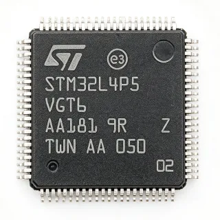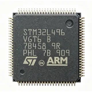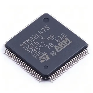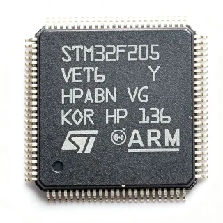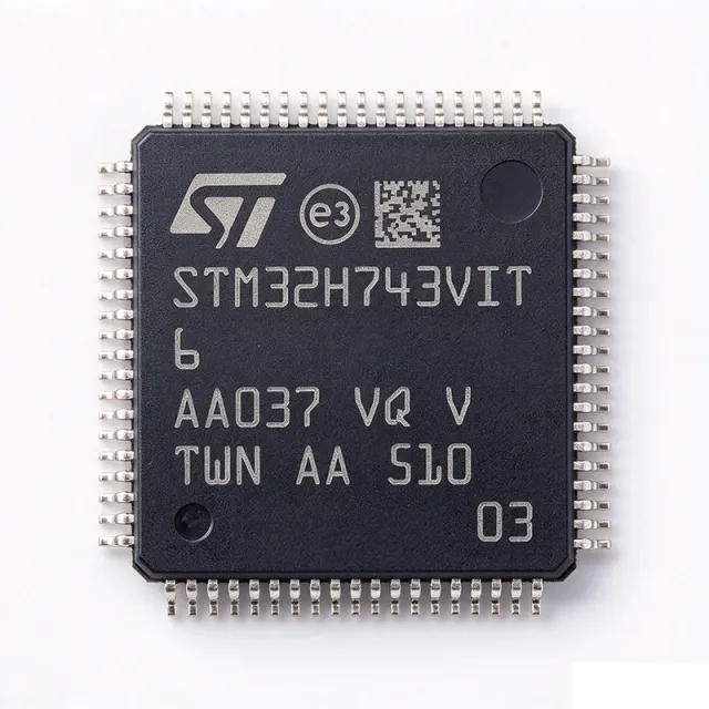
STM32H743VIT6 - 480MHz Cortex-M7 MCU 2MB Flash | ST
料号: STM32H743VIT6 ✓ 量产中| 数量 | 单价 | 小计 |
|---|---|---|
| 1 | $10.85 | $10.85 |
| 10 | $9.95 | $99.50 |
| 100 | $9.12 | $912.00 |
| 500 | $8.55 | $4,275.00 |
| 1,000 | $7.98 | $7,980.00 |
STM32H743VIT6 概述
微控制器单元(MCU)是将处理器内核、存储器和外设集成在同一芯片上的单芯片计算机。在嵌入式系统层级中,MCU 位于应用处理器之下,但高于简单的 8 位控制器,而 STM32H7 系列代表了 STMicroelectronics 广泛采用的 STM32 平台中的旗舰高性能层级。
STM32H743VIT6 的主要特性包括:带双精度 FPU 和 DSP 指令的 480 MHz Cortex-M7 内核、支持原地执行(execute-in-place)的 2 MB 片上双 bank 闪存,以及面向数据密集型工作负载的最高 1 MB SRAM。46 个通信和模拟接口可实现连接丰富型设计,无需外部桥接芯片。
在技术上,STM32H7 系列实现 Armv7-E 架构,具有 AXI 和 AHB 总线架构、ART Accelerator 和 L1 缓存以最大化从闪存执行时的内核利用率,以及由定时器、ADC、DAC 和数字通信外设组成的生态系统。多种低功耗模式可在 480 MHz 高性能与电池敏感型占空比之间取得平衡。
典型应用包括工业自动化和电机控制(利用高分辨率定时器和快速 ADC)、带图形显示器的消费类和工业 HMI(由处理余量和存储器驱动),以及使用丰富 UART、SPI、CAN 和以太网级外设组合的通信网关。
设计注意事项:LQFP-100 14x14 mm 封装在 I/O 密度与手工焊接原型制作之间取得平衡;请根据 ST 数据手册验证电源去耦,因为 480 MHz 内核运行需要低阻抗电源轨。使用 STM32CubeIDE/CubeH7 构建的固件可跨系列变体延续使用。
本页面综合了经过验证的分销商数据、同系列直接替换替代方案以及实用的采购指导,这些内容并未在 ST 数据手册中单独汇总。
直接替换替代料: STM32H743VIT6 ——相同封装,引脚兼容。需要 PCB 改动的不同封装料号已排除。
本系列中的变体
可与以下型号直接替换的同系列型号: STM32H743VIT6 (相同外形与封装尺寸) ——差异在于 Flash Memory, SRAM, Timers, ADC, Communication Interfaces.
快速对比工具——选择替代料号进行并排对比:
STM32H742VIT6
✓ 有现货
$8.5 / 个
查看数据手册 →STM32H750VBT6
✓ 有现货
$5.25 / 个
查看数据手册 →STM32H753VIT6
📋 参考替代料(不在目录中)
STM32H743VGT6
✓ 有现货
联系询价
查看数据手册 →STM32H743VIT3
📋 参考替代料(不在目录中)
STM32H743VIT6 最大额定值与电气特性
| Core Processor | ARM Cortex-M7 32-bit RISC |
| Core Frequency | 480 MHz |
| Flash Memory | 2 MB (2M x 8) |
| RAM | Up to 1 MB |
| 电源电压 | 3.3 V |
| 封装 | 100-LQFP (14x14 mm) |
| 安装类型 | Surface Mount |
| Communication & Analog Interfaces | 46 |
| Series | STM32H7 |
| 数据总线宽度 | 32 bit |
| Packaging | Tray |
STM32H743VIT6 100-lqfp (14x14 mm) 引脚配置指南
STM32H743VIT6(100-lqfp (14x14 mm) 封装)的引脚配置。 该数字 IC 包含 GPIO、通信接口(UART、SPI、I2C)和电源引脚。请参阅制造商数据手册以了解复用引脚功能和配置选项。对嵌入式系统设计和 PCB 布局至关重要。

暂无详细引脚数据: STM32H743VIT6.
请参阅 数据手册 以查看完整引脚配置。
典型应用
STM32H743VIT6 适用于 6 应用s: Industrial Automation and Motor Control, HMI and Graphical Display Systems, Communication Gateways and Protocol Converters, Test and Measurement Instrumentation, IoT Edge Nodes and Smart Sensing, Medical and Portable Diagnostic Devices.
Industrial Automation and Motor Control
The STM32H743VIT6 fits industrial automation because its 480 MHz Cortex-M7 core and 2 MB flash execute field-oriented control algorithms with ample loop-rate margin, while its fast ADCs and high-resolution timers within the 46 communication and analog interfaces enable precise current sensing and PWM generation. In a typical drive, the MCU samples phase currents, computes control loops, and drives gate-driver ICs over dedicated timer outputs, with CAN or Ethernet-class links connecting to the factory network. Performance consideration: at 480 MHz the part sustains multi-kHz control loops with interrupt headroom for protocol stacks, but layout must keep power switching noise away from the ADC reference pins.
推荐
HMI and Graphical Display Systems
Human-machine interfaces benefit directly from the STM32H743VIT6's combination of 480 MHz processing, up to 1 MB of on-chip RAM, and 2 MB of flash - enough to drive graphical UIs, decode images, and run application logic on a single chip. Its interface breadth supports SPI/parallel display connections and touch controllers, and ST's TouchGFX ecosystem targets the H7 family specifically. In practice the MCU renders UI layers and communicates with PLCs or sensors via UART/CAN. Trade-off: for very large frame buffers, external SDRAM is typically added since internal RAM alone may not hold full-resolution framebuffers, adding modest BOM cost.
推荐
Communication Gateways and Protocol Converters
The STM32H743VIT6's 46 communication and analog interfaces make it a natural protocol gateway: multiple UARTs, SPI/I2C buses, and CAN controllers run concurrently while the 480 MHz core handles protocol translation, buffering, and light TLS-grade processing. Typical designs bridge industrial CAN networks to Ethernet-adjacent backends or aggregate sensor buses into a single upstream link, with the 2 MB dual-bank flash storing multiple firmware images and configuration sets. Design consideration: dual-bank flash supports safe in-field firmware updates - a gateway that must never brick benefits from bank-swap bootloading at the cost of dedicating one flash bank.
推荐
Test and Measurement Instrumentation
Bench and portable instruments exploit the STM32H743VIT6's high core frequency, fast on-chip ADCs, and DSP-enhanced Cortex-M7 for real-time signal processing such as digital filtering, FFT analysis, and trigger decision logic. The up-to-1 MB SRAM buffers capture windows locally, and 2 MB flash retains calibration tables and instrument firmware. A typical instrument architecture pairs this MCU with front-end analog conditioning and a host interface for data upload. Performance consideration: the Art Accelerator and cache keep compute-dense DSP loops running near peak core throughput from flash, but determinism-critical code should be placed in tightly coupled memory for consistent timing.
推荐
IoT Edge Nodes and Smart Sensing
As an IoT edge node, the STM32H743VIT6 performs local analytics - anomaly detection, sensor fusion, or lightweight inference - before transmitting summaries upstream, reducing bandwidth and cloud cost. Its rich peripheral set directly interfaces MEMS sensors, and its processing headroom executes filter pipelines and protocol stacks concurrently without an external co-processor. Power-sensitive nodes duty-cycle the part through STM32H7 low-power modes between sampling events. Trade-off: the H743VIT6 is a performance-first part; ultra-low-power always-on nodes may prefer smaller STM32 L-series devices, using the H743 where local compute density justifies its consumption.
推荐
Medical and Portable Diagnostic Devices
Portable medical diagnostics use the STM32H743VIT6 for signal acquisition and on-device analysis - for example biosignal sampling where fast ADCs and the DSP-enhanced Cortex-M7 run digital filtering and feature extraction locally, keeping patient data processing inside the device. The 2 MB flash stores calibration and analysis firmware, while multiple UART/SPI interfaces connect to display modules and printers found in point-of-care instruments. Design consideration: medical designs must pair the MCU with isolated interfaces and rigorously follow the ST datasheet's power and layout guidance; verify the exact temperature-grade suffix (VIT6 standard grade) against the required operating environment specification.
推荐
推荐产品汇总
工程参考数据: STM32H743VIT6 ——对比、设计指导和合规信息。
选型指南
与替代料对比
| 参数 | 本产品 | STM32H753VIT6 | STM32H743VGT6 | STM32H742VIT6 | STM32H750VBT6 |
|---|---|---|---|---|---|
| Package | 100-LQFP (14x14 mm) | 100-LQFP (14x14 mm) - same | 100-LQFP (14x14 mm) - same | 100-LQFP (14x14 mm) - same | 100-LQFP (14x14 mm) - same |
| Brand | STMicroelectronics | STMicroelectronics | STMicroelectronics | STMicroelectronics | STMicroelectronics |
| Core / Frequency | Cortex-M7 @ 480 MHz | Cortex-M7 @ 480 MHz | Cortex-M7 @ 480 MHz | Cortex-M7 @ 480 MHz | Cortex-M7 @ 480 MHz |
| Flash Memory | 2 MB | 2 MB | 1 MB | 2 MB | 128 KB |
| RAM | Up to 1 MB | Up to 1 MB | Up to 1 MB | Up to 1 MB | Up to 1 MB |
| Hardware Crypto Acceleration | No | Yes (AES/HASH/CRYP) | No | No | No |
| Pin-to-Pin Compatibility | Reference | Pin-compatible | Pin-compatible | Pin-compatible | Pin-compatible |
| Best Fit Use Case | General high-performance embedded | Security/crypto-intensive designs | Cost-optimized with <=1 MB code | Reduced-feature industrial builds | External-flash / lowest-cost H7 |
关键差异点
- Double flash density for code-heavy applications (对比 STM32H743VGT6)
- Cost-effective general-purpose flagship vs crypto variant (对比 STM32H753VIT6)
- Retains onboard flash vs external-memory architecture (对比 STM32H750VBT6)
设计说明
A 480 MHz Cortex-M7 demands a low-impedance, well-decoupled 3.3 V supply. Follow the ST datasheet power scheme exactly for the STM32H7 series: place decoupling capacitors on every VDD/VSS pair and on the VCAP pins per the reference design, and confirm whether your board uses the internal regulator or external supply configuration appropriate for this package option. Inrush and rail sag during 480 MHz wake-up from low-power modes are common pitfalls - verify with an oscilloscope on first power-up.
The 100-pin LQFP 14x14 mm has 0.5 mm pin pitch: use solder-mask-defined pads per IPC-compatible footprints from the ST layout reference, with thermal-relief-free ground connections. Place the 0.1 uF decoupling capacitors within 2 mm of their pins and route the crystal traces short and guarded. Allocate a solid ground plane; the high core frequency makes return-path integrity directly affect EMI and ADC noise performance in mixed-signal sections of the board.
Do not confuse suffix codes: VIT6 vs VGT6 differ in flash (2 MB vs 1 MB), and temperature-grade suffixes matter for outdoor or automotive-adjacent builds. Firmware size must fit the ordered variant - CubeMX projects built on 2 MB will not link on a G-density part. Also, H7-family pin functions are heavily multiplexed: lock pin assignments in CubeMX early and re-check alternate-function tables in the datasheet before PCB routing, since peripheral instances exposed on pins vary with package pin count.
For fast peripherals (parallel display, high-speed SPI/QSPI toward external memory), keep clock and data trace lengths matched and controlled-impedance where practical. Use the internal L1 cache and Art Accelerator to run performance code from flash, but place timing-critical ISRs and DSP buffers in tightly coupled memory (TCM) for deterministic latency. Estimated: moving hot loops from cached flash to TCM typically removes tens of nanoseconds of non-deterministic access per fetch, which matters for multi-MHz control loops.
合规信息
Compliance declarations not included in the provided verified data; confirm via the official ST compliance certificate for the STM32H743VIT6 orderable part number. The part is in active production per distributor lifecycle data.