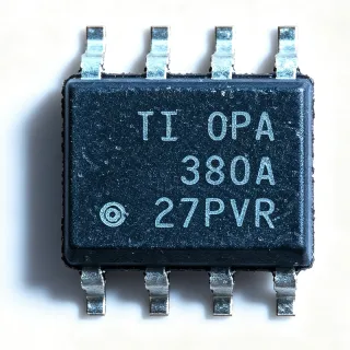
THS4042CD - 165MHz Dual High-Speed Op Amp | Texas Instruments
料号: THS4042CD ✓ 量产中THS4042CD 概述
A high-speed voltage-feedback operational amplifier is an analog signal-conditioning IC that combines wide closed-loop bandwidth with high slew rate. The THS4042 belongs to the operational-amplifier hierarchy within analog ICs, enabling rapid response to small input-voltage changes while preserving the gain and phase behavior required by feedback control loops. This is useful where conventional general-purpose amplifiers cannot preserve signal amplitude or timing through long PCB traces, cable capacitance, sampling networks, or successive-conversion systems.
The two amplifier channels provide a 165 MHz bandwidth and a 400 V/µs slew rate. These characteristics support demanding video, communications, test-and-measurement, and data-acquisition signal paths. The C-stable design allows closed-loop gains from +1 to +20 without requiring external compensation components. The device also supports driving capacitive loads, including long video lines, while its 80 dB CMRR helps reject common-mode noise coupled into the input stage.
The THS4042 uses a voltage-feedback topology designed for straightforward implementation with conventional external feedback and gain-setting resistors. Its wide bandwidth enables small-signal operation at high frequencies, while the 400 V/µs slew rate determines large-signal settling behavior. The dual-channel configuration can reduce board area when two related high-speed signals must be amplified, conditioned, or buffered.
Typical uses include driving video lines, buffering high-speed ADC inputs, amplifying communications signals, and supporting instrumentation and test-equipment front ends. For ADC buffering, the amplifier can isolate the converter from the source impedance, reducing sampling kickback. For video-line driving, the capacitive-load capability and high slew rate help preserve edge fidelity over terminated or unterminated interconnects.
PCB implementation should minimize trace lengths around the amplifier, preserve the impedance environment of high-frequency feedback loops, and provide a low-inductance ground return. Input and output placement should avoid routing critical signals beside or beneath the device. Decoupling capacitors should connect directly to the relevant supply and ground pins, while resistor networks should remain close to their associated input or feedback nodes.
This product page consolidates the manufacturer-defined bandwidth, slew-rate, channel-count, package, and application characteristics with purchasing guidance and practical implementation notes. It also distinguishes the exact THS4042CD order code from packaging or channel-count variants that are not necessarily direct substitutions.
直接替换替代料: THS4042CD ——相同封装,引脚兼容。需要 PCB 改动的不同封装料号已排除。
本系列中的变体
可与以下型号直接替换的同系列型号: THS4042CD (相同外形与封装尺寸) ——差异在于 Amplifier Type, Package.
THS4042ID
✅ 直接替换联系询价
查看数据手册 →AD826ARZ
✅ 直接替换📋 参考替代料(不在目录中)
THS4042CD 最大额定值与电气特性
| Amplifier Type | Voltage-feedback operational amplifier |
| Number of Channels | 2 channels |
| Gain-Bandwidth Product | 165 MHz |
| Slew Rate | 400 V/µs |
| Common-Mode Rejection Ratio | 80 dB |
| Compensation | C-stable |
| Capacitive Load Drive | Capable of driving capacitive loads |
| Closed-Loop Gain Support | All gains in inverting and noninverting configurations |
| 工作温度范围 | 0°C to 70°C |
| 封装 | 8-SOIC (D) |
| 引脚数 | 8 pins |
| 安装类型 | Surface mount |
THS4042CD 8-soic (d) 引脚配置指南
THS4042CD(8-soic (d) 封装)的引脚配置。 该模拟元件具有输入、输出和电源引脚。请参阅制造商数据手册以了解失调调零、补偿和使能引脚配置。适用于信号调理和放大器电路。

暂无详细引脚数据: THS4042CD.
请参阅 数据手册 以查看完整引脚配置。
典型应用
THS4042CD 适用于 6 应用s: High-Speed ADC Input Buffering, Video-Line Signal Driving, Communications Signal Conditioning, Instrumentation Front-End Amplification, Test and Measurement Signal Capture, High-Speed Clock and Data Conditioning.
High-Speed ADC Input Buffering
The THS4042CD fits between a high-speed signal source and an ADC because its 165 MHz bandwidth and 400 V/µs slew rate preserve fast transitions while the second channel can provide complementary conditioning. Its ability to drive capacitive loads helps isolate the converter input from source impedance and reduces sampling kickback into the driver. Place the device close to the ADC, use short ground returns, and account for the amplifier input capacitance when setting source and feedback impedances.
推荐
Video-Line Signal Driving
The THS4042CD is suitable for driving video lines because its 165 MHz bandwidth and 400 V/µs slew rate support rapid edge reproduction over terminated or unterminated interconnects. Its C-stable operation permits use at all closed-loop gains in noninverting and inverting configurations, while capacitive-load drive helps accommodate connector and cable loading. Preserve controlled trace geometry, provide a low-impedance return path, and verify the receiver's termination requirements to minimize reflections.
推荐
Communications Signal Conditioning
The dual THS4042CD can condition two related communications signals with 165 MHz bandwidth and a 400 V/µs slew rate. The wide small-signal bandwidth and high large-signal response support gain stages, impedance-conversion blocks, and clock-like signal paths where distortion or slow edges would impair system timing. Use one channel for the primary signal and the second for monitoring or differential support, while observing high-frequency layout practices around the SOIC-8 footprint.
推荐
Instrumentation Front-End Amplification
The THS4042CD can serve as a high-speed instrumentation front end when sensor or test signals require more bandwidth than a conventional precision amplifier provides. Its 80 dB CMRR helps suppress common-mode disturbance, while the 165 MHz bandwidth and 400 V/µs slew rate preserve rapid signal components. The dual arrangement supports paired measurement channels or an auxiliary buffer, but the application must be checked against the amplifier's complete input, output, and supply operating ranges.
推荐
Test and Measurement Signal Capture
The THS4042CD is appropriate for high-bandwidth test points where the instrument must capture or drive signals with fast edges and preserve amplitude relationships. Its 165 MHz bandwidth supports small-signal measurement bandwidth, and the 400 V/µs slew rate improves large-signal response compared with many general-purpose amplifiers. Position the amplifier near the measurement interface, keep probe and fixture capacitance controlled, and verify that the selected closed-loop gain remains stable.
推荐
High-Speed Clock and Data Conditioning
The THS4042CD can condition low-amplitude, fast-edge clock or data signals when the path requires bandwidth beyond ordinary logic-buffer limits. The 165 MHz gain-bandwidth product and 400 V/µs slew rate help maintain signal amplitude and timing through short PCB routes, while dual channels allow related control or monitoring signals to be processed together. Keep input and feedback traces short, control capacitive loading, and compare the propagated timing with the system budget.
推荐
工程参考数据: THS4042CD ——对比、设计指导和合规信息。
选型指南
与替代料对比
| 参数 | 本产品 |
|---|---|
| Amplifier Type | Dual voltage-feedback operational amplifier |
| Number of Channels | 2 channels |
| Gain-Bandwidth Product | 165 MHz |
| Slew Rate | 400 V/µs |
| Common-Mode Rejection Ratio | 80 dB |
| Compensation | C-stable |
| Closed-Loop Gain Support | All gains in inverting and noninverting configurations |
| Package | 8-SOIC (D) |
| Brand | Texas Instruments |
| Operating Temperature Range | 0°C to 70°C |
关键差异点
- Two high-speed channels in one device (对比 THS4041CD)
- C-stable operation across closed-loop gains (对比 THS4042CDG4)
- High-speed performance with capacitive-load drive (对比 THS4042CDGN)
设计说明
Place the THS4042CD adjacent to the driven load and minimize the distance from its output pin to the receiving circuit. Keep the feedback loop compact and route it away from input and output nets to prevent parasitic feedback. A continuous ground plane and short ground-return paths are preferable to long traces through or above the device. High-frequency performance depends on the physical implementation as much as the nominal 165 MHz bandwidth.
Do not treat the C-stable rating as permission to ignore loading. The amplifier can drive capacitive loads, but excessive cable, probe, connector, or ADC-input capacitance can still create ringing, overshoot, and bandwidth loss. Keep capacitance close to the device when possible, use series damping when required by the system, and validate the complete connection with oscilloscope measurements using short, low-inductance test connections.
Place each supply decoupling capacitor directly beside its corresponding power and ground pins and use the shortest possible current loop. Follow the manufacturer datasheet for the recommended capacitor values and supply arrangement. Because a 400 V/µs slew rate can produce fast output transitions, inadequate high-frequency supply impedance may couple into the output or disturb other analog circuits sharing the same supply network.
Choose external feedback and gain-setting resistors with values that preserve the intended bandwidth while limiting parasitic capacitance at the summing node. Avoid excessively large resistor values at high gain, and avoid extremely small values that increase amplifier output-current demand and power dissipation. Confirm closed-loop stability, output swing, and settling behavior using the exact gain and load configuration planned for the finished board.
合规信息
The available product information identifies an 8-SOIC commercial-temperature order code but does not provide explicit RoHS, REACH, lead-free, halogen-free, or conflict-minerals declarations for this exact MPN. AEC-Q100 qualification is not indicated and is therefore recorded as not applicable.