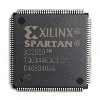
XC3S50A-4TQG144I - 50K Spartan-3A FPGA | AMD Xilinx
料号: XC3S50A-4TQG144I ✓ 量产中XC3S50A-4TQG144I 概述
A field-programmable gate array, or FPGA, is a semiconductor whose digital logic, interconnect, and I/O behavior are configured after manufacture. The XC3S50A belongs to the Spartan-3A hierarchy of low-cost FPGAs, combining programmable logic with block RAM and a high pin count. This makes it a practical platform for embedded control, protocol conversion, signal conditioning, and data acquisition where a fixed application-specific integrated circuit would be too specialized.
The principal device characteristics include 1,584 logic cells organized into 176 logic array blocks, 55,296 bits of block RAM, and 108 user I/O. Its -4 speed designation corresponds to the stated 667 MHz performance level, while the industrial I suffix identifies the extended-temperature grade. The -40 °C to 100 °C junction-temperature range supports industrial and otherwise temperature-demanding equipment, provided the board-level thermal design keeps the junction within its rated limit.
Spartan-3A devices combine programmable logic fabric, configurable I/O blocks, dedicated block RAM, and internal clocking resources on one die. The 1.2 V core architecture reduces supply requirements while leaving the I/O structure capable of supporting external system connections. Design timing, however, depends on the selected clock region, logic depth, routing congestion, I/O standards, and external timing budget, so the 667 MHz figure should not be interpreted as a guaranteed operating frequency for every design.
Typical uses include industrial automation modules with sensors and actuators, telecommunications interface equipment, embedded display and control systems, and low-cost data-acquisition products. The 108 available user I/O are particularly useful when the design must bridge multiple buses, capture parallel signals, or provide discrete control outputs while keeping the logic in reprogrammable hardware.
The principal design consideration is the 144-LQFP footprint. Place all decoupling capacitors close to the supply pins, preserve the manufacturer-defined VCC and ground connections, and assign I/O standards only through supported pins. Use the AMD Spartan-3A family data sheet for the complete pin table, configuration requirements, and board-level power sequencing before fabrication.
This page combines device specifications, application guidance, engineering design notes, and a focused replacement comparison to help engineers evaluate the XC3S50A-4TQG144I beyond a basic distributor parameter listing.
直接替换替代料: XC3S50A-4TQG144I ——相同封装,引脚兼容。需要 PCB 改动的不同封装料号已排除。
本系列中的变体
可与以下型号直接替换的同系列型号: XC3S50A-4TQG144I (相同外形与封装尺寸) ——差异在于 Package, Process Technology, Core Supply Voltage, Speed Grade, Block RAM.
XC3S50A-4TQG144C
✅ 直接替换联系询价
查看数据手册 →XC3S50A-5TQG144C
✅ 直接替换📋 参考替代料(不在目录中)
XC3S50AN-4TQG144I
✅ 直接替换📋 参考替代料(不在目录中)
XC3S50AN-4TQG144C
✅ 直接替换📋 参考替代料(不在目录中)
XC3S50-4TQG144I
✅ 直接替换联系询价
查看数据手册 →XC3S50A-4TQG144I 最大额定值与电气特性
| FPGA Family | Spartan-3A |
| System Gates | 50,000 gates |
| Configurable Logic Cells | 1,584 cells |
| Logic Array Blocks | 176 LABs/CLBs |
| Block RAM | 55,296 bits |
| User I/O | 108 I/O |
| 最大时钟频率 | 667 MHz |
| Process Technology | 90 nm CMOS |
| Core Supply Voltage | 1.2 V nominal |
| 工作电源电压 | 1.14 V to 1.26 V |
| 工作温度范围 | -40 °C to 100 °C (TJ) |
| 封装 | 144-LQFP |
| 安装方式 | SMD |
| Device Type | FPGA |
| Speed Grade | -4 |
| Temperature Grade | Industrial |
XC3S50A-4TQG144I 144-lqfp 引脚配置指南
XC3S50A-4TQG144I(144-lqfp 封装)的引脚配置。 该数字 IC 包含 GPIO、通信接口(UART、SPI、I2C)和电源引脚。请参阅制造商数据手册以了解复用引脚功能和配置选项。对嵌入式系统设计和 PCB 布局至关重要。

暂无详细引脚数据: XC3S50A-4TQG144I.
请参阅 数据手册 以查看完整引脚配置。
典型应用
XC3S50A-4TQG144I 适用于 6 应用s: Industrial Automation Controller, Parallel Data Acquisition, Telecommunications Protocol Conversion, Embedded Display Control, Motor and Encoder Interface, Instrumentation Signal Conditioning.
Industrial Automation Controller
The XC3S50A-4TQG144I fits industrial automation controllers because it combines 1,584 configurable logic cells, 176 logic array blocks, and 108 user I/O in one device. The I/O-rich 144-LQFP package can support discrete inputs, relay or transistor outputs, encoder interfaces, and diagnostic signals without requiring a separate programmable controller. Its -40 °C to 100 °C junction-temperature rating supports industrial products when enclosure temperatures and board-level thermal rise are controlled. Program the fabric for state machines, input filtering, counters, interlock logic, and communication framing. The 55,296 RAM bits also provide local buffering for cyclic process data, although a microcontroller remains useful for supervisory functions and complex external communication.
推荐
Parallel Data Acquisition
The XC3S50A-4TQG144I is well suited to parallel data-acquisition front ends because 108 user I/O can connect multiple sensor channels, clocks, and capture strobes. Its programmable logic can implement trigger delay, channel multiplexing, digital filtering, and time-aligned data packing, while 55,296 bits of block RAM support buffering between acquisition and transfer stages. The stated 667 MHz device-class performance provides timing margin for parallel logic, although actual throughput depends on routing and I/O standards. Pair the FPGA with a serial interface or microcontroller for transfer and control, and observe the 1.14 V to 1.26 V core-supply requirement during power sequencing.
推荐
Telecommunications Protocol Conversion
The XC3S50A-4TQG144I can implement compact protocol converters, framing engines, and signal-conditioning logic for telecommunications equipment. Its programmable fabric supports parallel-to-serial transformations, FIFO-based flow control, test-pattern generation, and error monitoring without requiring a complex custom ASIC. The 108 user I/O allow simultaneous access to multiple data buses and control channels, while the 144-LQFP package simplifies inspection and rework. Keep clock-domain crossings deterministic by registering synchronization stages and constraining the relevant timing paths. The industrial temperature range is useful for outdoor or rack-side equipment, subject to adequate airflow and PCB thermal design.
推荐
Embedded Display Control
The XC3S50A-4TQG144I provides enough programmable logic and I/O for embedded display timing, character generation, touch-controller scanning, and keypad multiplexing. The 108 user I/O can drive multiple display buses and accept touch or panel-control signals, while 55,296 RAM bits can hold glyph, lookup, or frame-line data. A separate microcontroller may retain the user interface, connectivity, and operating system, leaving the FPGA to accelerate display timing or scan operations. The Spartan-3A fabric is particularly useful when the interface changes during product development because logic can be updated without changing the PCB. Validate output timing against the panel specifications and account for the device's 1.2 V core supply.
推荐
Motor and Encoder Interface
The XC3S50A-4TQG144I can consolidate encoder decoding, position capture, pulse-width measurement, and step/direction control into programmable logic. Its 1,584 configurable cells provide parallel capacity for capture and conditioning, while the 108 user I/O accommodate multiple encoder channels, home sensors, and limit inputs. Block RAM can store sampled position or diagnostic traces for later transfer by a controller. The FPGA's determinism comes from clocked logic and registered interfaces rather than from the headline 667 MHz frequency alone, so constrain all timing-critical paths and account for I/O delay. The industrial temperature grade supports motor-control equipment when the enclosure's thermal conditions are managed appropriately.
推荐
Instrumentation Signal Conditioning
The XC3S50A-4TQG144I is useful in programmable instrumentation that must perform filtering, calibration, gating, and format conversion before data reaches an ADC or controller. Its programmable architecture permits reusable digital filters and threshold logic without changing hardware, while 55,296 bits of RAM support sample buffering and calibration tables. The 108 I/O enable integration of multiple measurement channels, trigger inputs, and status indicators in a single 144-LQFP device. For precision analog systems, keep the FPGA in the digital domain and use appropriate isolation or filtering at analog inputs. Synchronize asynchronous control signals before use and verify timing margins with the AMD family data sheet.
推荐
推荐产品汇总
工程参考数据: XC3S50A-4TQG144I ——对比、设计指导和合规信息。
选型指南
与替代料对比
| 参数 | 本产品 | XC3S50A-4TQG144C | XC3S50A-5TQG144C | XC3S50AN-4TQG144I | XC3S50AN-4TQG144C | XC3S50-4TQG144I |
|---|---|---|---|---|---|---|
| Brand | AMD | AMD | AMD | AMD | AMD | AMD |
| Package | 144-LQFP | 144-LQFP - same | 144-LQFP - same | 144-LQFP - same | 144-LQFP - same | 144-LQFP - same |
| FPGA Family | Spartan-3A | Spartan-3A | Spartan-3A | Spartan-3AN | Spartan-3AN | Spartan-3 |
| Speed Grade | -4 | -4 | -5 | -4 | -4 | -4 |
| Operating Temperature Range | -40 °C to 100 °C (TJ) | Commercial grade | Commercial grade | -40 °C to 100 °C (TJ) | Commercial grade | -40 °C to 100 °C (TJ) |
关键差异点
- Industrial temperature capability (对比 XC3S50A-4TQG144C)
- Matched -4 speed class with the closest same-family option (对比 XC3S50A-5TQG144C)
- Direct Spartan-3A architecture alignment (对比 XC3S50-4TQG144I)
- Higher I/O density than many related options (对比 XC3S50AN-4TQG144I)
设计说明
Design the core supply for the specified 1.14 V to 1.26 V operating range and follow the AMD family data sheet for rail sequencing and decoupling. Place the recommended bypass capacitors at the associated package power pins with short ground returns. Do not treat the nominal 1.2 V value as permission for unregulated supply tolerance; regulator droop, startup overshoot, and simultaneous I/O transitions can move the rail outside the operating limits.
The industrial suffix permits a junction-temperature range of -40 °C to 100 °C, but junction temperature is not ambient temperature. Estimated thermal analysis must use actual core current, core voltage, I/O activity, and the PCB thermal resistance. Because utilization-dependent FPGA power cannot be represented by one universal dissipation value, measure or simulate the implemented design and maintain margin below the 100 °C limit at the highest expected ambient temperature.
Use the 144-LQFP land pattern and pin table from the AMD Spartan-3A family data sheet without substituting another package drawing. Keep the device's supply and ground connections directly connected to the plane, route high-current I/O returns carefully, and avoid long stubs between external drivers and FPGA inputs. Confirm every configuration, clock, and user-I/O assignment in the final pin report before releasing the PCB for fabrication.
Treat every user I/O as a timing and signal-integrity decision rather than a generic logic connection. Select only the standards supported by the relevant Spartan-3A I/O block, account for input threshold and output-slew behavior, and use series termination where the edge rate requires it. Synchronize external asynchronous inputs before they enter multi-cycle logic, and apply explicit timing constraints to clocks, buses, and crossing boundaries.
合规信息
The manufacturer family data sheet and technical listings were used for device characteristics. Explicit compliance values were not established, so all compliance fields remain unknown.