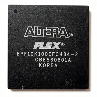
XC7A50T-1FG484I - Artix-7 FPGA, 52,160 Cells | AMD
料号: XC7A50T-1FG484I ✓ 量产中| 数量 | 单价 | 小计 |
|---|---|---|
| 1 | $0 | $0.00 |
| 10 | $0 | $0.00 |
| 100 | $0 | $0.00 |
| 500 | $0 | $0.00 |
| 1,000 | $0 | $0.00 |
XC7A50T-1FG484I 概述
What is an FPGA? A field-programmable gate array is a reconfigurable digital semiconductor in the programmable-logic and FPGA category. Instead of fixing the logic at fabrication, engineers configure an FPGA after manufacture using HDL synthesis, place-and-route tools, and a device bitstream. Within the hardware hierarchy, the XC7A50T belongs to the Artix-7 FPGA family and provides a programmable-logic platform for control, signal processing, communications, and embedded-system logic.
The supplied AMD-related search data identifies the device as an Artix-7 FPGA with 52,160 logic cells in a 484-BBGA package. The available comparison data also states 28 nm CMOS technology and a 1 V operating value for the target MPN. The -1 ordering code is commonly used to identify the speed grade, but the supplied data does not provide a complete timing table, I/O standards, block-resource counts, pinout, or absolute maximum ratings. Those parameters must therefore be confirmed against the manufacturer documentation before release.
The 484-BBGA package is suited to compact, high-pin-count boards where a large number of package balls are required. Unlike a cross-package replacement, any proposed alternative must use the same package footprint and preserve the relevant ball assignments, voltage requirements, configuration interface, and design-tool compatibility. The supplied cross-reference results identify same-family 484-pin candidates, but they do not provide enough verified detail to establish five unqualified production drop-in replacements.
Typical engineering uses include industrial automation, embedded control, sensor and signal-processing front ends, communications infrastructure, and general-purpose digital prototyping. The device should be paired with a validated power architecture, decoupling strategy, clocking plan, configuration memory or boot source, and AMD FPGA implementation flow. Because the provided evidence does not contain the complete pinout or timing specifications, PCB and firmware decisions should not be based on search-result snippets alone.
For a new design, the target MPN is best suited when its documented resources, speed grade, temperature range, and package assignments match the design. For an existing PCB, compare the exact package suffix, ball map, core voltage, I/O voltage, configuration pins, memory interfaces, and required IP before considering a replacement. The official AMD Artix-7 package-pinout resources are the authoritative starting point for these checks.
This page consolidates the verified search results, package identity, sourcing links, and design cautions for XC7A50T-1FG484I. It also separates documented values from missing engineering data rather than presenting inferred specifications as facts.
直接替换替代料: XC7A50T-1FG484I ——相同封装,引脚兼容。需要 PCB 改动的不同封装料号已排除。
快速对比工具——选择替代料号进行并排对比:
XC7A50T-1FGG484I
✅ 直接替换📋 参考替代料(不在目录中)
XC7A50T-1FGG484C
✅ 直接替换📋 参考替代料(不在目录中)
XC7A50T-1FGG484I4977
✅ 直接替换📋 参考替代料(不在目录中)
XC7A50T-1FG484I 最大额定值与电气特性
| Device Type | Artix-7 Field Programmable Gate Array (FPGA) |
| Programmable Logic Cells | 52,160 cells |
| 封装 | 484-BBGA |
| Package Pin Count | 484 balls |
| Technology | 28 nm CMOS |
| Operating Voltage | 1 V |
| Speed Grade | -1 |
| Temperature Grade | Industrial |
| 安装类型 | Surface Mount |
| Product Category | FPGAs |
| Manufacturer | Advanced Micro Devices |
| Manufacturer Brand | AMD / Xilinx |
XC7A50T-1FG484I 484 balls 引脚配置指南
XC7A50T-1FG484I(484 balls 封装)的引脚配置。 该数字 IC 包含 GPIO、通信接口(UART、SPI、I2C)和电源引脚。请参阅制造商数据手册以了解复用引脚功能和配置选项。对嵌入式系统设计和 PCB 布局至关重要。

暂无详细引脚数据: XC7A50T-1FG484I.
请参阅 数据手册 以查看完整引脚配置。
典型应用
XC7A50T-1FG484I 适用于 6 应用s: Industrial Automation Control, Embedded Signal Processing, Communications Interface, Sensor Fusion Node, High-Speed Data Acquisition, Programmable Logic Prototype.
Industrial Automation Control
XC7A50T-1FG484I fits programmable industrial automation when a design needs a compact 484-BBGA FPGA with 52,160 logic cells. The FPGA can implement sequencing, state machines, data acquisition control, interlocks, and communications framing while its 28 nm CMOS process supports a modern programmable-logic implementation. The -1 speed grade and industrial-temperature suffix are useful selection points, but the supplied data does not specify the numeric temperature limits or exact I/O standards. Engineers should confirm clock rates, I/O voltage domains, and package ball assignments against the official AMD documentation before placing it in a PLC-like controller.
推荐
Embedded Signal Processing
The Artix-7 XC7A50T-1FG484I is suitable for embedded signal-processing front ends that need programmable filtering, event detection, or timing logic close to an external converter. Its 52,160-cell resource level provides more room than a small logic device, while the 484-BBGA package exposes a high-density interface for converters, memories, and control signals. The supplied evidence does not provide DSP-slice counts, block RAM, maximum clock frequency, or I/O standard coverage, so those constraints must be checked in the manufacturer datasheet. A practical design should preserve timing margin and isolate analog or high-speed routing.
推荐
Communications Interface
XC7A50T-1FG484I can be evaluated for communications-interface logic that needs programmable framing, CRC handling, buffering, or protocol adaptation. The 52,160-cell Artix-7 device and 484-BBGA package offer substantial logic and package density for medium-complexity interface bridges, provided the exact I/O assignments and timing meet the system requirement. The supplied data does not identify supported transceiver standards, memory-interface widths, or maximum I/O rates. Use the AMD package-pinout files and timing documentation to assign voltage domains, implement constraints, and confirm that the selected external PHY or transceiver is compatible with the chosen FPGA I/O standards.
推荐
Sensor Fusion Node
The XC7A50T-1FG484I is a candidate for sensor-fusion nodes that combine multiple digital sensors, timestamp logic, filtering, and local decision-making. Its 52,160 programmable logic cells provide a higher-density platform than a basic microcontroller while preserving parallel I/O flexibility. The supplied data does not confirm analog inputs, ADC resources, sensor interfaces, or package-level differential I/O assignments, so the FPGA would likely require external converters and interface devices. The industrial-temperature suffix supports early evaluation for factory environments, subject to confirming the actual numeric temperature rating and environmental qualification.
推荐
High-Speed Data Acquisition
XC7A50T-1FG484I may be used as the control and capture fabric in a high-speed data-acquisition system when its documented I/O and timing resources satisfy the converter interface. The 484-BBGA package provides many package balls for parallel data, clock, control, and memory connections, while the Artix-7 architecture supports programmable acquisition sequencing and real-time processing. The provided search data does not establish maximum pin rates, supported voltage standards, clock-management resources, or memory interfaces. These missing details are decisive for this application, so use the manufacturer timing tables and Vivado implementation reports before committing to the part.
推荐
Programmable Logic Prototype
XC7A50T-1FG484I is useful for programmable-logic prototypes because the Artix-7 family provides a larger implementation target than small CPLDs while retaining a 484-BBGA package option for complex boards. Designers can use the device to validate state machines, parallel datapaths, control logic, or interface bridging before committing to a larger FPGA. The supplied evidence does not include development-board availability, tool-version support, or resource-specific limits. A prototype should include a defined clock and reset plan, verified power rails, accessible configuration storage, and test points for debugging high-speed or high-density ball connections.
推荐
推荐产品汇总
工程参考数据: XC7A50T-1FG484I ——对比、设计指导和合规信息。
选型指南
与替代料对比
| 参数 | 本产品 | XC7A50T-1FGG484I | XC7A50T-1FGG484C | XC7A50T-1FGG484I4977 |
|---|---|---|---|---|
| Device Type | Artix-7 FPGA | Artix-7 FPGA | Artix-7 FPGA | Related 484-BBGA listing; exact device classification not established |
| Package | 484-BBGA | 484-BBGA - same package family | 484-BBGA - same package family | 484-BBGA - same package family |
| Brand | AMD / Xilinx | AMD / Xilinx | AMD / Xilinx | AMD / Xilinx |
| Verified Numeric Price | Not provided | Not provided | Not provided | Not provided |
关键差异点
- Exact target identity (对比 XC7A50T-1FGG484I)
- Package continuity for a PCB upgrade (对比 XC7A50T-1FGG484C)
- Design-resource positioning (对比 XC7A50T-1FGG484I4977)
设计说明
Design the power rails from the exact AMD electrical tables for XC7A50T-1FG484I. The supplied search data identifies a 1 V operating value, but it does not establish the complete core and I/O voltage ranges, tolerance, sequencing, or current limits. Separate the core, auxiliary, and user-I/O supplies where required by the device data, provide local decoupling at every supply ball group, and verify startup sequencing with the configuration mechanism. Do not infer the complete power tree from the single 1 V search-result value.
Use the official 484-BBGA package drawing and Artix-7 package-pinout files before placing the device. A 484-BBGA footprint has many balls with configuration, clock, power, ground, and user-I/O functions; an apparently similar package name does not guarantee the same ball map. Keep high-speed routes short, provide a solid ground reference, route supply and ground connections with low impedance, and include test access for configuration, reset, clock, and representative I/O signals. Recheck every alternative against the exact package suffix rather than relying on the generic 484-pin label.
Do not treat a related MPN as a drop-in replacement solely because the family name and 484-BBGA package appear similar. Confirm the ordering table, package suffix, speed grade, temperature grade, pin assignments, supported voltage standards, configuration pins, and resource compatibility. The supplied cross-reference results explicitly caution that same-series or same-package candidates require datasheet and pinout checks. After any substitution, rerun Vivado implementation and timing analysis, then perform hardware bring-up with the original configuration and I/O test patterns.
合规信息
The supplied web data does not state RoHS, REACH, AEC-Q100, lead-free, halogen-free, or conflict-minerals status for XC7A50T-1FG484I. Compliance must be confirmed from the manufacturer product declaration or authorized supply documentation.