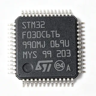
STM32L072CZT6 - 192KB Flash Cortex-M0+ MCU | STMicroelectronics
MPN: STM32L072CZT6 ✓ نشطSTM32L072CZT6 نظرة عامة
An ARM Cortex-M0+ microcontroller (MCU) is a 32-bit RISC processor core from ARM's Cortex-M family optimized for energy efficiency and deterministic interrupt response in deeply embedded systems. The Cortex-M0+ sits at the low-power end of the Cortex-M lineup (Cortex-M0+ -> Cortex-M0 -> Cortex-M3/M4/M33), and STM32L0 microcontrollers sit at the low-power end of the STM32 product hierarchy (STM32L0 -> STM32L1/L4/L5 -> STM32F/G/H families). L0-series MCUs target coin-cell, sensor, metering, and wearable designs where standby current and integrated analog peripherals matter more than raw compute throughput.
Key features of the STM32L072CZT6 include 192 KB Flash with ECC, 20 KB SRAM, a 12-bit ADC with hardware oversampling, two ultra-low-power comparators, a real-time clock, multiple timers, and a USB 2.0 full-speed device interface that operates without an external crystal. The device supports AES-128 hardware encryption for secure connectivity in IoT endpoints. Integrated peripherals include I2C, SPI, USART, USB, and capacitive-touch sensing I/Os.
The architecture combines a Cortex-M0+ core with ST's ultra-low-power design techniques, including multiple voltage domains, low-power RTC, and a wide set of GPIOs tolerant to 5 V. The 48-pin LQFP package balances compact board footprint with easy hand-soldering and breadboard prototyping, and supports the full STM32L072xx peripheral set on the available I/O count.
Typical applications include battery-powered IoT sensors, USB-connected wearables, smart metering endpoints, wireless sensor nodes, medical patch devices, asset trackers, and human-machine interface panels. Designers value the part for USB connectivity in small form factors, deep-sleep currents, and an established STM32 toolchain (STM32CubeIDE, HAL/LL libraries). When designing with this part, plan decoupling around the 1.2 V core regulator pin and verify the low-power mode transitions in your application firmware before committing to battery-life calculations.
بدائل مباشرة لـ STM32L072CZT6 — نفس الحزمة، متوافق دبوس بدبوس. تُستثنى القطع ذات الحزم المختلفة التي تتطلب تعديل PCB.
الطرازات في هذه السلسلة
طرازات من نفس السلسلة متوافقة تمامًا مع STM32L072CZT6 (نفس عامل الشكل والبصمة) — يختلف في ADC, Communication Interfaces, Core, Timers.
STM32L073CZT6
✅ بديل مباشر📋 بديل مرجعي (غير موجود في الكتالوج)
STM32L072CZT3
✅ بديل مباشر📋 بديل مرجعي (غير موجود في الكتالوج)
STM32L072CZT6D
✅ بديل مباشر📋 بديل مرجعي (غير موجود في الكتالوج)
STM32L053CZT6
✅ بديل مباشر📋 بديل مرجعي (غير موجود في الكتالوج)
STM32L083CZT6
✅ بديل مباشر📋 بديل مرجعي (غير موجود في الكتالوج)
STM32L072CZT6 الحدود القصوى والخصائص الكهربائية
| Core | ARM Cortex-M0+ (32-bit) |
| أقصى تردد للساعة | 32 MHz |
| Flash Memory | 192 KB |
| SRAM | 20 KB |
| Supply Voltage (VDD) | 1.65 V to 3.6 V |
| Supply Voltage (BOR enabled) | 1.8 V to 3.6 V |
| درجة حرارة التشغيل | -40 C to +85 C (grade 6) |
| العلبة | 48-pin LQFP (7x7 mm) |
| نوع التركيب | Surface Mount |
| USB | USB 2.0 full-speed device (crystal-less) |
| ADC | 12-bit, hardware oversampling |
| Comparators | 2 ultra-low-power comparators |
| Timers | Multiple 16-bit and 32-bit timers (see datasheet) |
| Communication Interfaces | I2C, SPI, USART, USB |
| AES Hardware | AES-128 |
| RTC | Yes, with calendar and tamper |
| I/Os | Up to 37 GPIOs (package-dependent) |
| حالة RoHS | Compliant |
تكوين أطراف STM32L072CZT6
| دبوس 1 | PB9 — GPIO PB9 / I2C1_SDA |
| دبوس 2 | PB10 — GPIO PB10 / I2C2_SDA |
| دبوس 3 | PB11 — GPIO PB11 / I2C2_SCL |
| دبوس 4 | VDD — Digital supply voltage |
| دبوس 5 | PB12 — GPIO PB12 / SPI2_NSS |
| دبوس 6 | PB13 — GPIO PB13 / SPI2_SCK |
| دبوس 7 | PB14 — GPIO PB14 / SPI2_MISO |
| دبوس 8 | PB15 — GPIO PB15 / SPI2_MOSI |
| دبوس 9 | PA8 — GPIO PA8 |
| دبوس 10 | PA9 — GPIO PA9 / USART1_TX |
| دبوس 11 | PA10 — GPIO PA10 / USART1_RX |
| دبوس 12 | PA11 — GPIO PA11 / USB_DM |
| دبوس 13 | PA12 — GPIO PA12 / USB_DP |
| دبوس 14 | PA13 — GPIO PA13 / SWDIO |
| دبوس 15 | VSS — Digital ground |
| دبوس 16 | VDD — Digital supply voltage |
| دبوس 17 | PA14 — GPIO PA14 / SWCLK |
| دبوس 18 | PA15 — GPIO PA15 / JTDI |
| دبوس 19 | PB3 — GPIO PB3 / JTDO |
| دبوس 20 | PB4 — GPIO PB4 / NJTRST |
| دبوس 21 | PB5 — GPIO PB5 |
| دبوس 22 | PB6 — GPIO PB6 / I2C1_SCL |
| دبوس 23 | PB7 — GPIO PB7 / I2C1_SDA |
| دبوس 24 | PB8 — GPIO PB8 |
| دبوس 25 | VSS — Digital ground |
| دبوس 26 | VDD — Digital supply voltage |
| دبوس 27 | PC13 — GPIO PC13 / RTC_TAMP |
| دبوس 28 | PC14 — GPIO PC14 / OSC32_IN |
| دبوس 29 | PC15 — GPIO PC15 / OSC32_OUT |
| دبوس 30 | VSS — Digital ground |
| دبوس 31 | VDDA — Analog supply voltage |
| دبوس 32 | VREF+ — ADC reference voltage |
| دبوس 33 | PA0 — GPIO PA0 / ADC_IN0 |
| دبوس 34 | PA1 — GPIO PA1 / ADC_IN1 |
| دبوس 35 | PA2 — GPIO PA2 / ADC_IN2 / USART2_TX |
| دبوس 36 | PA3 — GPIO PA3 / ADC_IN3 / USART2_RX |
| دبوس 37 | PA4 — GPIO PA4 / ADC_IN4 |
| دبوس 38 | PA5 — GPIO PA5 / ADC_IN5 |
| دبوس 39 | PA6 — GPIO PA6 / ADC_IN6 |
| دبوس 40 | PA7 — GPIO PA7 / ADC_IN7 |
| دبوس 41 | PC0 — GPIO PC0 / ADC_IN10 |
| دبوس 42 | PC1 — GPIO PC1 / ADC_IN11 |
| دبوس 43 | PC2 — GPIO PC2 / ADC_IN12 |
| دبوس 44 | PC3 — GPIO PC3 / ADC_IN13 |
| دبوس 45 | VSSA — Analog ground |
| دبوس 46 | VREF- — ADC reference ground |
| دبوس 47 | VSS — Digital ground |
| دبوس 48 | VDD — Digital supply voltage |
التطبيقات النموذجية
STM32L072CZT6 مناسب لـ 6 التطبيقs: Battery-Powered IoT Sensor Nodes, USB-Connected Wearable Devices, Smart Metering Endpoints, Medical Patch and Health Monitoring Devices, Asset Tracking and Cold-Chain Loggers, Human-Machine Interface Panels.
Battery-Powered IoT Sensor Nodes
The STM32L072CZT6 fits battery-powered IoT sensor nodes because of its sub-microamp Standby current (sub-uA) and 192 KB Flash for sensor-stack firmware. Its 32 MHz Cortex-M0+ core is fast enough for periodic sensor sampling while sleeping deeply between events, which directly extends CR2032 coin-cell life. According to the ST datasheet, Stop mode with RTC draws less than 1 uA, enabling multi-year battery deployments for environmental sensors.
موصى به
USB-Connected Wearable Devices
The STM32L072CZT6 is well matched to USB-connected wearables because of its crystal-less USB 2.0 full-speed device interface and 192 KB Flash for vendor-class USB stacks. Designers save a 48 MHz crystal and reduce BOM cost while maintaining USB compliance, per the ST datasheet. The LQFP-48 package fits on small wearable PCAs with 5 V-tolerant GPIOs for charger integration.
موصى به
Smart Metering Endpoints
Smart metering applications benefit from the STM32L072CZT6's RTC with calendar, tamper detection, AES-128 hardware encryption, and 12-bit ADC for voltage/current sensing. The part's wide 1.65-3.6 V supply supports battery-backed meter designs, and the LQFP-48 footprint provides enough I/Os for meter interfaces. According to the datasheet, AES-128 hardware runs at low power without CPU overhead, securing AMI traffic.
موصى به
Medical Patch and Health Monitoring Devices
The STM32L072CZT6 suits medical patch devices thanks to its low-power modes, 12-bit ADC with hardware oversampling, and 192 KB Flash for DSP-style signal processing. According to the ST datasheet, the 12-bit ADC reaches 16-bit effective resolution with oversampling, supporting accurate bio-potential measurements. The LQFP-48 package is small enough for wearable form factors and has 5 V-tolerant GPIOs for sensor interfacing.
موصى به
Asset Tracking and Cold-Chain Loggers
Cold-chain and asset tracking applications benefit from the STM32L072CZT6's RTC calendar, low-power Stop mode, AES-128 for signed log integrity, and 192 KB Flash for local storage of time-stamped events. The 32 MHz Cortex-M0+ core is sufficient to drive temperature/humidity sampling and USB-based log extraction in field service. Per ST documentation, the part handles -40 C to +85 C industrial environments.
موصى به
Human-Machine Interface Panels
The STM32L072CZT6 supports HMI panel designs with its capacitive-touch sensing I/Os, 12-bit ADC for analog slider feedback, AES-128 for secure boot, and 192 KB Flash for graphics state machines. The LQFP-48 footprint provides sufficient I/O count for keypad scanning plus LCD segment driving via external drivers. The crystal-less USB interface supports field firmware updates without an external oscillator.
موصى به
ملخص المنتجات الموصى بها
بيانات مرجعية هندسية لـ STM32L072CZT6 — المقارنة وإرشادات التصميم ومعلومات الامتثال.
دليل الاختيار
المقارنة مع البدائل
| المعامل | هذا المنتج | STM32L073CZT6 | STM32L072CZT3 | STM32L072CZT6D | STM32L053CZT6 | STM32L083CZT6 |
|---|---|---|---|---|---|---|
| Package | LQFP-48 (7x7 mm) | LQFP-48 (7x7 mm) - same | LQFP-48 (7x7 mm) - same | LQFP-48 (7x7 mm) - same | LQFP-48 (7x7 mm) - same | LQFP-48 (7x7 mm) - same |
| Brand | STMicroelectronics | STMicroelectronics | STMicroelectronics | STMicroelectronics | STMicroelectronics | STMicroelectronics |
| Flash Memory | 192 KB | 192 KB | 192 KB | 192 KB | 192 KB | 192 KB |
| SRAM | 20 KB | 20 KB | 20 KB | 20 KB | 20 KB | 20 KB |
| USB Peripheral | Yes (crystal-less USB 2.0 FS) | Yes | Yes | Yes | No | Yes |
| AES-128 Hardware | Yes | Yes | Yes | Yes | Yes | Yes |
| Wireless Connectivity | None | Sigfox | None | None | None | LoRa |
| Operating Temperature | -40 C to +85 C | -40 C to +85 C | -40 C to +125 C | -40 C to +85 C | -40 C to +85 C | -40 C to +85 C |
| Supply Voltage | 1.65 V to 3.6 V | 1.65 V to 3.6 V | 1.65 V to 3.6 V | 1.65 V to 3.6 V | 1.65 V to 3.6 V | 1.65 V to 3.6 V |
أبرز الفروقات
- Crystal-less USB 2.0 full-speed peripheral (مقابلSTM32L053CZT6)
- Optional wireless connectivity without PCB rework (مقابلSTM32L073CZT6)
- 192 KB Flash headroom for USB stacks (مقابلSTM32L052C8T6)
ملاحظات التصميم
Estimated: at 32 MHz active core current with peripherals disabled the STM32L072CZT6 draws around 1 mA/MHz per ST datasheet figures. Add 100 nF + 10 uF ceramic decoupling near each VDD/VDDA pin and a ferrite bead between digital and analog supplies for clean ADC readings. Use the integrated voltage regulator to drive VDD from a 1.8 V to 3.3 V rail and avoid supplying core voltage externally.
At low duty cycles the STM32L072CZT6 spends nearly all its time in Stop or Standby, so self-heating is negligible. For continuous-active designs at 32 MHz, the LQFP-48 theta_JA around 65 C/W produces only a few degrees of rise even without a copper pour. Still place thermal vias under the exposed pad if your PCB stackup supports it.
Route the USB DP/DM pair (PA11/PA12) as a 90 ohm differential with length matching within 150 mils and keep them away from switching nodes. The crystal-less USB relies on internal trimming, so a clean 3.3 V rail with low ripple is essential. Per ST AN4879, place the USB common-mode choke near the connector side of the route.
Do not exceed 3.6 V on any pin including 5 V-tolerant GPIOs. Make sure BOOT0 is tied low for normal Flash boot and pulled high only for system memory bootloader access. Disable unused peripherals in PWR register settings before entering Stop mode to achieve sub-microamp current per the ST reference manual RM03510.
معلومات الامتثال
RoHS and REACH compliance per ST product page. Not AEC-Q100 qualified - this is a commercial/consumer part. For automotive applications use the equivalent -A or -Q suffix variant if available.