DC-DC Converters
Products (207)
TPS62810QWRWYRQ1 - 4A Automotive Buck Converter | TI
The Texas Instruments TPS62810QWRWYRQ1 is an automotive-grade synchronous step-down DC/DC converter delivering up to 4A of continuous output current from a 2.75V to 6V input, with an adjustable output voltage starting from 0.6V. It is housed in a compact 2mm x 3mm VQFN-9 (RWY) package with wettable flanks for enhanced solder-joint inspection in automotive manufacturing. A synchronous buck converter is a type of switching voltage regulator that steps down a higher input voltage to a lower output voltage with high efficiency, typically above 90%. Within the power management IC hierarchy, buck converters sit alongside LDOs and boost converters and are preferred whenever load current or efficiency demands exceed what a linear regulator can dissipate. The TPS62810QWRWYRQ1 belongs to the TPS6281x-Q1 family of pin-to-pin 1A, 2A, 3A, and 4A automotive converters. Key features include AEC-Q100 qualification (temperature grade 1, -40C to +125C ambient), Functional Safety-Capable documentation to support ISO 26262 system design, and peak current mode control topology for fast transient response. Low-resistive integrated switches minimize conduction losses, while the adjustable switching frequency can be synchronized to an external clock to control EMI. A power-good output, enable pin, and soft-start support robust power sequencing in multi-rail systems. The device is designed for automotive applications such as infotainment and advanced driver assistance systems (ADAS). Reference designs pair the TPS62810-Q1 with an LM63635-Q1 bus converter switching at 2.1 MHz, with the load converters switching at 2.2 MHz to ease filtering. Typical rails include core supplies for processors, camera and radar modules, and communication modules in vehicles. When designing with this converter, choose input and output capacitors and the inductor per the datasheet guidelines to maintain stability and minimize output ripple. Use thermal vias under the exposed pad to optimize heat dissipation at full 4A load.
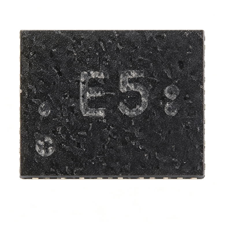
TPS62840DLCR - 60nA IQ Buck 750mA 8-VFDFN | Texas Instruments
The Texas Instruments TPS62840DLCR is a high-efficiency step-down (buck) converter operating from a 1.8 V to 6.5 V input and delivering up to 750 mA output current in an 8-pin VFDFN (DLC) package measuring 3.0 mm x 3.0 mm. A buck converter, or step-down converter, is a switching DC-DC regulator that efficiently converts a higher voltage to a lower voltage using switching MOSFETs and an inductor, sitting within the hierarchy: buck converter -> DC-DC converter -> voltage regulator -> power management IC. Key features include an ultra-low 60 nA operating quiescent current, critical for always-on and standby-dominated battery systems. Special circuitry achieves just 120 nA IQ in 100% duty-cycle mode, extending battery life near end-of-discharge. The DCS-Control(TM) topology combines voltage-mode and current-mode control for clean RF powering and seamless PWM-to-Power-Save-Mode transition. The device achieves 80% efficiency at a 1 uA load (3.6 VIN to 1.8 VOUT), and the typical 1.8 MHz switching frequency permits small inductors and capacitors for a compact solution. Technically, the TPS62840 integrates high-side and low-side MOSFETs, a control loop, and a precision reference. In Power-Save Mode the switching frequency reduces at light load to maintain efficiency. A STOP pin immediately disables switching to eliminate noise in test and measurement systems. Soft-start, overcurrent protection, and thermal shutdown are integrated. The output voltage is adjustable via an external resistor divider. Typical applications include battery-powered IoT sensors, wearable devices, wireless earbuds, smart meters, and energy-harvesting systems, as well as powering RF transceivers and microcontrollers. The wide input range supports 2S-4S alkaline, 1S-2S Li-MnO2, and 1S Li-Ion/Li-Polymer chemistries. Design tip: use approximately 10 uF input and 22 uF output capacitance placed close to the IC, select the inductor for 1.8 MHz operation, and use the STOP pin during noise-sensitive measurements.
TPS63021 - 4A Switch Buck-Boost Converter | Texas Instruments
The Texas Instruments TPS63021 is a high-efficiency, single-inductor buck-boost converter with 4A switches, designed to provide a regulated output voltage from input sources that can be above or below the output. It supports output currents up to 3A and is available in a 14-pin VFDFN (DSJ) package with exposed thermal pad. The device operates from input voltages ranging from 1.8V to 5.5V, making it suitable for battery-powered applications using two or three alkaline, NiCd, or NiMH cells, or a single Li-ion or Li-polymer cell. A buck-boost converter is a type of DC-DC converter that can step up (boost) or step down (buck) the input voltage to maintain a constant output voltage, regardless of whether the input is higher or lower than the output. This is essential in battery-powered systems where the battery voltage declines over time, falling below the required rail voltage. The TPS63021 belongs to the power management IC family, specifically within DC-DC converters, and is a key component in portable electronics. Key features include a fixed 3.3V output voltage, high efficiency up to 96%, and a low quiescent current of 50 µA. The device integrates synchronous rectification, which eliminates the need for an external Schottky diode, improving efficiency and reducing component count. It also features load disconnect, light-load efficiency, and undervoltage lockout (UVLO) with fixed thresholds. The TPS63021 operates over a junction temperature range of -40°C to +125°C. Technically, the TPS63021 uses a proprietary control architecture that seamlessly transitions between buck and boost modes, ensuring stable output voltage with minimal ripple. The 4A switches allow for high output currents, and the device can deliver up to 3A in boost mode from a 3.3V input. The VFDFN package with exposed pad provides excellent thermal performance, with a thermal resistance of 40°C/W, enabling compact designs without external heatsinks. Typical applications include portable electronics, battery-powered devices, and systems powered by supercapacitors. The TPS63021 is ideal for powering microcontrollers, sensors, and wireless modules in IoT devices, where input voltage varies widely. Its high efficiency extends battery life, and its small footprint saves board space. When designing with the TPS63021, ensure proper input and output capacitor selection to minimize ripple and maintain stability. Use low-ESR ceramic capacitors with sufficient voltage rating. The exposed pad must be soldered to a thermal land on the PCB for optimal heat dissipation.
TPS63070RNMT - 2V-16V, 2A Buck-Boost Converter | TI
The Texas Instruments TPS63070RNMT is a high-efficiency, wide-input buck-boost DC-DC switching regulator that maintains a regulated output whether the input is above or below the target. It operates from 2V to 16V input, delivers up to 2A output current, and provides an adjustable output of 2.5V to 9V in a compact 15-pin VQFN-HR (RNM) package with -40C to +125C junction operation. A buck-boost converter is a type of DC-DC switching regulator within the broader power management IC category that combines buck (step-down) and boost (step-up) topologies. This lets a single inductor-based stage produce a stable rail from sources such as 4-cell alkaline, 12V lead-acid, or solar inputs whose voltage swings across the output level. The TPS63070 belongs to the switching voltage regulator family used in portable, industrial, and IoT power systems. Key features include a 3.6A switch current limit, 2.4MHz switching frequency, and low quiescent current of approximately 50uA typical. Synchronous rectification with integrated MOSFETs improves efficiency and reduces external component count, while the 2.4MHz clock permits small inductors and capacitors for a compact footprint. PWM mode maximizes heavy-load efficiency and PFM mode preserves light-load efficiency; the device also supports negative output current sinking in PWM mode per TI datasheet SLVSDD7B. Architecture-wise, the four-switch synchronous buck-boost topology seamlessly transitions between buck, buck-boost, and boost operating regions with a single inductor, avoiding output discontinuity when the battery voltage crosses the setpoint. The adjustable feedback (FB) pin sets the output with a resistor divider, and programmable soft-start limits inrush current. Typical applications include battery-powered portable instruments, industrial sensors, IoT wireless nodes, and 12V rail conditioning for microcontrollers, RF modules, and displays. Wide input tolerance makes it ideal for solar or vehicle-supplied systems. For best results, keep the inductor and input/output capacitor loops short, place the input capacitor at VIN and PGND, and provide adequate copper on the thermal pad. Pricing references are as of 2026-08-28.
TPS63710 - 1A Low Noise Inverting Buck Converter | TI
The Texas Instruments TPS63710 (TPS63710DRRR) is a low-noise synchronous inverting buck converter that generates a negative output voltage down to -5.5 V from a positive input of 3.1 V to 14 V, delivering up to 1 A of output current depending on the input-to-output voltage ratio. It is packaged in a 3-mm x 3-mm 12-pin WSON with exposed pad (12-WFDFN), providing excellent thermal performance for space-constrained designs. An inverting buck converter is a type of DC-DC switching regulator that produces a negative output rail from a positive supply. It belongs to the broader family of switching voltage regulators within power management ICs, which convert and regulate voltages efficiently using inductive energy storage rather than the dissipative approach of linear regulators. This makes inverting buck converters well suited to battery-powered and higher-current negative-rail applications where charge pumps cannot supply enough current. Key features of the TPS63710 include a filtered reference system with an external capacitor on the CAP pin that suppresses low-frequency 1/f noise up to approximately 100 kHz, a performance level required in high-performance telecommunication systems. The fixed-frequency PWM control topology gives predictable switching behavior and simple EMI filtering. Synchronous rectification eliminates the external Schottky diode, improving efficiency and reducing bill-of-material count. An enable pin supports power sequencing, and integrated soft-start limits inrush current. The device targets applications requiring a clean negative rail, such as op-amp supply rails, data converters, RF transceivers, bias supplies for GaN amplifiers, and optical modules. Its low-noise reference system makes it suitable for powering sensitive analog circuitry where output ripple and noise degrade signal integrity, while the wide input range supports both 5 V and 12 V system rails. When designing with the TPS63710, select input and output capacitors and an inductor with adequate saturation current to maintain stability and handle peak currents, and solder the exposed thermal pad to a copper area for heat dissipation. As of 2026-08-29, single-unit pricing from distributors starts near $1.51 (LCSC), with stock available at DigiKey, Mouser, and LCSC.
TPS63710DRRR - 1A Inverting Buck Converter -5.5V | TI
The Texas Instruments TPS63710 is a low-noise synchronous inverting buck DC-DC converter that generates a negative output voltage down to -5.5 V from a positive input rail, delivering up to 1 A of output current depending on the input-voltage to output-voltage ratio. It is supplied in a 12-pin VSON/WFDFN exposed-pad package (TPS63710DRRR in reel packaging). An inverting buck converter, sometimes called a negative buck or inverting step-down converter, is a switching power converter topology that produces a regulated negative output voltage from a positive supply. Within the power management IC hierarchy, it belongs to the family of DC-DC switching regulators, sitting alongside buck, boost, and inverting charge pump converters. Unlike charge pump inverters, an inverting buck can deliver ampere-class currents with high efficiency. Key features include the negative adjustable output down to -5.5 V, up to 1 A output current, and a fixed-frequency PWM control topology for predictable EMI behavior. Its most distinctive feature is the filtered reference system: an external filter capacitor on the CAP pin suppresses low-frequency (1/f) noise from the lower frequency limit up to around 100 kHz, which is essential for high-performance telecommunication and RF systems where reference noise directly degrades phase noise and signal integrity. The synchronous rectification architecture integrates both power MOSFETs, reducing external component count and improving efficiency compared to asynchronous inverting designs. Fixed-frequency PWM operation allows straightforward filter design and predictable switching-frequency spurs. Typical applications include negative bias rails for RF amplifiers, VCO and PLL tuning supplies, gallium arsenide (GaAs) and silicon photonics bias, telecommunication line cards, and op-amp negative rails in precision analog signal chains. The low 1/f noise makes it especially suitable where the negative rail feeds noise-sensitive circuitry. Design consideration: because the inverting buck grounds the IC pin that would normally be the output in a standard buck, the maximum input voltage and current capability depend on the input-to-output voltage ratio; consult the TI datasheet application section and use the CAP-pin filter capacitor to achieve the specified low-noise performance.

TPS65951A1ZWSR - OMAP PMIC + Audio Codec 169-NFBGA | Texas Instruments
The Texas Instruments TPS65951A1ZWSR is an integrated power management IC (PMIC) designed for mobile cellular handsets powered by Li-ion, Li-ion polymer, or cobalt-nickel-manganese battery cells. It connects to an application processor and/or modem and is specifically optimized to meet the power requirements of Texas Instruments OMAP processor devices. The device is supplied in a 169-ball NFBGA (LFBGA) package measuring 12x12 mm. A power management IC (PMIC) is a specialized class of power management integrated circuits that combines multiple voltage regulators, sequencing logic, and supervisory functions on a single die, reducing board area and BOM count in battery-powered systems. Within this hierarchy, the TPS65951 sits at the system-power level, sitting above individual DC-DC converters and LDO regulators and integrating the entire handheld power tree. According to the TI data manual, the TPS65951 contains several buck converters and low-dropout regulators to generate the multiple rails required by application processors, plus USB transceiver and charger interface functionality typical of the TPS659xx handset family. A distinctive feature is its complete audio subsystem: an entire audio module with audio codecs, digital filters, input preamplifiers and amplifiers, and class-D output amplifiers, allowing a single chip to manage both power and audio signal chains. Typical applications include OMAP-based smartphone and tablet power management, handheld/mobile device power sequencing, and communication control in cellular handsets. The industrial temperature grade (per distributor data) supports embedded and portable instrumentation designs beyond handsets. When designing with the TPS65951A1ZWSR, follow the TI reference schematics for OMAP power sequencing, as rail ordering is controlled by the device's internal state machine. Verify software I2C configuration against the TI application code, and confirm battery charger parameters match the chosen Li-ion cell chemistry. Pricing and availability should be verified as of 2026-08-29.
TPS82085SILR - 3A Step-Down Converter Module | Texas Instruments
The Texas Instruments TPS82085SILR is a high-efficiency, 3A step-down converter module in a compact 8-pin MicroSiP package. It integrates a synchronous step-down converter and an inductor, simplifying design and reducing external components. The module operates from an input voltage range of 2.5V to 6V and provides an adjustable output voltage from 0.8V to 6V, making it suitable for a wide range of point-of-load (PoL) applications. A step-down converter module, also known as a buck converter module, is a power management IC that efficiently converts a higher input voltage to a lower output voltage. It integrates the switching regulator, inductor, and often compensation components into a single package, reducing PCB area and design complexity. This module is part of the broader category of DC-DC converters, which are essential in power management systems for converting and regulating voltages in electronic devices. Key features of the TPS82085SILR include a high efficiency of up to 95%, a switching frequency of 2.8MHz, and integrated soft-start to reduce inrush current. It also features enable (EN) and power-good (PG) pins for flexible power sequencing, over-temperature protection, and hiccup short-circuit protection. The MicroSiP package measures only 3.5mm x 3.5mm, enabling compact designs for space-constrained applications. The module uses a synchronous buck topology with integrated MOSFETs and a fixed-frequency PWM control. The integrated inductor is optimized for efficiency and low profile, and the module is designed for automated assembly with standard surface-mount equipment. The high switching frequency allows the use of small external capacitors, further reducing solution size. Typical applications include point-of-load regulation for FPGAs, DSPs, and ASICs, as well as power supplies for portable devices, industrial equipment, and networking hardware. The wide input range and adjustable output make it versatile for various voltage rails. When designing with the TPS82085SILR, ensure proper input and output capacitor selection as per the datasheet recommendations. The EN pin can be used for sequencing, and the PG pin provides a status signal for monitoring. Thermal performance is enhanced by the exposed pad, which should be connected to a large copper area for heat dissipation.
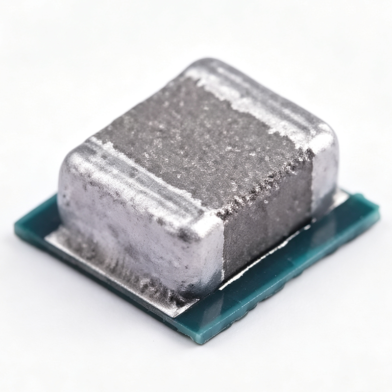
TPS82130SILR - 17V 3A Step-Down MicroSiP Module | TI
The Texas Instruments TPS82130SILR is a compact 17V-input, 3A step-down converter MicroSiP power module that integrates a synchronous buck converter and an inductor into a single 8-pin uSIP (SIL) package measuring 3.0mm x 2.8mm x 1.5mm. It operates from 3V to 17V input and delivers up to 3A continuous output current with an adjustable output from 0.9V to 5V. A step-down converter, also called a buck converter, is a switching DC-DC voltage regulator that converts a higher input voltage to a lower output voltage with high efficiency, forming a core building block of power management IC hierarchies alongside LDOs and power modules. The TPS82130 integrates switching FETs, inductor, and loop compensation into one micro module, dramatically reducing external component count and PCB area compared to discrete regulator designs. Key features include the wide 3V-17V input range supporting 12V and 5V bus systems, 3A output current, adjustable 0.9V-5V output, and a 2.2MHz fixed switching frequency that allows small external capacitors. Efficiency typically exceeds 90% at moderate loads. The module provides a power-good output flag, an enable pin for power sequencing, internal soft-start to limit inrush current, and thermal shutdown protection. Technically, the TPS82130 uses fixed-frequency peak-current-mode control, providing fast transient response and stability with minimal output capacitance. It supports 100% duty cycle operation for low dropout, and the integrated shielded inductor reduces EMI while simplifying layout. The low 1.5mm profile suits automated assembly with standard surface-mount equipment. Typical applications include point-of-load (POL) power for FPGAs, DSPs, and ASICs, industrial sensor supplies, IoT devices, and portable equipment powered from 12V rails. When designing, follow the datasheet recommendations for input and output ceramic capacitance, place the module close to the load, and provide a generous copper area under the thermal pad, especially at high output currents. Pricing references apply as of 2026-08-28.
TPS826711 - 600mA 1.8V MicroSiP Buck Module | Texas Instruments
The Texas Instruments TPS826711 is a fully integrated, low-noise step-down DC-DC converter module in a MicroSiP package, delivering up to 600mA output current. It operates from a 2.3V to 4.8V input and provides a fixed 1.8V output. The module integrates the switching regulator, inductor, and input/output capacitors, requiring no additional external components for a complete power supply solution. This high level of integration minimizes board space and simplifies design, making it ideal for space-constrained portable applications. A step-down converter, also known as a buck converter, is a type of DC-DC converter that steps down an input voltage to a lower output voltage while maintaining high efficiency. It is a fundamental building block in power management, converting a higher voltage rail to a lower one for powering digital ICs, sensors, and other loads. The TPS826711 belongs to the family of switching regulators, which are more efficient than linear regulators for large voltage differences, making them essential in battery-powered devices where power conservation is critical. Key features include a regulated 5.5MHz switching frequency, which allows tiny external components and reduces output ripple. It achieves up to 90% efficiency, minimizing power loss and extending battery life. The device also features a low quiescent current of 17uA, making it suitable for always-on applications. Additionally, it includes spread-spectrum PWM frequency dithering to reduce electromagnetic interference (EMI), a critical feature for noise-sensitive systems. Technically, the TPS826711 is based on a high-frequency synchronous step-down topology, using both high-side and low-side MOSFETs to achieve high efficiency. The integrated inductor and capacitors are co-packaged in the MicroSiP, ensuring predictable performance and reducing parasitic effects. The device operates in power-save mode at light loads, further improving efficiency across the entire load range. Typical applications include powering microcontrollers, DSPs, and other digital ICs in battery-powered devices such as wearables, IoT sensors, and portable medical equipment. Its low noise and high efficiency also make it suitable for RF transceivers and audio codecs where clean power is essential. When designing with the TPS826711, ensure adequate input and output decoupling as recommended in the datasheet. The power-save mode provides excellent light-load efficiency but may introduce output ripple; consider this trade-off in noise-sensitive applications.
TPSM13604H - 4A Step-Down Power Module | Texas Instruments
The Texas Instruments TPSM13604H is a SIMPLE SWITCHER power module that integrates a step-down DC-DC converter with an inductor and other passive components into a compact 7-TO-PMOD package. It accepts an input voltage from 5V to 36V and delivers an adjustable output voltage from 3V to 16V with up to 4A of continuous output current. The module is designed for easy implementation, requiring only three external resistors and four external capacitors to complete the power solution. A power module is a complete DC-DC converter solution that integrates the controller, power FETs, inductor, and often compensation circuitry into a single package. This integration simplifies PCB layout, reduces design time, and improves thermal performance compared to discrete solutions. The TPSM13604H belongs to the SIMPLE SWITCHER family, which is known for its ease of use and robust performance in industrial, automotive, and communications applications. Key features include a wide input voltage range of 5V to 36V, adjustable output voltage down to 3V, and a maximum output current of 4A. The module offers exceptional power conversion efficiency, line and load regulation, and output accuracy. It includes protection features such as thermal shutdown, input undervoltage lockout, output over-voltage protection, short-circuit protection, and output current limit. Additionally, it supports start-up into a pre-biased output and allows the switching frequency to be adjusted up to 700 kHz with a single resistor. The TPSM13604H uses an innovative package that enhances thermal performance and allows for hand or machine soldering. The 7-TO-PMOD package is designed for surface-mount assembly and provides excellent heat dissipation. The module operates over a junction temperature range of -40°C to +125°C, making it suitable for harsh environments. Typical applications include point-of-load (PoL) converters for FPGAs, ASICs, and microprocessors, as well as industrial control systems, test and measurement equipment, and automotive infotainment systems. The wide input range and high output current make it ideal for systems powered from 12V or 24V rails. When designing with the TPSM13604H, ensure proper input and output capacitance to maintain stability and minimize ripple. The adjustable output voltage is set by an external resistor divider, and the switching frequency can be programmed with a single resistor. Adequate thermal management is essential when operating at high output currents and high input-to-output voltage differentials.
TPSM5601R5 - 60V In, 1.5A Step-Down Power Module | TI
The Texas Instruments TPSM5601R5 is a highly integrated 1.5-A step-down DC/DC power module combining a 60-V maximum input converter, power MOSFETs, a shielded inductor, and support passives in a thermally enhanced 5-mm x 5.5-mm x 4-mm 15-pin Enhanced HotRod QFN package. It delivers an adjustable output voltage of 1.0 V to 6 V from a 4.2-V to 60-V input range with a fixed 400-kHz switching frequency. A power module is a complete DC-DC converter solution that integrates the controller, switching MOSFETs, inductor, and compensation network into a single surface-mount package. Within the power management hierarchy (power module -> step-down converter -> DC-DC converter -> power management IC), modules eliminate magnetics selection and loop compensation design, reducing time-to-market and layout risk compared to discrete converter solutions. Key features include the wide 60-V input rating suited to 24-V and 48-V industrial rails with transient headroom, an output range of 1.0 V to 6 V set by a single external resistor divider, and as few as four external components for the complete solution. The Enhanced HotRod QFN construction places the die directly against the thermal pad, delivering low EMI, excellent thermal performance, and all pins accessible from the package perimeter for simple layout and inspection. The internal compensation and integrated shielded inductor provide stable operation across the load range while reducing solution height and BOM count. The device operates from a -40C to +125C junction temperature range, supporting industrial and automotive-adjacent environments. The TPSM5601R5S variant adds spread-spectrum operation for lower EMI peaks, and the TPSM5601R5H variant extends output capability up to 16 V. Typical applications include 24-V and 48-V industrial bus power supplies, factory automation and PLC I/O modules, test and measurement point-of-load rails, and distributed power systems that need a compact, regulated 1-V to 6-V rail from a wide input. Design tip: because the inductor is integrated, thermal design centers on the PCB copper pour under the thermal pad - provide at least a 1-square-inch ground plane with thermal vias for reliable operation at full 1.5-A load at elevated ambient temperatures.
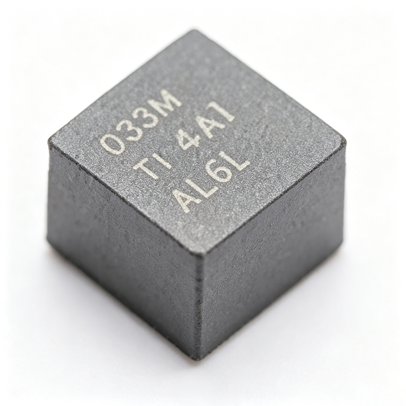
TPSM81033VCDR - 2A 2.4MHz Synchronous Boost Module | TI
The Texas Instruments TPSM81033VCDR is a 5.5V, 2A synchronous boost power module using TI MagPack packaging technology, integrating a 0.43uH power inductor, power MOSFETs, and control circuitry into a 2.6mm x 2.5mm QFN-FCMOD (9) package. It accepts 1.8V to 5.5V input and delivers a 2.2V to 5.5V output with a 2A typical valley switching current limit. A boost converter (step-up switching regulator) is a DC-DC converter that raises an input voltage to a higher regulated output by storing energy in an inductor and releasing it at higher voltage through a switching FET. Boost converters form part of the power management IC hierarchy and are essential wherever battery voltage is lower than the load rail, such as single-cell Li-ion or alkaline systems needing a 5V rail. Key features include the integrated inductor enabled by MagPack technology, 2.4MHz switching frequency that allows tiny external components and fast transient response, fixed 5.0V output option by connecting FB to AVIN, selectable light-load mode (auto PFM or forced PWM) via the MODE pin, and power-good output. Protection features include 5.75V output overvoltage protection, output short-circuit protection, and thermal shutdown. The device uses adaptive constant on-time valley-current-control topology, providing fast load transients and predictable behavior. Forced PWM mode trades light-load efficiency for constant switching frequency, important for noise-sensitive RF and analog rails. Typical applications include smart devices and portable battery-powered equipment, RF power amplifiers needing a stable 5V from Li-ion cells, and OLED or display bias supplies. The tiny footprint and minimum external component count make it ideal for space-constrained wearables and IoT devices. Design consideration: boost converter output current capability decreases as input voltage drops; verify the 2A valley current limit supports your load at minimum VIN, and follow the datasheet PCB layout for thermal performance of the exposed package.
TPSM81033VCDR - 2A, 2.4MHz Boost Power Module | TI
The Texas Instruments TPSM81033VCDR is a 5.5V, 2A, 2.4MHz synchronous boost power module using MagPack packaging technology. It integrates a 0.43uH power inductor, power switches, and control circuitry into a compact 2.6mm x 2.5mm QFN-FCMOD (9) package, providing a nearly complete DC-DC boost converter solution with a minimum of external components. A power module is a type of DC-DC converter that integrates the power inductor and MOSFETs of a switching regulator into a single surface-mount package, sitting within the broader hierarchy of power management ICs that also includes LDOs, buck converters, and controllers. By integrating magnetics, modules dramatically reduce solution size and simplify layout compared to discrete converter designs. Key features include a 1.8V to 5.5V input voltage range, an adjustable 2.2V to 5.5V output voltage range (with fixed 5.0V output when FB is connected to AVIN), a 2A valley switching current limit, and integrated 0.43uH power inductor with excellent thermal performance. The device operates at 2.4MHz switching frequency using an adaptive constant on-time valley-current-control topology, enabling small external components and fast transient response. The module offers two light-load modes selected via the MODE pin: automatic PFM mode for highest efficiency and forced PWM mode for fixed-frequency noise immunity. Protection features include 5.75V output overvoltage protection, output short-circuit protection, and thermal shutdown. A power good output supports power-rail monitoring and sequencing. Typical applications include battery-powered smart devices, portable equipment, Li-ion cell to 5V conversion, and point-of-load boost rails in compact electronics where board space is constrained. The small 2.6mm x 2.5mm footprint suits wearables and handheld instrumentation. Design consideration: because the current limit is a valley limit of 2A typical, verify peak inductor current under worst-case load, minimum input voltage, and maximum output power to avoid hitting current limit during load transients.
TPSM81033VCDR - 5.5V 2A Boost Power Module | Texas Instruments
The Texas Instruments TPSM81033VCDR is a 5.5V, 2A synchronous boost power module with MagPack packaging technology, integrating a 0.43uH power inductor and power MOSFETs in a compact 2.6mm x 2.5mm QFN-FCMOD (9) package. It operates from a 1.8V to 5.5V input and delivers an adjustable 2.2V to 5.5V output, with a fixed 5.0V option by connecting FB to AVIN. A boost converter is a DC-DC switching regulator that steps an input voltage up to a higher output voltage. It is essential in battery-powered systems where cell voltage falls below the required rail. The TPSM81033 belongs to the power module family within power management ICs, integrating the magnetic component and power stage to reduce design effort and board space versus discrete solutions. Key features include a 2A valley switching current limit, fixed 2.4MHz switching frequency for small external components and low ripple, and an integrated 0.43uH inductor with excellent thermal performance. Adaptive constant on-time valley-current-control topology regulates the output, while two light-load modes (auto PFM and forced PWM) selected via the MODE pin balance efficiency and noise immunity. Optional spread spectrum frequency modulation minimizes EMI. The synchronous rectifier architecture eliminates the external Schottky diode, improving efficiency, and the integrated inductor reduces parasitic losses and radiated EMI. Only input and output capacitors plus feedback resistors are required. Protection features include 5.75V output overvoltage protection, output short-circuit protection, thermal shutdown, and a power good output for sequencing in multi-rail systems. Typical applications include smart devices and portable equipment powered by batteries, IoT sensor power supplies, and TFT-LCD bias or OLED display rails. The wide input range and high switching frequency suit space-constrained designs. Design tip: ensure adequate input and output capacitance for stability and low ripple, and use the MODE pin to trade efficiency against noise. For a fixed 5V output, tie FB to AVIN per the datasheet layout guidelines.
TPSM82813 - 3A 6V Step-Down Power Module | TI
The Texas Instruments TPSM82813 is a synchronous step-down DC/DC power module with integrated inductor, delivering up to 3A output current from a 2.75V to 6V input supply. Available in QFN and MagPack (SIL) packages, output voltage is adjustable from 0.6V to 5.5V via external resistors. A step-down (buck) converter is a DC/DC power converter that efficiently reduces a higher input voltage to a lower regulated output. Power modules integrate the inductor and control circuitry into a single package, sitting one level above discrete buck converters in the power management IC hierarchy and dramatically reducing design effort and PCB area compared to controller-plus-inductor solutions. Key features include optional frequency synchronization, adjustable soft-start, and output voltage tracking for power sequencing. The device also offers spread spectrum for EMI reduction, a power good output, adjustable UVLO, and light-load efficiency mode. Efficiency reaches approximately 95%, minimizing losses in high-current point-of-load designs. Technically, the TPSM82813 uses a fixed-frequency peak current-mode control topology, providing fast transient response and stable loop behavior. The integrated inductor is optimized for low loss and contained EMI, while the MagPack package improves thermal performance. Thermal behavior is characterized on a JEDEC 51-7 defined PCB. Typical applications include point-of-load converters for FPGAs, DSPs, and ASICs, plus power supplies for telecommunication, test and measurement, medical, and industrial sensor equipment. The wide 2.75V-6V input supports 5V and 3.3V bus conversions, and the small footprint enables dense rail designs. Design tip: follow datasheet input/output capacitance recommendations, configure soft-start and tracking for your power-up sequence, and use thermal vias under the module per the recommended land pattern. Pricing as of 2026-08-30, see tiers below.
TPSM82816 - 6A Step-Down Power Module 2.7-6V | TI
The Texas Instruments TPSM82816 is a 2.7V to 6V input, 6A output synchronous step-down DC/DC power module with an integrated inductor, packaged in the compact MicroSiP (SIE) package. It belongs to the TPSM8281x family of pin-to-pin 1A, 2A, 3A, 4A, and 6A compatible modules, delivering high power density and ease of use for point-of-load (PoL) power supplies. A step-down power module is a complete DC/DC converter solution that combines the switching regulator, power MOSFETs, and magnetic components in a single package. Unlike discrete regulators that require separate inductor selection and layout optimization, power modules simplify design, shrink solution size, and reduce EMI and efficiency risk. Power modules sit within the power management IC hierarchy, bridging discrete converters and fully integrated PMICs. Key features include an adjustable output voltage from 0.6V to 5.5V via a single resistor divider, optional frequency synchronization to an external clock, adjustable soft-start, and output voltage tracking for rail sequencing. Peak efficiency exceeds 90% for typical 5V-to-1.8V conversions, with the shielded integrated inductor improving EMI behavior. The device is based on a fixed-frequency peak current-mode control topology, which provides fast transient response and stable operation with ceramic output capacitors. The package integrates everything needed for a minimal-footprint POL supply, and protection features include overcurrent, overvoltage, and thermal shutdown. The switching frequency can be programmed to trade efficiency against solution size. Typical applications include POL power for FPGAs, ASICs, and processors in telecommunication, test and measurement, medical, and industrial systems, where TI cites high power density and ease of use as primary benefits. Because the family is pin-to-pin compatible, a single PCB layout supports current tiers from 1A to 6A, simplifying BOM scaling across product variants. When designing with the TPSM82816, provide adequate input and output ceramic capacitance for stability and transient response, and use the SS/TRACK pin to sequence multiple rails in multi-voltage systems.
TPSM82822A - 2A Step-Down Module, Integrated Inductor | TI
The Texas Instruments TPSM82822A is a 5.5-V input, 2-A synchronous step-down converter power module with an integrated inductor and forced PWM mode, housed in a compact 2 x 2.5 x 1.1 mm MicroSiP (uSiP) package. It delivers an adjustable output from 0.6 V to 4 V, simplifying point-of-load power design. A step-down converter, or buck converter, is a switching voltage regulator that efficiently reduces a higher DC input voltage to a lower regulated output. Within the power management IC hierarchy, the TPSM82822A is a power module: it integrates the buck converter IC, power MOSFETs, and the magnetic inductor into one surface-mount package, collapsing an entire DC-DC solution into about 5 mm2 of board area. Key features include a 2.4 V to 5.5 V input range, 2 A continuous output current, forced PWM operation for constant 2.2 MHz switching frequency and predictable EMI, power-good output, enable pin, and internal soft-start. Efficiency reaches approximately 95% at typical loads, and the high operating frequency allows small external capacitors and low output ripple. Technically, the module uses a synchronous buck architecture with integrated low-DS(on) MOSFETs and a proprietary control scheme. Integrating the inductor inside the package minimizes parasitic loop inductance, reduces radiated EMI, and enables automated assembly with standard surface-mount equipment per the TPSM8282x datasheet. Typical applications include powering FPGAs, DSPs, ASICs, and MCUs in industrial systems, optical modules, solid-state drives, and portable devices where board space is at a premium. Forced PWM keeps output ripple low and constant-frequency, suiting noise-sensitive analog and RF rails. Design consideration: follow the datasheet input/output capacitor recommendations exactly for stability, and provide adequate thermal copper area for sustained 2 A loads; the module does not eliminate thermal design entirely.
TPSM828303 - 3A Low-EMI Buck Module 2.25-5.5V | Texas Instruments
The Texas Instruments TPSM828303 is a 3A synchronous step-down DC/DC power module with integrated inductor, operating from a 2.25V to 5.5V input and providing an adjustable output from 0.5V to 4.5V in a compact QFN (RDS) or MagPack (PVC) package. A DC/DC power module is a complete point-of-load power supply that integrates the controller, power MOSFETs, inductor, and compensation into a single surface-mount package. As a member of the buck (step-down) converter family within the broader power management IC hierarchy, it efficiently reduces a higher input voltage to a lower output voltage while minimizing external component count, layout effort, and design risk compared to discrete converter solutions. Key features include the DCS-Control topology for fast load transient response with small output capacitance, 1% feedback voltage accuracy over the full operating range, and integrated EMI reduction technologies that ease radiated emissions compliance. Automatic PWM/PFM transition maximizes light-load efficiency, and enable, power good, output discharge, and overcurrent protection functions simplify system integration. The TPSM828303 is pin-to-pin compatible with the 1A (TPSM828301) and 2A (TPSM828302) family members, enabling current-rating scalability on one PCB layout. The integrated inductor with MagPack magnetic shielding (TPSM828303APVCBR variant) reduces radiated EMI and board area versus discrete designs. Operation over a -40C to +125C junction range suits industrial environments. Typical applications include point-of-load (POL) power for FPGAs, DSPs, and ASICs, optical module supplies, test and measurement equipment, and noise-sensitive portable designs where low EMI is mandatory. Design tip: follow the datasheet input/output capacitance recommendations - the DCS-Control topology supports output capacitors up to 200uF, and the EN pin plus power good signal enable proper rail sequencing in multi-rail systems. Prices as of 2026-08-30.
TPSM82866A - 6A Step-Down Power Module | Texas Instruments
The Texas Instruments TPSM82866A is a 6A step-down power module with an integrated inductor, operating from a 2.4V to 5.5V input and providing an adjustable output from 0.6V to 5.5V. It comes in a 3.5mm x 4.0mm thin overmolded QFN package (RDJ), integrating a synchronous buck converter and shielded inductor for a compact point-of-load solution. A step-down power module is a complete DC-DC converter solution that integrates the controller, power FETs, and inductor into a single package. Belonging to the power management IC family of non-isolated point-of-load (PoL) converters, such modules reduce design complexity, minimize PCB area, and improve thermal performance compared to discrete buck converter designs, which is essential for powering modern digital loads. Key features include 6A continuous output current, high efficiency, and DCS-Control topology for fast transient response and stable operation. The integrated 220nH shielded inductor (±20% tolerance in RDJ/RDM packages) provides excellent EMI performance. The module offers power-good output, enable pin, and adjustable switching frequency for flexible power sequencing and design optimization. Technically, the TPSM8286xA family uses the DCS-Control (Direct Control with Seamless transition into energy saving mode) architecture, delivering fixed-frequency operation with excellent load and line regulation. The TPSM82864A and TPSM82866A in RDJ and RDM packages are pin-to-pin and BOM-to-BOM compatible, allowing a 4A option on the same footprint. The TPSM8286xAA0HRDMR variants provide higher efficiency due to increased package height, and the RCF MagPack variant uses a 200nH inductor with enhanced EMI shielding. Typical applications include core power supplies for FPGAs, CPUs, and ASICs, optical modules, and medical and industrial equipment, where board space is at a premium and high current density is required. When designing with this module, ensure adequate input and output capacitance for stability. The integrated inductor simplifies layout, but proper grounding and thermal vias remain essential for optimal thermal performance at full 6A load.
TPSM82866C - 6A Step-Down Power Module I2C | Texas Instruments
The Texas Instruments TPSM82866C is a 6A step-down power module with an integrated inductor and I2C interface, designed for compact, high-density power delivery. It operates from a 2.4V to 5.5V input and provides an adjustable output voltage, making it suitable for a wide range of point-of-load (PoL) applications. The module is housed in a MagPack (RCF) QFN package measuring only 2.3mm x 3mm, achieving a power density of nearly 1A per 1mm2 of area. A step-down power module is a complete DC-DC converter that integrates the controller, power FETs, inductor, and compensation into a single package. This integration simplifies design, reduces external component count, and minimizes PCB footprint compared to discrete buck regulator solutions. The TPSM82866C belongs to the TPSM8286xx family, which includes 4A (TPSM82864x) and 6A (TPSM82866x) variants, all pin-to-pin and BOM-to-BOM compatible, allowing easy scalability between current ratings. Key features include a 200nH shielded inductor that enhances EMI performance, an I2C interface for dynamic voltage scaling and telemetry, and high efficiency across the load range. The module supports output voltage programming via I2C or external resistors, and includes soft-start, overcurrent protection, and thermal shutdown. The RCF MagPack package shields both the inductor and the IC, further improving EMI performance. The TPSM82866C uses a synchronous buck topology with integrated MOSFETs, achieving high efficiency at light and full loads. The I2C interface allows real-time monitoring of output voltage, current, and temperature, enabling adaptive power management. The integrated, shielded inductor reduces EMI and simplifies layout. Typical applications include FPGA, ASIC, and DSP power supplies, server and networking equipment, and industrial automation. The I2C interface is particularly useful in systems requiring dynamic voltage scaling or telemetry. When designing with this module, ensure proper input and output capacitance for stability and transient response. Configure the I2C address and output voltage settings per system requirements, and provide adequate PCB copper area for heat dissipation.
TUHS3F12 - 3W 12V 250mA PCB Mount AC-DC Converter | Cosel
The Cosel TUHS3F12 is a 3 W PCB-mount enclosed AC-DC converter module delivering a single regulated 12 V output at 250 mA, with a universal input range of 85 to 264 VAC (50/60 Hz) or 120 to 370 VDC. The module belongs to Cosel's TUHS series of compact board-mount power supplies designed for direct installation onto a printed circuit board without an external enclosure. An AC-DC converter (also called an off-line power supply module) converts mains alternating current into a low-voltage regulated direct-current output. Within the power-management hierarchy, it sits above DC-DC converters, which only convert an already-rectified DC rail; an AC-DC module handles rectification, power-factor correction, isolation, regulation, and protection in a single encapsulated package. Key features of the TUHS3F12 include built-in overcurrent and overvoltage protection circuits, a small footprint that greatly reduces board area, and design flexibility for hold-up time and expected life. Cosel's series documentation highlights low-noise technology and soft switching circuits that achieve high efficiency and low standby power across the TUHS range (3 W to 30 W). Notably, the module is not built with aluminum or tantalum electrolytic capacitors, which improves long-term reliability and extends expected service life compared with conventional designs. Technically, the TUHS3F12 is a member of the 3 W tier of the TUHS family; larger family members such as the TUHS25 employ synchronous rectification for further efficiency gains. The universal input permits direct connection to worldwide single-phase mains without jumper selection, making the module suitable for globally deployed equipment. The encapsulated through-hole construction provides resistance to dust, moisture, and vibration. Typical applications include industrial control equipment, household appliances, network and communication devices, LED lighting drivers, and instrumentation where a compact, isolated low-power auxiliary supply is required directly on the main PCB. A key design consideration is thermal derating: at 3 W output the module must be mounted with adequate airflow and spacing to keep case temperature within the datasheet limit, and output current should not exceed 250 mA continuously. Hold-up time can be extended with an external output capacitor per Cosel's application guidance. This page synthesizes distributor pricing, drop-in family alternatives, and practical design notes not found in the manufacturer datasheet.

UC3824 - 1.5A High Speed PWM Controller | Texas Instruments
The Texas Instruments UC3824 is a high-speed, double-ended PWM controller designed for switch-mode power supplies requiring operating frequencies up to 1 MHz. It integrates a 30-V, 1.5-A totem-pole output stage capable of driving power MOSFETs directly, along with a 9.2-V/8.4-V undervoltage lockout (UVLO) and a maximum duty cycle of 85%. The device is available in a 16-pin PDIP package (UC3824N) and operates over the commercial temperature range of 0°C to 70°C. A PWM controller is an integrated circuit that generates the pulse-width-modulated signals used to control the switching elements in a DC-DC converter or power supply. It forms the core of the control loop, regulating output voltage or current by varying the duty cycle of the switching waveform. The UC3824 belongs to the family of current-mode PWM controllers, which offer superior line regulation and simpler compensation compared to voltage-mode controllers. In the hierarchy of power management, it sits between the power stage (MOSFETs, transformers) and the supervisory circuitry, providing the precise timing and drive signals essential for efficient power conversion. Key features of the UC3824 include a 50-ns propagation delay to output, enabling high-frequency operation with minimal phase lag. The dual totem-pole outputs can source and sink 1.5 A, providing robust gate drive for large MOSFETs. The device also includes a current-limit comparator with a 1-V threshold, a TTL-compatible shutdown port, and a soft-start pin that doubles as a maximum duty cycle clamp. The logic is fully latched to ensure jitter-free operation and prevent multiple pulses at the output. Technically, the UC3824 uses a fixed-frequency, current-mode architecture with an internal oscillator whose frequency is set by external timing components RT and CT. The ramp generator is designed so that the voltage at Pin 9 crosses the 1-V threshold at the same time the desired maximum volt-second product is reached, allowing precise control of the duty cycle. The device's high-speed comparator and latch ensure accurate cycle-by-cycle current limiting, making it suitable for demanding applications such as push-pull and half-bridge converters. Typical applications include switch-mode power supplies for telecommunications, industrial power converters, and battery chargers. The UC3824's high-frequency capability allows for smaller magnetic components, reducing overall system size and cost. Its double-ended output configuration makes it ideal for push-pull and full-bridge topologies where two interleaved drive signals are required. When designing with the UC3824, careful attention must be paid to grounding and bypassing, as the high-speed switching can introduce noise. A ground plane is highly recommended, and the timing components should be placed close to the IC to minimize parasitic inductance. The soft-start pin should be used to limit inrush current during startup, and the current-limit threshold should be set appropriately for the application.
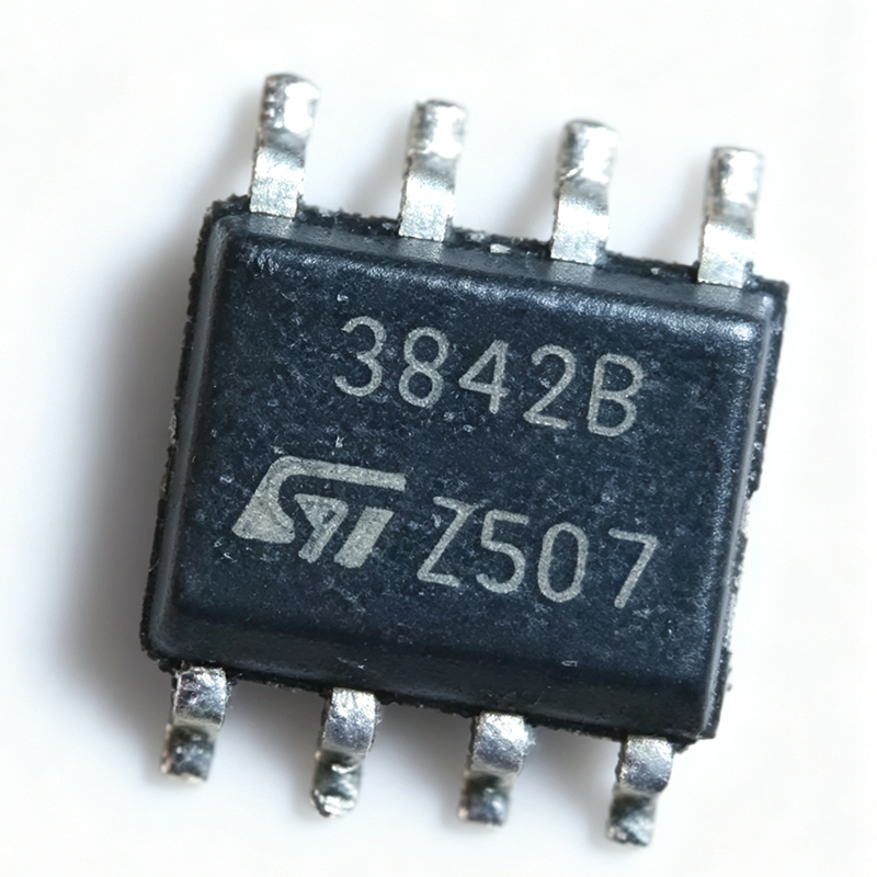
UC3842BD1 - Current Mode PWM Controller | STMicroelectronics | SMPS
The STMicroelectronics UC3842BD1 is a high-performance current-mode PWM controller designed for off-line and DC-to-DC converter applications. It operates with an input voltage range of 7.5V to 30V and provides a 1A peak output current for driving power MOSFETs. The device is available in an SOIC-8 package, making it suitable for compact power supply designs. A current-mode PWM controller is a type of switching regulator control IC that regulates output voltage by comparing the output error signal with a current-sense signal from the power switch. This architecture provides inherent feed-forward compensation, cycle-by-cycle current limiting, and simplified loop compensation compared to voltage-mode controllers. The UC3842BD1 belongs to the UC3842 family of PWM controllers, which are widely used in AC-DC adapters, battery chargers, and industrial power supplies. Key features of the UC3842BD1 include a trimmed oscillator for precise frequency control, an under-voltage lockout (UVLO) with hysteresis, a 5V reference output, and a high-gain error amplifier. The oscillator frequency is programmable up to 500 kHz, allowing designers to optimize transformer size and efficiency. The device also features a low startup current of 0.5 mA, which is critical for efficient power-up in battery-powered systems. The UC3842BD1 uses a fixed-frequency current-mode architecture with a maximum duty cycle of 96%. The error amplifier has a bandwidth of 1 MHz, enabling fast transient response. The current-sense comparator has a threshold of 1V, providing accurate cycle-by-cycle current limiting. The device is designed to operate over a junction temperature range of -40°C to +150°C, ensuring reliability in harsh environments. Typical applications include switch-mode power supplies (SMPS) for consumer electronics, industrial power converters, and battery chargers. The UC3842BD1 is also used in flyback and boost converter topologies, where its current-mode control simplifies loop compensation and improves line regulation. When designing with the UC3842BD1, ensure that the current-sense resistor is placed close to the IC to minimize parasitic inductance. The oscillator timing resistor and capacitor should be located near the RT/CT pin to reduce noise coupling. Proper grounding and decoupling of the VCC pin are essential for stable operation. This page synthesizes distributor pricing, drop-in alternatives, and practical design notes not found in the STMicroelectronics datasheet, providing engineers with a comprehensive resource for selecting and implementing the UC3842BD1.