Interface ICs
Subcategories
Products (3,400+)

PCI4451GJG - Integrated PC Card & 1394 OHCI Controller | TI
The Texas Instruments PCI4451GJG is an integrated PC Card controller and 1394 (FireWire) OHCI controller that combines dual-slot CardBus (PCMCIA) support with a single 400 Mbps IEEE 1394a link in a single PCI device. It supports two independent PC Card slots compliant with the 1997 PC Card Standard, provides a 32-bit CardBus bridge for both slots, and integrates a 3.3 V physical layer for IEEE 1394 with one fully compliant cable port at 100/200/400 Mbps. The device is offered in a 257-ball MicroStar BGA (GJG) package, 16x16 mm, designed for space-constrained add-in cards and embedded platforms. Key features include PCI 2.2 host-side compliance, integrated 1394 OHCI 1.1 controller with cable power management, support for Zoom Video (ZV) port, ACPI 1.0 compliant power management with D0/D1/D2/D3 states and PME#, and programmable CardBus signal voltage (3.3 V / 5 V / VPP). The integrated PHY removes the need for an external 1394 link-layer chip, reducing both BOM count and PCB area versus two-chip implementations. Technically, the PCI4451 uses a single 33 MHz, 32-bit PCI bus to bridge the host CPU to two PC Card sockets and one 1394 port. Internal DMA engines handle PC Card data movement with scatter-gather support, while a dedicated 1394 PHY implements bus-reset, arbitration, and cable-not-active detection per IEEE 1394a-2000. CardBus card insertion/removal is managed by per-socket card detect and voltage sense pins that feed the integrated socket controller. Typical applications include legacy industrial PCs, test and measurement chassis with PC Card (PCMCIA) data acquisition modules, docking stations, embedded military/aerospace single-board computers, and add-in Combo cards (CardBus + 1394a) for legacy Windows XP / Windows 2000 platforms where both buses remain in active service for instrumentation capture. When designing, observe the 257-ball BGA escape pattern: route CardBus data, address and control signals on the outer two rows of balls and place the 1394 cable port traces near the package edge to minimize stub length. A 27 MHz crystal with the on-chip PLL provides the 1394 PHY clock; follow TI's reference layout for the PHY section to remain IEEE 1394a compliant. This page synthesizes distributor pricing, exact-package alternatives, and practical design notes not found in the manufacturer datasheet alone.
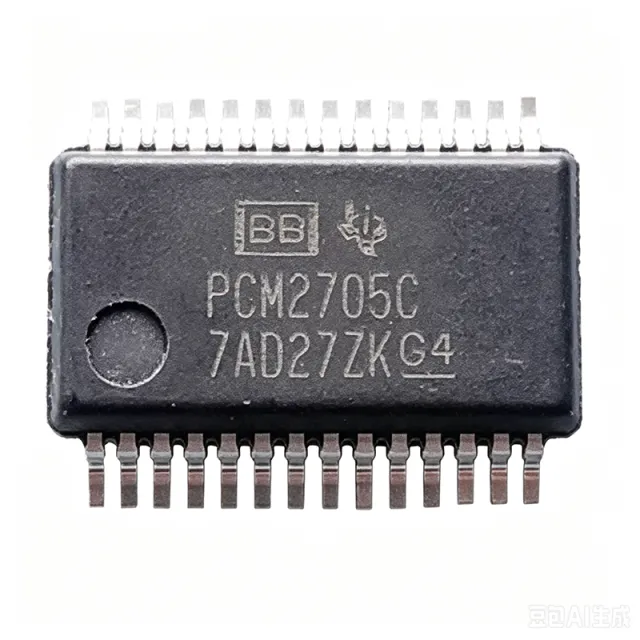
PCM2705C - 98dB SNR Stereo USB DAC with S/PDIF | Texas Instruments
The Texas Instruments PCM2705C is a single-chip stereo audio digital-to-analog converter (DAC) with an integrated USB 2.0 full-speed protocol controller and S/PDIF output. It delivers 98dB SNR and supports both bus-powered and self-powered operation with software control. The device is fully compliant with USB 2.0 specifications and USB Audio Class, requiring no dedicated device driver. It comes in a 28-pin SSOP package, making it ideal for compact audio applications. A USB audio DAC is a digital-to-analog converter that receives digital audio data from a USB host and converts it to analog audio signals. It integrates the USB interface, protocol controller, and DAC core into a single chip, simplifying system design. The PCM2705C sits in the hierarchy of audio converters, specifically as a USB audio interface IC, which is a subset of audio data converters within the broader category of mixed-signal ICs. Key features include a 98dB SNR stereo DAC, S/PDIF output, and support for both bus-powered and self-powered modes. The device also features partially programmable USB descriptors, allowing customization of vendor ID and product ID via an external SPI host. The integrated USB transceiver eliminates the need for external PHY, reducing BOM cost and board space. Technically, the PCM2705C uses adaptive isochronous transfer for audio data, ensuring synchronized playback. The S/PDIF output supports digital audio transmission to external decoders or amplifiers. The device operates from a 3.3V supply and includes an internal PLL for clock generation, minimizing external components. The SSOP-28 package provides a compact footprint suitable for portable and space-constrained designs. Typical applications include USB sound cards, docking stations, gaming headsets, and portable audio interfaces. The device's plug-and-play capability makes it ideal for consumer audio products where driver installation is undesirable. Its low power consumption and small size also suit battery-powered devices. When designing with the PCM2705C, ensure proper decoupling of the 3.3V supply and careful layout of the USB differential pair to maintain signal integrity. The SPI interface for descriptor programming should be configured during initial setup, and the PSEL and HOST pins must be set correctly for the desired operating mode.

PCM3000E - 18-Bit Stereo Audio Codec | Texas Instruments
The Texas Instruments PCM3000E is an 18-bit stereo audio codec with integrated analog-to-digital and digital-to-analog converters, 64-times oversampling, and a 28-pin SSOP package. It accepts single-ended analog voltage inputs and produces single-ended analog voltage outputs, combining stereo recording and playback functions in one low-cost CMOS device. An audio codec is a mixed-signal interface IC that converts between digital audio data and analog voltage signals. In the signal-chain hierarchy, the PCM3000E sits between an audio signal source or microphone front end and a digital audio processor, microphone preamplifier, and analog output amplifier. Its ADC path digitizes stereo analog inputs, while its DAC path reconstructs stereo audio from serial digital data. The integrated converters make it useful in cost-sensitive consumer equipment requiring more functionality than a basic interface controller. Key features include 18-bit ADC and DAC resolution, stereo operation, single-ended analog inputs and outputs, and 64-times ADC oversampling. The DAC section uses an 8-times oversampling digital interpolation filter. A serial interface provides a straightforward connection to digital audio processors, while the integrated codec architecture reduces the number of separate converters required in a stereo audio subsystem. The PCM3000E uses delta-sigma modulation for both conversion paths. Delta-sigma ADCs oversample the analog input and use digital decimation filtering, while the DAC path combines digital interpolation filtering with a single-bit delta-sigma conversion stage. This architecture supports compact, cost-sensitive stereo audio designs and is suited to consumer applications where good performance is required without the complexity of a high-resolution multibit converter. Typical uses include consumer digital audio equipment, portable audio products, stereo cassette and CD-style playback systems, and other sound-processing products. It can also support multichannel designs when multiple codec channels are combined. For digital signal processing, the codec can work with serial audio processors, microcontrollers, or DSPs capable of handling the required master clock, serial data, and control signals. Designers should follow the pin-description table in the manufacturer datasheet when assigning signal paths and decoupling. The analog supply, digital supply, clock, serial interface, and analog-output circuitry require careful partitioning to prevent switching activity and digital coupling from degrading audio performance. The 28-pin SSOP package is compact but has a relatively narrow lead pitch, so PCB assembly and inspection require suitable fine-pitch capability. This page organizes the PCM3000E specifications, pin and package information, product comparisons, engineering guidance, and available drop-in alternatives for faster design review. It also identifies lifecycle and sourcing considerations that should be checked before committing to a new production design.

PCM3002E - Low-Power Stereo Audio Codec | Texas Instruments
The Texas Instruments PCM3002E is a low-power stereo audio codec with 16/20-bit resolution, two analog inputs, two analog outputs, and a 24-pin SSOP package. It combines delta-sigma ADCs and DACs with a 20-bit serial audio interface and software-controlled line output, making it suitable for cost-sensitive consumer audio equipment. A stereo audio codec is a mixed-signal semiconductor that converts two analog audio channels into digital data and converts digital audio data back into two analog output channels. In the signal-chain hierarchy, PCM3002E belongs to the audio codec category, combines analog-to-digital converters and digital-to-analog converters, and ultimately supports digital signal processing and audio playback systems. The converter architecture uses delta-sigma modulation with 64-times oversampling. According to the Texas Instruments product information, the ADCs include a digital decimation filter, while the DACs use an 8-times oversampling digital interpolation filter. The 16/20-bit interface supports digital audio formats identified in the family documentation as I2S, L, right-justified I2S, and L/R formats, allowing the device to interface with common audio processors and digital audio buses. The PCM3002 and PCM3003 family is manufactured using an advanced CMOS process and is positioned for cost-sensitive consumer applications where audio performance and low power consumption are important. The 24-pin SSOP package provides a compact surface-mount implementation for consumer audio boards, and the software-controlled line output provides an additional output-control option for system integration. Typical applications include consumer stereo audio systems, portable media equipment, compact digital amplifiers, USB or portable audio accessories, television audio subsystems, and embedded audio interfaces. In each case, the device consolidates two ADCs, two DACs, filtering, and the digital serial interface into one package, reducing the number of separate converter components required on the printed circuit board. When designing a PCB around the PCM3002E, use the manufacturer pin-description table and layout guidance to assign every signal, supply, ground, and reference connection. Decoupling should follow the datasheet recommendations, analog and digital return paths should be routed carefully, and unused inputs should be configured according to the application circuit rather than left electrically unterminated by assumption. This product page combines the device architecture, package information, practical application guidance, sourcing options, and verified equivalent references to support faster component selection and board-level design. It also highlights where an exact replacement is available and when a proposed substitute requires additional engineering verification.
PCM3003E - Low-Power Stereo Audio Codec | Texas Instruments
Texas Instruments PCM3003E is a low-power stereo audio codec with 16-bit or 20-bit resolution, single-ended analog inputs and outputs, and a 24-pin SSOP package. The device operates from a 2.7 V to 3.6 V analog supply and supports an industrial temperature range of -25 °C to +85 °C. An audio codec is an integrated interface that converts between analog audio signals and digital PCM data. The PCM3003E combines stereo analog-to-digital and digital-to-analog conversion functions in one IC, making it suitable for compact consumer audio equipment where component count, power consumption, and board area are important. Its digital audio interface and analog signal path support equipment such as consumer audio systems, portable products, and compact multimedia devices. The PCM3003E offers selectable 16-bit or 20-bit operation, providing flexibility for designs that balance conversion resolution against system data rate and storage requirements. Its line output includes hardware control, allowing the output stage to be managed according to the product architecture. A single-ended analog interface can simplify PCB routing, although grounding and signal-return design remain important for low-noise performance. The codec is manufactured using an advanced CMOS process and is intended for cost-sensitive consumer applications that require good audio performance without a high-complexity audio interface. The 24-pin SSOP package supports conventional surface-mount assembly and is compatible with automated production processes. System designers should follow the manufacturer pin-description table and recommended application circuit when assigning PCB tracks. Typical PCM3003E applications include stereo audio playback and capture, consumer media equipment, compact sound systems, and embedded audio products. The 2.7 V to 3.6 V operating range supports low-voltage digital platforms, while the -25 °C to +85 °C temperature range covers industrial environments. External decoupling, controlled analog grounding, and careful clock routing should be treated as core parts of the analog design. This product page combines manufacturer specifications, packaging information, application guidance, and engineering comparisons. It also distinguishes the PCM3003E from identified family variants and highlights the design checks that matter when integrating a low-power stereo codec into a mixed-signal PCB.
PCM3006T - 16-Bit Stereo Audio Codec | Texas Instruments
Texas Instruments PCM3006T is a low-cost, single-chip stereo audio codec with 16-bit resolution, single-ended analog inputs and outputs, and a 24-SSOP package. The codec combines analog-to-digital and digital-to-analog conversion functions on one device, reducing the component count in stereo audio equipment. Its delta-sigma conversion architecture uses 64-times oversampling, while the ADC path includes a digital decimation filter for converting the oversampled stream into the required audio-rate data. An audio codec is a mixed-signal interface IC that bridges an analog audio system and a digital audio processor. In this product hierarchy, the PCM3006T is a stereo audio codec, which combines an ADC, DAC, analog input and output circuitry, and digital audio data interfaces. It is used where a system needs bidirectional conversion between analog audio signals and a serial digital audio bus rather than a complete USB audio interface or loudspeaker amplifier. The principal functional attributes of the PCM3006T include 16-bit stereo conversion, single-ended analog input and output, 64-times delta-sigma oversampling, and a digital decimation filter in the ADC path. These features make it suitable for compact stereo audio products in which an existing digital audio engine must interface directly with analog microphones, line-level circuitry, speakers, or other analog audio stages. The integrated codec architecture also helps reduce board area compared with separate ADC and DAC devices. The 24-SSOP package is intended for surface-mount assembly and provides a compact implementation for audio equipment. Because the codec performs both conversion directions, board layout should keep the analog input, analog output, digital interface, and supply connections arranged to minimize coupling between sensitive audio nodes and high-speed digital signals. External analog filtering, grounding, and supply-decoupling decisions remain part of the complete signal-chain design rather than being determined solely by the codec specifications. Typical applications include stereo sound-card analog sections, portable audio products, digital mixing consoles, audio-recording interfaces, speaker and headphone subsystems, and embedded equipment that already has a separate USB or digital audio controller. The PCM3006T is particularly appropriate where single-ended analog connections are acceptable and a 16-bit stereo serial interface is sufficient. It does not itself perform USB connectivity or drive a loudspeaker directly, so those functions require suitable companion circuitry. Designers should verify the complete pin configuration, supported digital audio format, sampling-rate range, analog signal limits, and power requirements in the manufacturer datasheet before layout release. The single-ended interface simplifies some analog routing, but it may reduce headroom or flexibility compared with a codec that offers balanced inputs and outputs. Appropriate passive networks, stable references, clean supplies, and controlled return paths remain essential for low distortion and acceptable channel matching. This product summary combines the verified 16-bit stereo codec identity, single-ended analog I/O, 64-times oversampling, digital decimation, and 24-SSOP packaging information with practical selection guidance, comparison notes, sourcing workflow, and design-focused considerations.

PCM3060PW - 24-Bit Stereo Audio Codec | Texas Instruments
Texas Instruments PCM3060PW is a single-chip 24-bit stereo audio codec with two single-ended analog inputs, two differential analog outputs, 16–96 kHz sampling rates, and 16/24-bit digital audio words, housed in a 28-pin TSSOP package. It combines a stereo ADC using a 64-times delta-sigma modulator with a stereo DAC using a 64- or 128-times delta-sigma modulator. An audio codec converts between analog audio and digital audio data. The PCM3060 integrates both conversion functions, control registers, digital attenuation, soft mute, de-emphasis, and serial host communication on one device. Its interface supports 3-wire SPI-compatible or 2-wire I²C-compatible control, while its audio interface handles the digital conversion data. This integrated architecture suits sound-processing equipment requiring stereo capture and playback without separate ADC and DAC packages. The codec supports 16/24-bit digital audio words at sampling rates from 16 kHz through 96 kHz. Differential analog outputs help reduce common-mode noise and support balanced output routing, while the two single-ended ADC inputs simplify source capture. Programmable digital attenuation, soft mute, and de-emphasis provide useful control functions for consumer audio, television, set-top-box, and audiovisual equipment. The PCM3060 is fabricated using an advanced CMOS process and integrates delta-sigma conversion, digital filtering, and interface control into a 28-pin TSSOP package. This mixed-signal design supports 24-bit resolution while keeping the external component count lower than a discrete converter solution. The control interface provides access to operating functions from a host processor. Typical uses include DVD-RW equipment, digital televisions, set-top boxes, and other audiovisual systems. The same architecture also fits industrial sound modules, stereo recording interfaces, digital mixing equipment, and playback products requiring both microphone-line input capability and line-level differential output. PCB implementation should preserve short analog traces, provide a quiet analog ground connection, and place input and output bypass capacitors close to their associated pins. The digital interface and analog signal paths should be routed to limit coupling between switching signals and sensitive conversion circuitry. Confirm the pin-description table in the manufacturer datasheet before assigning every trace and decoupling connection. This product page combines the manufacturer’s codec specifications, package information, application guidance, pricing workflow, and verified drop-in substitution analysis. It also provides practical comparison points and design notes intended to accelerate component selection, PCB implementation, and second-source qualification for stereo audio designs.
PCM3500E - 16-Bit Mono Voice Codec | Texas Instruments
Texas Instruments PCM3500E is a low-voltage, low-power, 16-bit mono SoundPlus voice and modem codec in a 24-SSOP package. It operates from a 2.7 V to 3.6 V supply and integrates the functions required for modem analog front ends and speech-processing systems. The codec combines a mono single-to-differential converter, a fully differential fifth-order delta-sigma modulator, decimation filtering, a digital high-pass filter, and a serial interface circuit. A voice codec is a mixed-signal integrated circuit that converts an analog voice signal into a digital bitstream and reconstructs a digital audio stream into an analog signal. In the product hierarchy, PCM3500E is a SoundPlus voice codec, a specialized audio codec, and therefore part of the broader amplifier, interface, and power-management ecosystem. Its mono architecture is appropriate for one speech channel, modem equipment, and portable voice terminals where power consumption and board area are important. The 16-bit resolution provides the primary signal representation for the voice path, while the delta-sigma modulator and decimation filter implement the conversion from analog voice information to a serial digital stream. The integrated power-down function supports systems that need to reduce consumption when the codec is not active. The 2.7 V to 3.6 V operating range aligns with low-voltage digital systems and portable equipment supplied from 3.3 V rails. The PCM3500E is designed for modem analog front-end and speech-processing applications. Its mono single-to-differential input stage is intended to provide a differential signal to the internal modulator, helping the converter operate with its intended signal structure. The serial interface provides the digital connection between the codec and a host processor, digital signal processor, or communications controller. Engineers should pay close attention to the 24-SSOP footprint, analog input routing, reference requirements, bypass capacitors, serial-interface timing, and the 2.7 V to 3.6 V supply limits. Because the device is designed around a voice-band signal chain, microphone and line-level inputs require appropriate gain and impedance conditioning before reaching the converter. This page combines the manufacturer product description with practical application guidance, pin and packaging information, selection criteria, and a comparison framework for engineers evaluating codec upgrades or replacements. It emphasizes the PCM3500E's 16-bit mono architecture, low-voltage operation, integrated power-down capability, and suitability for compact voice and modem equipment.

PEF20525FV1.3 - Serial Comm Controller SEROCCO-H | Infineon
The Infineon PEF20525FV1.3 is a SEROCCO-H Serial Optimized Communications Controller IC, designed for high-performance telecommunications applications. It features two independent serial channels and provides advanced PPP/HDLC protocol handling, packaged in a 100-pin TQFP (PG-TQFP-100-3) surface-mount form factor for embedded telecom systems. A Telecom IC (also called a network controller or serial communications controller) is a specialized integrated circuit that offloads data link layer protocol processing from a host CPU. It sits between the physical layer transceiver and the host processor, implementing framing, CRC, and channel management for synchronous serial links. In the system hierarchy, it belongs to the interface IC / network controller & processor category of integrated circuits, enabling deterministic serial data flow in equipment such as ISDN terminal adapters, xDSL modems, and T/E-carrier interface cards. Key features of the PEF20525FV1.3 include two independent serial channels with full-duplex operation, integrated PPP/HDLC framing support, hardware-assisted bit processing for low host CPU overhead, and flexible clocking for T-carrier and E-carrier telecom standards. The device also offers DMA-friendly host interface options and comprehensive interrupt/status reporting, allowing tight integration with embedded host processors. The SEROCCO-H architecture combines dedicated hardware engines for HDLC/PPP framing, CRC generation and checking, and serial channel arbitration. This offloads heavy protocol processing from the host CPU, allowing the host to focus on higher-layer networking tasks. The dual-channel design enables simultaneous handling of two independent serial links, which is valuable for routers, gateways, and multi-port communication equipment. Typical applications include ISDN terminal adapters, xDSL modems, T1/E1 interface cards, frame relay equipment, and embedded telecom modules for factory or industrial networking. The wide protocol support and dual-channel capability make it suitable for any application requiring deterministic serial data link processing. When designing with the PEF20525FV1.3, ensure proper decoupling near the supply pins and follow Infineon's reference layout for the PG-TQFP-100-3 package. The host interface should be configured according to the chosen bus width and endianness to minimize glue complexity. Designers should also verify the latest firmware/driver support matrix from Infineon for their specific host processor family. This page synthesizes distributor pricing, drop-in alternatives, and practical design notes not found in the manufacturer datasheet alone.
PEF2256HV2.2 - Quad E1/T1/J1 Framer & LIU | Infineon | MQFP-80
The Infineon PEF2256HV2.2 (FALC56) is a quad E1/T1/J1 framer and line interface component (LIU) for long- and short-haul telecom applications, housed in an 80-pin P-MQFP-80-1 (Metric QFP) package. It integrates four independent framers and LIU channels on a single die, supporting both North American T1/J1 (1.544 Mbps) and European E1 (2.048 Mbps) PCM hierarchies as well as the H.100/H.110 and H-MVIP digital system highway buses for world-market telecommunication systems. A Line Interface Unit (LIU) is the analog front-end of a TDM telecom system that interfaces between the physical twisted-pair line and the digital PCM backplane. The PEF2256 quad-LIU topology places four such analog interfaces on one chip, allowing one device to terminate an entire T1/E1 quad trunk - reducing board area, BOM count, and power per channel compared with four discrete LIUs. The device belongs to the FALC56 family of framers and line interface components, itself part of the broader framer/line-interface-unit category within telecom interface ICs. Key features include programmable pulse shaping for short-haul and long-haul operation, integrated receive equalization, on-chip jitter attenuator, HDLC controllers per channel, and a flexible parallel micro-controller interface. The device handles both unipolar and bipolar line signalling and provides diagnostic loopback modes (local, remote, payload) per channel. Built-in BERT (Bit Error Rate Test) pattern generation and checking aid field deployment and production test. Typical applications include ISDN PRI (Primary Rate Interface) cards, channel banks, digital cross-connect systems, PBX trunk interfaces, cellular base station backhaul, and multi-port T1/E1/J1 line cards. With four channels per chip, designers can build a 4-port line card with one LIU, simplifying PCB layout and reducing overall system cost. When designing with the PEF2256HV2.2, ensure the analog line-side circuits (transformer, protection, termination) are placed close to the LIU pins to minimize crosstalk between the four on-chip channels. The internal jitter attenuator simplifies clock-recovery design and is configurable per channel via the microcontroller interface. This page synthesizes distributor pricing, drop-in alternatives and practical design notes that complement the manufacturer datasheet. Prices are listed as of 2026-10-09 from authorized distributors.

PEF24628EV1.2-G - Quad-Channel EFM SHDSL SoC | Infineon
The Infineon PEF24628EV1.2-G is a quad-channel EFM (Ethernet First Mile) Symmetrical High-bit-rate Digital Subscriber Line (SHDSL) transceiver System-on-Chip, integrating four independent SHDSL channels with on-chip HDLC controllers, serializer/deserializer (SerDes) interfaces, and an embedded management interface. The part is housed in a PG-LBGA-324-2 (324-pin low-profile BGA) package and operates from 1.5 V core and 3.3 V I/O supply rails. It supports the full SHDSL.bis (G.991.2) standard for symmetric DSL transmission over 2-wire copper pairs, enabling EFM bonding for aggregated multi-pair Ethernet services at the customer premises and central office. A System-on-Chip (SoC) in the telecom interface category is a highly integrated device that combines a CPU subsystem, multiple dedicated protocol engines, and a flexible host interface on a single silicon die. The PEF24628 belongs to the SHDSL/EFM transceiver SoC family, which sits hierarchically under: telecom interface IC -> wired broadband transceiver -> xDSL transceiver -> SHDSL front-end SoC. The device historically originated from the Lantiq product line, which Infineon acquired and now sells as part of its wireline communications portfolio. Key features include four independent SHDSL channels, support for EFM bonding (G.998.1), on-chip HDLC controllers, parallel and serial host interfaces, low-jitter PLL clock synthesis, and integrated line driver interface logic. The HDLC engine, parallel/serial host ports, and flexible interrupt structure minimize the burden on the external host CPU in a DSLAM line card or CPE modem design. The architecture is built on a mature 0.13 um CMOS process with mixed-signal analog front-end circuitry for the SHDSL line interface. The part includes dedicated per-channel DSP engines for SHDSL symbol processing, echo cancellation, and trellis coding. Internal SRAM buffers per channel help absorb latency variation on the host bus, and the SerDes block supports multi-channel aggregation to a framer/backhaul device. Typical applications include SHDSL.bis line cards in DSLAMs, multi-pair bonded EFM Ethernet modems, four-wire industrial DSL links, and legacy E1/T1 extension infrastructure over copper. The quad-channel density makes it a strong fit for small-form-factor CPE MDU/MTU aggregation where four bonded pairs are needed. Design consideration: pay close attention to the PG-LBGA-324-2 PCB land pattern, controlled-impedance differential routing for the SHDSL line pairs, and proper thermal management - the device dissipates significant power when all four channels are active. Reference Infineon design notes for the recommended magnetics, line protection, and host-IF timing budget. This page synthesizes distributor pricing, drop-in alternatives, and practical design notes not found in the manufacturer datasheet.

PEF2466HV2.2 - 4-Ch SICOFI Codec/Filter POTS | Infineon
The Infineon PEF2466HV2.2 is a four-channel Signal Processing Codec/Filter (SICOFI-4-µC) IC designed for Plain Old Telephone Service (POTS) line interfacing in central-office and carrier-class equipment. Housed in a P-MQFP-64-1 (64-pin Metric Quad Flat Pack) package, this telecom IC integrates four independent codec/filter channels with programmable gain, A-law/µ-law companding, and on-chip hybrid balance networks, making it a logical continuation of the well-established Siemens/Infineon SICOFI programmable codec-filter family. A codec/filter IC is a mixed-signal device that performs the analog-to-digital and digital-to-analog conversion plus the band-limiting transmit/receive filtering required to interface voice-band (300 Hz to 3.4 kHz) analog telephone lines to a digital PCM/TDM backplane such as an E1/T1 link. Within the system hierarchy, it sits between the line-side SLIC (Subscriber Line Interface Circuit) and the system-side PCM highway controller, occupying the role of a per-channel voice-band data pump in the access network. Key features include four fully independent codec/filter channels with 16-bit linear or 8-bit A-law/µ-law companded PCM coding, programmable transmit and receive gain/attenuation in 0.1 dB steps, on-chip hybrid-balance and anti-alias filters, and a serial µC or SPI control interface. The device targets 3.3 V/5 V digital supplies and a +/-5 V analog supply, supporting extended industrial temperature grades typical for outdoor or remote-cabinet telecom deployments. Architecturally, the PEF2466HV2.2 uses a sigma-delta conversion front-end per channel with dedicated switched-capacitor filters, providing flat group delay across the voice band and very low total harmonic distortion. The integrated µC interface allows per-channel gain calibration and channel-by-channel A-law/µ-law selection, eliminating external DSP overhead for companding and gain control. Typical applications include 4-channel POTS line cards in central-office switches, integrated access devices (IADs), digital loop carrier (DLC) systems, VoIP media gateways with FXS ports, and PBX line interface modules where four voice channels must be terminated in a single low-footprint device. When designing with the PEF2466HV2.2, careful attention must be paid to analog/digital ground partitioning, the PCM clock and frame-sync timing relationship, and the decoupling of the +/-5 V analog rails. The part is now in long-term supply under the Infineon (formerly Lantiq) telecom portfolio, and procurement should be planned against documented last-time-buy milestones where applicable. This page synthesizes distributor pricing, family-mate and same-package alternatives, and practical interface-design notes that complement the manufacturer datasheet with sourcing and migration context.
PEX8618-BA50BC - 16-Lane Gen 2 PCIe Switch | Broadcom
Broadcom PEX8618-BA50BC is a PCI Express switch IC with 16 lanes, 16 ports, and PCI Express Gen 2 operation, packaged in a 324-pin HSBGA measuring 19 x 19 mm. It is designed for systems that need a configurable PCIe switching fabric capable of supporting multiple downstream links while maintaining compatibility with earlier PCI Express generations. A PCIe switch is an interface IC that routes high-speed serial transactions between a host or upstream endpoint and multiple downstream devices or adapters. As part of the broader PCIe interface hierarchy, it performs link training, lane-width coordination, flow control, and transaction forwarding. This role places it between PCI Express endpoints and system fabric controllers, making it useful in servers, storage systems, embedded platforms, and expansion systems. The switch's principal characteristics include 16 PCIe lanes, 16 ports, and PCI Express Gen 2 operation. Each port supports auto-negotiation, lane reversal, and polarity reversal, improving deployment flexibility when board-routing constraints affect lane order or signal polarity. Broadcom also documents compliance with the PCI Express Base Specification 2.0 and backward compatibility with versions 1.1 and 1.0a. PEX8618-BA50BC is identified as obsolete, so its technical role is best understood through legacy PCI Express system designs rather than new product platforms. The 324-HSBGA package creates a substantial pin-count and layout challenge because high-speed differential routing, supply distribution, reference-clock connections, and auxiliary signals must be assigned across a fine-pitch BGA land pattern. Pin assignment and ball mapping should therefore be checked directly against the Broadcom pinout and reference design. Typical uses include multiport storage controllers, PCI Express expansion chassis, server backplanes, industrial computing systems, and test equipment that fans a host connection into several downstream links. In such systems, the switch can reduce the number of direct host interfaces required while preserving a consistent PCIe topology. Application suitability depends on lane budget, port configuration, reference-clock requirements, firmware support, thermal performance, and the availability of a supported board design. For new designs, confirm device lifecycle status, pin compatibility, and the exact package land pattern before committing the PCB. A replacement should be selected only after its ball map, lane assignments, power rails, reference clock, configuration interface, and firmware behavior have been compared with the original PEX8618 implementation. The same package outline alone is not sufficient to establish drop-in compatibility. This page consolidates the confirmed lane, port, generation, package, lifecycle, and interoperability characteristics of the PEX8618-BA50BC, then adds practical PCB considerations, legacy application guidance, and an explicit drop-in assessment. It also separates functional PCIe switching options from true pin-compatible replacements to help engineers avoid adopting a mechanically similar but electrically incompatible substitute.
PEX8712-CA80BC - 12-Lane PCIe Gen 3 Switch | Broadcom
The Broadcom PEX8712-CA80BC is a PCI Express switch integrated circuit designed for 12-lane, 3-port PCIe Gen 3 systems. It is identified in the product listings as a special-purpose interface or PCI Express switch IC and uses a 324-pin FCBGA package measuring 19 x 19 mm. Broadcom describes the PEX 8712 as an ExpressLane PCIe Gen 3 switch developed on 40 nm technology, with multi-host switching capability for connecting multiple hosts to their respective endpoints. A PCIe switch is an interface IC that sits between a host or root complex and multiple PCIe endpoints. It provides fan-out, non-blocking interconnection, and centralized switching for systems such as servers, storage equipment, communications platforms, and graphics systems. The PEX8712-CA80BC is intended for designs that require a wider PCIe lane count and multiple downstream connections while maintaining Gen 3 PCIe operation. The verified product information identifies the device as a 12-lane, 3-port PCI Express Gen 3 switch. The Broadcom product page also specifies a typical power of 3.5 W and identifies the integrated package as a 19 x 19 mm, 324-pin FCBGA. These characteristics make the device suitable for board-level infrastructure where a compact, high-density switch implementation is required. The target orderable designation PEX8712-CA80BC is associated with the Broadcom PEX 8712 family. The listings use the related notation PEX8712-CA80BC-G, while the requested product identifier is PEX8712-CA80BC. Package details, electrical limits, thermal resistance, reference clock requirements, lane-specific performance, and the complete pin assignment require confirmation from the manufacturer datasheet before schematic release. Typical implementation involves routing the host-facing PCIe lanes, endpoint-facing lanes, auxiliary power, reference clock, control signals, and configuration interfaces through a dense multilayer PCB. Because the device is supplied in an FCBGA package, careful escape routing, via-in-pad or microvia strategy, reference-plane continuity, power delivery, and thermal management are essential. The 3.5 W typical power figure also makes power budget and junction-temperature calculations a central part of system validation. For new designs, verify the exact ordering code, package ball map, electrical characteristics, firmware requirements, reference design, and supported platform configuration with Broadcom. For replacement evaluation, use the manufacturer cross-reference process or the Request a Quote form on this page to confirm availability and technical suitability rather than assuming that a different PCIe switch is pin-compatible.
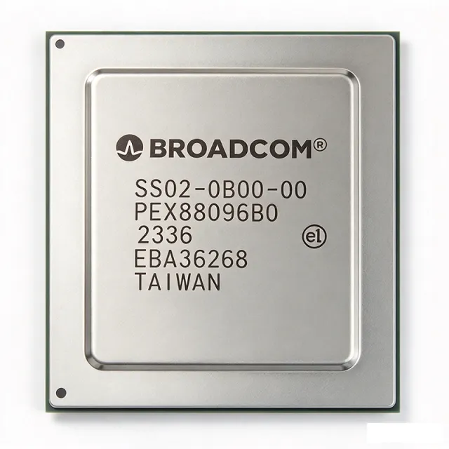
PEX88096B0-DB - 96-Lane PCIe 4.0 Switch | Broadcom | Storage
The Broadcom PEX88096B0-DB is a 96-lane PCI Express 4.0 managed switch from the PEX88000 series, delivered in a 1550-ball BGA package (37.5 x 42.5 mm) optimized for high-density storage and fabric applications. It provides 48 downstream ports and supports up to 98 solid-state drives through fan-out switching, while operating at the full PCIe 4.0 data rate of 16 GT/s per lane. A PCI Express (PCIe) switch is a high-speed serial fabric device that expands a single root-complex link into many endpoint links, enabling fan-out topologies in servers, storage arrays, and accelerator platforms. PCIe 4.0 is the fourth generation of the PCI Express standard, doubling the per-lane bandwidth of PCIe 3.0 to 16 GT/s. As a managed switch, the PEX88096 supports advanced features such as hot-plug, surprise-down recovery, dynamic port bifurcation, and Spread Spectrum Clocking (SSC) isolation, which are essential for enterprise storage and NVMe deployments. Key features include 96 total PCIe 4.0 lanes with 48 configurable downstream ports, integrated DMA and I/O virtualization support, hot-plug capability on every port, advanced error reporting (AER), and Broadcom's proprietary chip-link diagnostics. The device supports bifurcation configurations such as x4, x8, x16 per port and provides per-port signal-integrity tuning for reliable operation across long backplane traces. The 1550-ball BGA exposes a wide SERDES and sideband I/O complement suitable for adapter cards, backplanes, and custom ASIC/FPGA co-designs. Architecturally, the PEX88096B0 uses a non-blocking cut-through switching fabric with per-port credit-based flow control, multi-queue VC support, and a 32-bit MCU management interface. It is firmware-compatible with the broader PEX88000 family (including the PEX88064, PEX88080, and PEX88128), allowing OEMs to scale port count and lane count on a single software platform. Typical applications include NVMe SSD JBOD enclosures with 96+ drives, composable disaggregated storage fabrics, GPU/CPU accelerator pooling backplanes, hyperscale data-center storage tiers, and PCIe fan-out adapter cards. Both active and low-power standby states are exposed, making the device usable in dense thermal envelopes where chassis airflow is constrained. When designing with the PEX88096B0-DB, allocate at least six PCB layers with impedance-controlled 85 ohm differential SERDES routing, a dedicated reference clock distribution network with SSC support, and provide thermal management through the central heat-spreader pad. The on-chip microcontroller requires an external SPI flash for firmware boot.
PEX90144 - 144-Lane PCIe Gen6 Switch | Broadcom | AI
The Broadcom PEX90144 is a 144-lane PCI Express 6.0 packet switch built on a 5nm process, part of the Broadcom ExpressFabric PCIe switching family. It supports port widths of 2, 4, 8, or 16 lanes and delivers up to 256GB/s of bidirectional raw bandwidth per x16 port, with up to 9.2Tb/s of raw bandwidth achievable through the device in its largest configuration. A PCIe switch is a fabric device that expands a single root-complex PCI Express link into multiple downstream endpoints, aggregating GPU, NIC, storage controller, and accelerator traffic. In the system hierarchy, it sits between the host CPU root port and the endpoint tier, and is a core building block of modern data center interconnect fabrics alongside CPU PCIe controllers and retimers. Key differentiating features include hardware multi-host support for sharing the switch fabric across several hosts, an in-house Broadcom SerDes PHY exceeding 36dB of performance margin at Gen6 PAM-less NRZ data rates, and an embedded PCIe protocol analyzer for in-system debug without external interposer hardware. Turnkey fabric management software simplifies bring-up and topology configuration for large racks. Architecturally, the 5nm CMOS process integrates the SerDes, packet-routing fabric, and management engines on a single die, keeping per-lane power low while sustaining Gen6 64GT/s signaling. The device scales above its siblings, sitting as the widest device in Broadcom's published PCIe Gen6 switch lineup, which also includes 104-lane and 88-lane configurations. Typical applications include AI rack-scale connectivity between host CPUs and GPU accelerators, high-density server PCIe expansion chassis, composable and disaggregated infrastructure, and NVMe storage fabrics. It was publicly demonstrated integrated into a Dell PowerEdge XE7745-style PCIe board at SC25. Design consideration: at this bandwidth scale, signal-integrity planning for Gen6 64GT/s channels, substrate stack-up, and thermal design for the large BGA package are critical; consult the Broadcom PEX90000 series product brief for validated topologies. This page synthesizes distributor availability, family cross-references, and practical design guidance not found in the manufacturer datasheet.

PGA309AIPWR - Programmable Sensor Conditioner | TI | 16-TSSOP
The PGA309AIPWR from Texas Instruments is a voltage output programmable analog signal conditioner designed specifically for resistive bridge sensors. It integrates a precision analog signal path with digital calibration capabilities, enabling correction of zero, span, zero drift, span drift, and sensor linearization errors. Housed in a 16-pin TSSOP (PW) package, this device operates over a temperature range of -40°C to +125°C, making it suitable for industrial and automotive environments. A programmable sensor conditioner is an integrated circuit that amplifies and calibrates the small differential output of a bridge sensor, such as a strain gauge or pressure sensor, converting it into a linear, temperature-compensated voltage output. It sits between the sensor and the ADC or microcontroller, forming a complete sensor signal chain. This category falls under sensor interface ICs within the broader analog signal processing domain. Key features include a programmable gain amplifier (PGA) with adjustable gain, a digital-to-analog converter (DAC) for offset and span calibration, and an internal temperature sensor for drift compensation. The device supports a supply voltage up to 5.5V and provides a ratiometric or absolute voltage output. Its digital interface allows in-system calibration via a two-wire serial interface, simplifying production trimming. The PGA309 employs a chopper-stabilized amplifier architecture to achieve low offset and drift, ensuring high accuracy over temperature. The integrated calibration engine uses look-up tables to linearize the sensor response, reducing the need for external components. This architecture provides a complete, factory-calibrated solution that minimizes assembly cost and improves yield. Typical applications include industrial pressure transmitters, automotive manifold absolute pressure (MAP) sensors, and precision weigh scales. The device's wide temperature range and programmable features make it ideal for harsh environments where sensor accuracy is critical. When designing with the PGA309AIPWR, ensure proper decoupling of the supply pins and careful layout of the analog input traces to minimize noise. The calibration coefficients should be stored in an external EEPROM, as the device does not have non-volatile memory on-chip.
PI2DBS212ZHEX - 2-Channel Broadband Switch | Diodes
The Diodes Incorporated PI2DBS212ZHEX is a 2-channel differential broadband switch IC with a stated 1.2 V to 1.8 V single-supply range and a 28-pin TQFN package measuring 3.5 mm by 5.5 mm. It is categorized as a special-purpose analog switch and is intended for telecommunications signal routing. The verified distributor results also identify it as a dual 1:2 analog multiplexer, indicating that each channel can route a signal between multiple paths. An analog switch is a semiconductor-controlled routing element that connects or isolates circuit nodes with relatively low impedance in the selected state. In the broader hierarchy, this PI2DBS212ZHEX is a special-purpose analog switch, then an interface IC, then a semiconductor. Broadband switches are used where a signal must reach different downstream circuits with controlled insertion loss, isolation, and switching behavior. Their performance depends on supply voltage, signal amplitude, frequency, control logic, layout parasitics, and the impedance of the connected network. The PI2DBS212ZHEX is specified for single-supply operation from 1.2 V to 1.8 V. Two channels and differential broadband routing are its principal verified functional characteristics. The 28-TQFN package supports compact surface-mount layouts, while the exposed pad, where applicable, provides a thermal connection to the PCB. The available distributor snippets do not provide verified insertion loss, bandwidth, on-resistance, off-isolation, leakage, switching time, control thresholds, or absolute maximum ratings, so those values remain unavailable in this data set. Telecommunications equipment is the clearest fit because the manufacturer and DigiKey classify the device as a telecommunications switch. It may also be evaluated for broadband test paths, routing networks, and communication modules when its complete electrical limits satisfy the system requirements. The low 1.8 V upper supply limit is important: downstream circuitry must remain compatible with this range, and signal amplitudes must not exceed verified device limits that are not present in the supplied records. PCB implementation should follow the manufacturer pinout and land pattern once the official datasheet is obtained. Place power and ground connections directly to their assigned pins, keep high-frequency switched traces short, and minimize copper around sensitive routing nodes. Because exact pin names, control timing, and electrical characteristics are unavailable, a board should not be released for production until those details are verified against the official PI2DBS212 datasheet. This product record consolidates verified distributor identification, sourcing information, and design caveats while clearly separating known facts from missing technical data. It is intended to support early component selection, quotation requests, and engineering follow-up rather than replace the manufacturer datasheet or a completed signal-integrity evaluation.
PI2USB4122ZHEX - USB 3.2 Gen 1 4:1 Mux/DeMux Switch | Diodes Inc
The Diodes Incorporated PI2USB4122ZHEX is a high-performance USB 3.2 Gen 1 (formerly USB 3.0) 4:1 mux/demux switch IC housed in a 42-TQFN (9x3.5 mm) package with an exposed thermal pad. The device supports four differential channels that can be routed between one USB Type-C/USB 3.0 port and four possible source/sink endpoints, enabling switching of SuperSpeed USB (5 Gbps) signals with minimal insertion loss and return loss across the full USB 3.2 Gen 1 frequency spectrum. A USB switch (also called a USB mux/demux or USB crossbar switch) is a high-speed analog multiplexer designed to route USB 2.0 and SuperSpeed USB signals between multiple physical connectors or controllers while preserving signal integrity. As a category, USB switches sit within the broader hierarchy of analog switches and multiplexers -> signal switches -> interface ICs -> semiconductors. They are essential building blocks in any system that must share limited USB ports among multiple functions (charging, data, audio, debug), and they sit electrically downstream of the USB PHY and upstream of the physical connector. PI2USB4122 is the second-generation Diodes Inc. offering in this category and operates from a single 1.8 V supply rail, simplifying integration into modern low-voltage SoCs. Key differentiating features include 5 Gbps SuperSpeed USB channel support, low 5 ohm typical on-resistance per channel, -3 dB bandwidth exceeding 2.5 GHz to preserve USB 3.2 Gen 1 eye margins, 1.8 V single-supply operation, and integrated sideband/USB 2.0 pass-through routing. The exposed thermal pad on the TQFN package keeps the die-to-ambient thermal resistance low enough for hot-plug events without derating. The PI2USB4122 uses a wide-bandwidth CMOS pass-gate architecture with adaptive biasing to maintain flat frequency response up to 2.5 GHz. Internal ESD protection exceeds 2 kV HBM on the high-speed data lines, reducing external TVS diode count. The control logic accepts standard GPIO inputs for channel selection, allowing direct connection to a USB Type-C port controller without an external I/O expander. Typical applications include USB Type-C port multiplexers in laptops, tablets and docking stations, smartphone fast-charge/data switching paths, USB 3.0 hubs with multiple upstream ports, and Thunderbolt/USB4 sideband routing. The exposed-pad TQFN package makes it suitable for both handheld and dock designs where PCB real estate is constrained. When designing with this part, note the NRND (Not Recommended for New Design) status - the family remains in production for existing platforms but new designs should evaluate the PI3USB4122 or PI3USB31432 successors. Decoupling must include a 0.1 uF X7R cap on VCC placed within 2 mm of the exposed pad, and the high-speed differential pairs require 85 ohm differential impedance with matched trace lengths within the data-sheet tolerance window. This page synthesizes distributor pricing across DigiKey, Mouser, Arrow and LCSC, drop-in alternative candidates from the same Diodes Inc. family, and practical design notes drawn from the manufacturer datasheet - information not aggregated on any single distributor site.

PI3DBS16213XEAEX - PCIe Gen 4 MUX 12GHz Switch | Diodes Inc
The Diodes Incorporated PI3DBS16213XEAEX is a 2-channel, 3:1 PCIe Gen 4 multiplexer/switch IC that routes high-speed differential signals between a single common port and three separate downstream paths, delivering up to 12 GHz of -3 dB bandwidth for next-generation server and add-in-card applications. Housed in a 24-pin X1QFN (2x4 mm) exposed-pad package, the device operates from a 3.3 V supply and is rated for the industrial -40 °C to +85 °C temperature range with bidirectional analog switching on each channel. Background Knowledge: A PCIe multiplexer (MUX) is a type of high-speed analog switch that belongs to the broader family of analog switches and multiplexers used in digital interface ICs. PCIe switches sit within the signal-integrity layer between a host CPU/chipset and peripheral endpoints, allowing designers to share a single PCIe lane across multiple downstream devices (such as SSDs, NICs, or riser connectors). They are commonly deployed in storage backplanes, GPU workstations, and server riser cards where lane routing flexibility is required without expanding the host's native PCIe fan-out. Key features of the PI3DBS16213 include 12 GHz bandwidth enabling PCIe Gen 4 (16 GT/s) signaling, two differential channels for 4-lane packet switching capability, low insertion loss for signal-integrity compliance, and bidirectional flow-through pin assignment that simplifies PCB routing on inner stripline layers. The X1QFN-24 (2x4 mm) package exposes a thermal pad that ties to the system ground plane for EMI shielding and thermal dissipation. Architecturally, the device uses a passive FET-based switching matrix with minimal parasitic capacitance, optimizing return-loss and crosstalk figures required for PCIe Gen 4 link-training sequences. Internal bias generation on each channel reduces the BOM by eliminating external DC blocking caps on many reference designs. Typical applications include PCIe Gen 4 server backplanes, NVMe SSD port multipliers on storage enclosures, GPU workstation riser cards, and any design that needs to switch PCIe lanes between two downstream partners without unplugging cables. The 3.3 V single-rail operation is compatible with mainstream server auxiliary rails. Design consideration: maintain a continuous reference (ground) plane under the X1QFN exposed pad to achieve the datasheet's signal-integrity targets; non-continuous flex would degrade return loss at the Nyquist frequency of PCIe Gen 4 (8 GHz fundamental). Source impedance should target 85 Ω differential with skew matched to within 5 ps per channel. This page synthesizes distributor pricing, drop-in-compatible alternatives, application guidance, and engineering design notes not consolidated in the manufacturer brief, giving procurement and design engineers a single decision-ready reference.

PI3DPX1202A1ZB - DP 1.2 Redriver, 5.4Gbps, 48-TQFN | Diodes Inc
The Diodes Incorporated PI3DPX1202A1ZB is a low-power DisplayPort 1.2 redriver with integrated DDC/AUX channel switch, supplied in a 48-pin TQFN (7x7 mm) package. It supports all three DisplayPort 1.2 data rates - 1.62 Gbps (RBR), 2.7 Gbps (HBR) and 5.4 Gbps (HBR2) - and dual-mode DisplayPort (DP++) with TMDS clock frequencies up to 340 MHz, enabling HDMI interoperability through a passive adapter. The device presents a 1-channel high-speed signal path with internal 50 ohm input pull-downs, configurable output level and pre-emphasis, and an Aux Listener that supports link training. What is a DisplayPort redriver? A redriver (also called a signal repeater or retimer-less repeater) is a linear equalizer placed in series with a high-speed serial link. Unlike a retimer it does not add a clock-data-recovery block; instead it compensates for channel loss with adjustable input equalization and output de-emphasis, then re-drives the signal to restore eye-diagram margin. Redrivers sit between a source (GPU, SoC) and a sink (monitor, dongle) and belong to the signal-conditioning family of interface ICs alongside retimers, crosspoint switches and redrivers for USB, PCIe and HDMI. Key features include an ultra-low-power design (136 mA typical at 400 mVpp swing, 0 dB setting), pin-to-pin compatibility with the prior-generation PI3EQXDP1201, dual-mode (DP++/TMDS) input and output, integrated DDC/AUX channel switch, and selectable output level and pre-emphasis through external configuration. The 48-TQFN package combines an exposed thermal pad with a compact 7x7 mm body to fit space-constrained docking stations and embedded DisplayPort designs. The PI3DPX1202A1ZB uses Pericom's (now Diodes) proven linear-redriver architecture, with adaptive or fixed equalization that recovers the high-frequency content attenuated by PCB traces, cable assemblies, and connector transitions. This allows system designers to extend usable cable length, route signals through denser board layouts, or pass strict DisplayPort 1.2 compliance eye-mask tests at the connector. Typical applications include notebook docking stations, DisplayPort 1.2 graphics cards, motherboards with embedded DP outputs, DP-to-HDMI adapters (DP++/TMDS), 4K UltraHD monitors, and Thunderbolt accessory boards. The 5.4 Gbps HBR2 rate supports 4K@60 Hz (3840x2160) color-depth-rich video streams. When designing with this part, place the device as close as practical to the source connector to maximize the recovered signal integrity budget on the far end. Use the AC-coupling capacitors specified in the datasheet, follow the recommended reference-resistor values for the desired output swing, and respect the thermal-pad soldering guidelines for the 48-TQFN package. This page synthesizes distributor stock, same-family Diodes alternatives, and PCB-layout guidance beyond the manufacturer datasheet, with information gain not duplicated on DigiKey or Mouser product pages.

PI3DPX1202A1ZBE - 5.4Gbps DisplayPort 1.2 Redriver | Diodes Inc
The Diodes Incorporated PI3DPX1202A1ZBE is a low-power DisplayPort 1.2 redriver with integrated DDC/AUX channel switch, supplied in a 48-pin TQFN (V-QFN7070-48, 7x7 mm) package with exposed thermal pad. The device supports one channel at up to 5.4 Gbps data rate per lane, making it suitable for DisplayPort 1.2 (HBR2) source-side and sink-side signal conditioning. Per the Diodes datasheet, the PI3DPX1202A1 offers signal buffering/redriver functionality with integrated DDC/AUX multiplexer switching between source and sink. A signal buffer/redriver is a linear or adaptive repeater placed in series with a high-speed serial channel to compensate for channel loss caused by PCB traces, connectors, cables, or inter-symbol interference. It restores signal amplitude and rise/fall times without re-timing the data (a redriver is protocol-transparent), which is critical for DisplayPort, HDMI, USB 3.0, and PCIe Gen2/Gen3 links where budgets may be exceeded by the physical medium. Within the broader component taxonomy, a redriver sits below retimers (which recover clock/data) and above simple repeaters, and it belongs to the Interface ICs > Signal Buffers, Repeaters family of mixed-signal analog conditioning products. Key features include 5.4 Gbps per-lane support (DisplayPort HBR2), adaptive equalization to compensate for frequency-dependent channel loss, transmit de-emphasis to reduce inter-symbol interference at the source, integrated DDC/AUX switch for source/sink routing, low standby current, and 3.3 V single-supply operation. The TQFN-48 (7x7 mm) package with exposed pad provides a low thermal resistance path for surface-mount designs. Internally, the redriver combines a CTLE-style adaptive equalizer at each input with a fixed or selectable de-emphasis driver at each output, plus auxiliary logic for DDC/AUX channel switching. The equalizer extends the usable channel length at HBR2 (5.4 Gbps) where 28 AWG cable losses exceed 10 dB at the Nyquist frequency. The DDC/AUX switch supports bidirectional auxiliary and EDID transactions without an external mux. Typical applications include notebook docking stations, monitor input panels, DisplayPort dongles and adapters, embedded display boards, video capture cards, and any compact DisplayPort source/sink where PCB trace or cable length exceeds the native 8-10 dB loss budget at HBR2 rates. When designing with this part, place it within 4 inches of the DisplayPort connector; provide a solid 3.3 V decoupling network (10 uF bulk + 0.1 uF/0.01 uF high-frequency) at VCC; and route the high-speed TX/RX pairs with 100 ohm differential impedance and length matching within 5 mils per pair. This page synthesizes distributor pricing, drop-in same-package alternatives from the Diodes DisplayPort redriver family, DDC/AUX mux companion parts, and practical PCB layout notes not aggregated in the manufacturer datasheet.
PI3USB102GZLEX - USB 2.0 2:1 Switch with 5V Protection | Diodes Inc
The Diodes Incorporated PI3USB102GZLEX is a high-performance USB 2.0 high-speed switch configured as a single differential channel 2:1 multiplexer/demultiplexer, packaged in a 10-pin TQFN (1.3x1.6 mm) with an exposed thermal pad. It supports USB 2.0 high-speed (480 Mbps) signaling, offers low on-resistance (5 ohm max), a 1 GHz -3 dB bandwidth, and integrated 5V over-voltage protection on Y+/Y- pins per USB 2.0 specification, allowing all I/O pins to withstand Vbus shorts (5V +/- 10%) whether the chip is powered on or off. A USB switch is a specialized analog multiplexer designed to route USB 2.0 differential pairs between two physical ports or between a single port and a downstream controller. It belongs to the broader family of analog switches and multiplexers, which sit under interface ICs in the semiconductor taxonomy. These parts are critical in systems where one USB physical-layer transceiver must service multiple connectors, OTG roles, USB Type-C role swaps, dock/multi-connector designs, or test-mode path selection. By isolating one data path while activating another, the switch lets one SoC PHY serve two USB connectors without contention. Key differentiating features include very low bit-to-bit skew, high channel-to-channel noise isolation, flow-through pinout for simplified PCB routing, and an improved Ioff voltage range that reduces leakage when VCC is removed. Bidirectional operation means it supports both host-side and device-side roles equally well, and it operates across the -40C to +85C industrial temperature range. The 10-TQFN (1.3x1.6) footprint measures only 2.08 mm^2, enabling it to fit comfortably inside USB connector shields, Type-C mid-mount boards, and dongle-class products. Typical applications for the PI3USB102GZLEX span consumer tablets, notebooks, dock stations, USB Type-C adapters, OTG phones, and any system that needs to share one USB 2.0 PHY between two physical ports. Inside a tablet, for example, it sits between the SoC's USB pins and the system micro-USB or Type-C connector, providing 5V Vbus short protection for the SoC's USB lines. The part can also multiplex between an internal USB header and an externally accessible connector for service-mode diagnostics or docking. When designing with the PI3USB102GZLEX, place the device adjacent to the USB connector so the 5V Vbus short protection works as close to the system boundary as possible. Use a 100 nF decoupling capacitor close to VCC, and follow the USB 2.0 differential pair impedance target of 90 ohm differential. When the chip is powered down, signal leakage through the switch is dominated by Ioff, so confirm this does not exceed downstream PHY leakage budgets. This page synthesizes distributor pricing, drop-in same-package alternatives, and practical PCB design considerations - information that goes beyond what is found in the manufacturer datasheet alone.

PI3VST01UE - VGA HPD Signal Generator | MSOP-8 | Diodes
The Diodes Incorporated (formerly Pericom) PI3VST01UE is a single-channel VGA Hot Plug Detect (HPD) signal generator IC housed in an 8-pin MSOP (Mini Small Outline Package). The device generates a buffered HPD logic signal used in legacy VGA connectors, supporting DisplayPort-to-VGA adapters, docking stations, and monitor-side hot-plug detection circuits where a clean, low-jitter logic-level assertion is required. Key features include a wide 3.0 V to 5.5 V single-rail supply range, CMOS/TTL-compatible HPD output, low quiescent current draw suitable for always-on bias rails, and an integrated pull-up on the HPD output pin per the VESA-recommended 1 kohm impedance. The MSOP-8 surface-mount package is footprint-compatible with standard industry pinouts and supports automated PCB assembly. The PI3VST01UE is a specialized analog mixed-signal interface IC belonging to the analog switch / special-purpose switch family (also classifiable as a video interface switch). Within the broader component taxonomy it sits under interface ICs, video ICs sub-category, semiconductor -> integrated circuit -> analog mixed-signal IC -> HPD signal generator. Its function is to provide electrical buffering and level translation of the HPD logic signal that source devices use to detect cable presence on VGA/DisplayPort output chains. Typical applications include DisplayPort-to-VGA adapters, video docking stations, monitor-side cable-presence detection on VGA inputs, KVM switches that must expose HPD to a graphics source, and legacy graphics cards that lack a native HPD output stage. It is also used in industrial video distribution equipment where hot-plug events must be regenerated cleanly to avoid host GPU re-enumeration glitches. When designing with this device, observe standard ESD precautions on the VGA DDC/HPD lines and decouple VCC with at least a 0.1 uF ceramic capacitor placed within 5 mm of the supply pin. The exposed pad on the MSOP-8 should be soldered to the PCB ground plane for thermal performance and pin-1 reference accuracy. This page synthesizes distributor pricing (DigiKey, Mouser, Octopart), package-level cross-references, drop-in alternatives, and PCB-level design notes into a single reference that is not duplicated on the manufacturer datasheet.