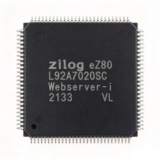
EFM32ZG222F4-B-QFP48
EFM32ZG222F4-B-QFP48 - 24MHz ARM Cortex-M0+ MCU | Silicon Labs
Silicon Labs EFM32ZG222F4-B-QFP48 is a 32-bit ARM Cortex-M0+ microcontroller rated up to 24 MHz, with 4 KB of flash memory, 2 KB of RAM, and 37 digital I/O pins in a 48-pin TQFP package. The device operates from 1.98 V to 3.8 V and is designed for energy-sensitive embedded systems that require low-power operation, fast wake-up behavior, and integrated peripherals.
A microcontroller is a programmable system-on-chip that combines a processor core, memory, digital I/O, timers, analog interfaces, and communication peripherals. The EFM32 Zero Gecko family belongs to the 32-bit MCU and embedded-controller hierarchy, combining an Arm Cortex-M0+ core with energy-saving modes suitable for battery-powered, industrial, and connected equipment.
Key features include a maximum 24 MHz processor clock, 4 KB flash, 2 KB RAM, 37 digital I/O pins, and two 16-bit timers. According to the Silicon Labs EFM32ZG data sheet, the family consumes as little as 0.5 µA in Stop mode and 114 µA/MHz in Run mode. These figures make the device appropriate for meter, sensor-node, and portable applications where average energy use matters more than peak processing throughput.
The EFM32 architecture emphasizes autonomous peripherals, fast transitions between low-energy states, and extensive analog and digital integration. Its Cortex-M0+ core supports efficient event-driven control, while its timers and communication peripherals can reduce the need for continuous central-processor intervention. This architecture is especially useful in systems that must periodically acquire data, process it locally, and sleep for most of the operating cycle.
Typical applications include smart energy meters, gas and water meters, industrial sensor nodes, compact environmental monitors, and battery-powered accessories. The 37 digital I/O pins provide interface flexibility for sensors, switches, indicators, and external converters, while the 48-pin TQFP package supports conventional surface-mount assembly and prototype-board routing.
Designers should preserve the device's decoupling and exposed-ground requirements, follow the recommended pin multiplexing in the manufacturer pin-description table, and validate firmware against the selected clock, flash, and peripheral configuration. If software must operate with a larger firmware image or RAM working set, choose a member with sufficient memory rather than changing code without a complete peripheral and memory-map review.
This product record combines manufacturer specifications, package details, verified sourcing information, and same-family drop-in alternatives. It also identifies memory-capacity trade-offs that matter when evaluating replacements, while keeping package and pin compatibility as the central PCB-level constraints.
RFQ
Contact