Power Management
Subcategories
Products (2,800+)

LM2675M-5.0/NOPB - 1A, 5V Fixed SIMPLE SWITCHER Buck Regulator | Texas Instruments
The Texas Instruments LM2675M-5.0/NOPB is a SIMPLE SWITCHER high-efficiency 1A step-down (buck) voltage regulator with a fixed 5V output, accepting a 6.5V to 40V input range and housed in an 8-pin SOIC (D) package with 0.154 inch (3.90 mm) body width. Designed as a monolithic LMDMOS-based regulator, it requires a minimum number of external components to deliver a complete DC-DC conversion solution. Key specifications include a 1A continuous output current rating, a 260 kHz internal oscillator that enables small magnetics, and ±1.5% output voltage tolerance over the specified input and load range. The fixed 5V version is internally trimmed, while the ADJ variant sets output via an external resistor divider. The LM2675 family falls within the broader category of switching regulators (buck converter -> step-down regulator -> DC-DC converter -> power management IC), designed to replace older three-terminal linear regulators with significantly higher efficiency. The LM2675M-5.0/NOPB features built-in thermal shutdown, cycle-by-cycle current limiting, and an on/off enable input for power sequencing. The internal MOSFET switch and CMOS gate driver are integrated on the same die, eliminating the need for an external power switch. Its wide 6.5V to 40V input range supports 12V and 24V industrial bus rails directly, while the fixed 5V output is well-suited to powering logic, microcontrollers, and 5V subsystems. Typical applications include point-of-load regulation in industrial equipment, distributed 5V rails in automotive subsystems, distributed power architectures fed from 12V or 24V buses, and battery-powered systems where efficiency matters. The low external component count also simplifies manufacturing and reduces BOM cost. When designing with the LM2675, follow the datasheet inductor and capacitor selection guides closely - choosing a low-ESR input capacitor and a Schottky catch diode rated for the switching current is essential for stable operation. The PCB layout should keep the catch diode loop and the feedback trace short to avoid injecting switching noise into the output. This page synthesizes distributor pricing, drop-in alternatives, and practical design notes not found in the manufacturer datasheet, giving engineers a single reference for sourcing, selection, and PCB-level integration of the LM2675M-5.0/NOPB.

LM2676S-ADJ/NOPB - 3A Step-Down Switching Regulator | Texas Instruments
The Texas Instruments LM2676S-ADJ/NOPB is a SIMPLE SWITCHER high-efficiency 3A step-down (buck) DC-DC regulator housed in a 7-pin TO-263 (D2PAK, KTW) surface-mount package with exposed thermal tab. It delivers an adjustable positive output from 1.2V to 37V from an 8V to 40V input rail, with up to 3A continuous load current and typical line/load regulation of better than 1%. A buck (step-down) switching regulator is a power-management IC that converts a higher DC input voltage to a lower DC output voltage by alternately storing energy in an inductor and releasing it to the load through a MOSFET switch. Within the system hierarchy, the LM2676 belongs to the SIMPLE SWITCHER family of non-isolated buck regulators, which sit within DC-DC switching regulators, which themselves are a sub-category of power-management ICs (PMICs). Compared with linear regulators (LDOs), buck converters like the LM2676 trade higher efficiency (typically 75-90%) for added complexity (inductor, catch diode, input/output capacitors) and produce switching ripple that must be filtered. Key features include a fixed 260 kHz switching frequency that allows use of small magnetic components, an internal DMOS power switch rated for 45V, a low quiescent current of 4.2 mA in standby, thermal shutdown, current limit, and an on/off enable control. The TO-263-7K-T package has a low thermal resistance (junction-to-case) of approximately 2 C/W, enabling full-power operation with a small copper heatsink area or none at all in low-duty applications. The device uses TI's classic buck control topology with voltage-mode control and internal compensation, simplifying external component selection. The feedback pin uses an external resistor network, while a soft-start capacitor controls soft-start discharge to limit inrush current during power-up. The high-side DMOS switch achieves low Rds(on) for high efficiency at 3A loads, making the LM2676S-ADJ/NOPB well-suited for medium-power point-of-load conversion. Typical applications include industrial 24V bus regulation, automotive accessory power (post-transient protection), battery-powered equipment, distributed 5V/12V/15V/24V rails in instrumentation, point-of-load regulation downstream of a rectifier, and high-current single-rail or front-end conversion. The wide input-to-output ratio and 3A capability cover most moderate-power distributed-power requirements. Design considerations: the catch diode with current limiting must be a Schottky type rated for the input voltage (e.g., 40V+ SS34), the inductor is typically 22-33 µH for most VIN/VOUT combinations, and the feedback divider must use 1% resistors. Because the LM2676 is not pin-compatible with newer TI WEBENCH-optimized regulators like the LMR33630, redesigns may be required for footprint migration, though the simple external BOM is widely documented and supported.

LM2755TMX - Charge Pump LED Driver, I2C, 3-LED, 18-DSBGA | TI
The Texas Instruments LM2755TMX is a charge-pump-based constant-current LED driver with I2C-compatible digital interface, capable of driving up to 3 LEDs with a total output current of 90 mA from a single-cell Li-ion source. Housed in a compact 18-ball DSBGA (Micro SMD) package, it integrates a fractional switched-capacitor (1x/2x) charge pump, three matched current sinks, and full I2C programming of brightness, ramp, and timing parameters. The device operates from a 2.7 V to 5.5 V input and supports diode waveforms with programmable rise time, fall time, high level, low level, delay, high time, and low time. A charge pump is a DC-DC switching converter that uses capacitors instead of inductors to step up or invert a voltage, multiplying the input by a fixed ratio (1x, 1.5x, or 2x). In a portable LED backlight system, the LED driver sits in the power management signal chain between the battery/power-management IC (PMIC) and the LED string. As a "linear regulator > voltage regulator > power management IC > semiconductor" hierarchy member, the LM2755 combines energy conversion with deterministic current regulation, making it ideal for thin display modules that cannot accommodate an inductor. Key features of the LM2755TMX include 90 mA total LED current across 3 outputs (30 mA per channel), 32-level I2C brightness control, programmable fade-in/fade-out ramps, and 1.2 MHz typical charge-pump switching frequency that allows the use of small 1 uF ceramic flying capacitors. An integrated soft-start limits inrush current, and over-temperature shutdown protects the device during fault conditions. The I2C interface supports 400 kHz Fast Mode and provides access to status registers for fault and identification. The LM2755 uses a dual-mode charge pump architecture that automatically switches between 1x pass-through and 2x boost to maximize efficiency across the Li-ion discharge curve, achieving roughly 93% peak efficiency at 3.7 V VIN driving white LEDs at 20 mA. Three independent current sinks with 1% current matching ensure uniform display brightness across RGB indicator or keypad applications. Typical applications include mobile-phone keypad backlighting, RGB status indicators, camera flash (low-current indicator LEDs), portable medical-device displays, and wearable activity-tracker indicator LEDs. The wide 2.7 V to 5.5 V input range also supports USB-powered and 1-cell Li-ion designs directly without a pre-regulator. When designing with this device, observe the 18-ball DSBGA layout guidelines strictly - the device requires a four-layer PCB with a continuous ground plane and vias under the thermal pad to dissipate up to 0.5 W. The I2C address is fixed (0xC8 7-bit), so multiple LM2755 instances on the same bus are not supported; for multi-channel designs, select the LM2756/LM2757 family instead. This page synthesizes distributor pricing, verified drop-in alternatives, and practical design notes not found in the manufacturer datasheet.

LM2841XMK-ADJL/NOPB - 300mA 42V Step-Down DC/DC | Texas Instruments
The Texas Instruments LM2841XMK-ADJL/NOPB is a 300 mA, 42 V input-capable SIMPLE SWITCHER® step-down (buck) DC-DC regulator housed in a 6-pin Thin SOT-23 (TSOT-23-6, TI DDC package). It accepts 4.5 V to 42 V inputs and produces an adjustable output from 0.765 V up to 39.48 V, making it well suited to industrial and automotive load-dump-tolerant point-of-load regulation. According to the TI LM2841 product page, the family comprises the LM2840 (100 mA), LM2841 (300 mA), and LM2842 (600 mA), all built around a 0.765 V nominal feedback reference. A buck (step-down) DC-DC converter is a switch-mode power supply topology that efficiently converts a higher DC input voltage into a lower DC output voltage by rapidly chopping the input with an inductor-capacitor filter network, achieving efficiencies that linear regulators cannot match at large input-to-output differentials. Within the broader power management IC hierarchy, the LM2841XMK sits under DC-DC converters -> voltage regulators -> power management ICs -> semiconductors. The TSOT-23-6 (DDC) footprint places it firmly in the surface-mount QFN/SOT family, and its wide VIN range makes it a common choice for 12 V/24 V industrial bus and battery-powered applications. Key features of the LM2841XMK include a wide 4.5 V to 42 V continuous input range, an integrated MOSFET switch that keeps the BOM small, 300 mA continuous output current, a low 0.765 V feedback reference, internal compensation that removes the need for an external compensation network, and a shutdown (SHDN) pin that can implement soft-start with an external RC. Its 1.25 MHz nominal switching frequency allows small ceramic input/output capacitors and a tiny inductor, shrinking the total solution footprint to a few square millimeters on the PCB. Typical applications for the LM2841XMK include 12 V/24 V industrial sensor rails, battery chargers, LED drivers, distributed supply rails in point-of-load systems, and any application that needs to step a wide-range bus down to a logic-level rail. It is frequently selected over linear regulators when the input-to-output differential exceeds ~2 V because of its high efficiency. The thin SOT-23 package has a theta-2-JA around 90 C/W on a standard JEDEC test board, so careful copper-pour thermal management is required when dissipating more than ~0.5 W. When designing with the LM2841XMK, follow the manufacturer datasheet recommended inductor and capacitor values for your specific VOUT, and ensure the input capacitor handles the RMS ripple current at the 1.25 MHz switching frequency. Always check that the peak inductor current stays below the 0.5 A peak switch-current limit when the load transient peaks coincide with minimum VIN. This page synthesizes distributor pricing, drop-in alternatives, and practical design notes not found in the TI datasheet alone.
LM2841YMK-ADJL - 300mA 42V Buck Converter | Texas Instruments
The Texas Instruments LM2841YMK-ADJL is a 300 mA, 42 V input-capable PWM DC/DC buck (step-down) switching regulator with adjustable output voltage (0.765 V minimum reference), housed in a 6-pin thin SOT-23 (TSOT-23-6 / DDC) package. It integrates a 0.9 ohm typical low-RDS(ON) internal power switch, enabling typical efficiency of 85 percent from wide-input industrial and consumer rails. The switching frequency is 1500 kHz nominal, allowing the use of small external inductors and ceramic output capacitors. What is a buck converter? A buck converter (step-down DC/DC switching regulator) is a power management device that uses an internal MOSFET switch, an inductor, and a capacitor network to convert a higher DC input voltage to a lower regulated DC output voltage with high efficiency. Buck converters sit in the power management taxonomy as: buck converter -> DC/DC switching regulator -> voltage regulator -> power management IC. They are preferred for higher step-down ratios where linear regulators (LDOs) waste excessive power as heat. Key features include a 4.5 V to 42 V wide input range that tolerates automotive load-dump conditions and 24 V industrial buses, internal compensation that eliminates most external compensation components, and built-in cycle-by-cycle current limit, thermal shutdown, and soft-start on the same enabling reference family. The thin SOT-23-6 footprint occupies approximately 9 mm² of board space, suiting space-constrained point-of-load applications. Architecturally, the device uses a fixed-frequency peak-current-mode control topology. The internal high-side switch commutates the inductor at 1.5 MHz, and the feedback loop regulates the output against the 0.765 V internal reference using an external resistor divider. The peak-current-mode control provides inherent cycle-by-cycle current limiting and simplifies loop compensation. Operating junction temperature spans -40 C to +125 C, supporting automotive and industrial environments. Typical applications include point-of-load regulation for 24 V industrial buses, powering microcontrollers and sensors from unregulated 12 V or 18 V sources, portable and battery-powered systems, LED constant-current drivers, and automotive infotainment and body electronics. The wide input range also supports wall-transformer-fed consumer electronics, telecom point-of-load rails, and distributed supply architectures. When designing with this regulator, ensure the input capacitor and bootstrap capacitor are placed close to the IC pins and that the inductor is sized for 1500 kHz operation (typically 4.7 uH to 22 uH). Calculate power dissipation by (I_OUT × V_DIODE) for the rectifying path and (I_OUT × VIN × (1 - VOUT/VIN)) for the high-side switch, then verify thermal margin against the 31.6 C/W theta_JA in TSOT-23. This page synthesizes distributor stock and pricing, drop-in alternatives across TI and competing brands, and practical PCB/thermal design notes not found in the bare datasheet.
LM2936BMX-3.3/NOPB - 50mA, 40V Ultra-Low IQ LDO | Texas Instruments
The Texas Instruments LM2936BMX-3.3/NOPB is a 50 mA, fixed 3.3 V output, ultra-low quiescent current low-dropout (LDO) linear regulator with reverse-voltage protection, packaged in an 8-pin SOIC (D). It is the tape-and-reel, Pb-free, RoHS-compliant variant of the LM2936-3.3 family and is qualified for automotive and battery-operated applications where standby current is critical. An LDO (Low-Dropout) linear regulator is a type of voltage regulator that maintains a stable output voltage even when the input voltage is only slightly above the output voltage. LDOs sit within the broader power management IC hierarchy as linear regulators (versus switching regulators), trading efficiency for simplicity, low noise, and very small quiescent current. The LM2936 family specifically targets always-on battery and automotive subsystems. Key features include a 5.5 V to 40 V (60 V transient-tolerant) input operating range, 3.3 V fixed output with ±3% accuracy over line, load, and temperature, 200 mV typical dropout at 50 mA, and ultra-low quiescent current of approximately 20 uA (typ) at light loads. The reverse-voltage protection block prevents damage from reversed battery or load-dump transients common in 12 V automotive rails, and internal current limit plus thermal shutdown provide additional robustness. The architecture uses a PNP pass element followed by a precision bandgap reference, allowing the regulator to operate with very low quiescent current while maintaining regulation down to small VIN-VOUT differentials. The -40C to +125C junction temperature range and automotive-grade qualification make it suitable for under-hood and body-control modules. Typical applications include automotive body electronics and ECU standby rails, battery-powered microcontroller sleep-mode supplies, keep-alive RAM retention in parking/telematics modules, HVAC sensor bias, and remote/keyless-entry receiver power. The 40 V rating also makes it well-suited to industrial 24 V bus systems. When designing with this device, keep input and output capacitors close to the pins and verify the dropout margin at minimum VIN. Reverse-polarity and load-dump events must still be mitigated externally for full automotive transient compliance. This page synthesizes distributor pricing, drop-in same-package alternatives, and practical design notes not consolidated on the manufacturer datasheet, enabling faster BOM decisions for 3.3 V always-on rails.

LM317AMDTX/NOPB - 1.5A Adjustable Linear Regulator, TO-252 | Texas Instruments
The Texas Instruments LM317AMDTX/NOPB is a 1.5-A, 40-V, high-accuracy adjustable three-terminal positive linear voltage regulator in a 3-pin TO-252 (DPAK) surface-mount package. It delivers adjustable output from 1.25 V to 37 V at up to 1.5 A with 1% output voltage accuracy and full overload protection including current limit, thermal shutdown, and safe-area compensation. The device is supplied on tape-and-reel (suffix TX) with the lead-free / no-PB (NOPB) finish. An adjustable linear regulator (often called a three-terminal regulator) maintains a stable output voltage set by an external resistor divider, while dissipating the difference between input and output voltage as heat. These regulators form the simplest building block in the power-management hierarchy: linear regulator -> voltage regulator -> power management IC -> semiconductor. They trade efficiency for low noise, simplicity, and low cost versus switching converters, and are ideal when a few watts of dissipation are acceptable and noise-sensitive analog or digital loads must share a clean rail. Key electrical characteristics include a 4.2 V to 40 V input range, 1.25 V to 37 V adjustable output, typical 1.5 A load current with peak capability exceeding 1.5 A, line regulation of 0.01%/V (typical), and load regulation of 0.1% (typical). Internal protection covers thermal-overload, short-circuit current foldback, and safe-operating-area compensation. The DPAK (TO-252) tab serves as the heatsink, allowing moderate dissipation directly into PCB copper without a discrete heatsink. Typical applications include local post-regulation after a switching converter, bench power supplies, battery chargers, LED current regulators, and industrial 24 V bus regulation. It is commonly used as a precision current source by setting R1 between VOUT and ADJ to program a constant 1.25 V across the sense resistor. When designing with the LM317AMDTX/NOPB, an input bypass capacitor is recommended if the regulator is more than 6 inches from the filter capacitor of the supply, and an output capacitor (tantalum or low-ESR aluminum) improves transient response. Calculate worst-case power dissipation as (VIN(max) - VOUT(min)) x IOUT(max) and ensure the copper area on the tab keeps junction temperature below 125 C. This page synthesizes distributor pricing, same-brand drop-in alternatives, cross-brand equivalents, and practical design notes not found in the manufacturer datasheet.

LM317DCYR - 1.5A Adjustable Positive Regulator | Texas Instruments
The Texas Instruments LM317DCYR is a three-terminal adjustable positive voltage regulator capable of supplying more than 1.5A over an output voltage range of 1.25V to 37V, housed in a compact SOT-223-4 surface-mount package. Only two external resistors set the output voltage, making it one of the most widely used linear regulators in electronics history. A linear regulator maintains a constant output voltage by dissipating excess power as heat. The LM317 is an adjustable linear regulator whose output is programmed by a resistor divider, with a fixed 1.25V reference between the output and adjustment pins. Linear regulators belong to the broader power management IC family, alongside switching regulators and LDOs, and are preferred in noise-sensitive circuits for their low output noise and fast transient response. Key features include typical line regulation of 0.01% and load regulation of 0.1%, plus internal short-circuit current limiting, thermal overload protection, and safe-area compensation. The device supports input voltages up to 40V, with a typical dropout voltage of about 2.5V at 1.5A load. The junction temperature range of 0C to 125C covers commercial and industrial requirements. Architecturally, the LM317 uses a bandgap reference and error amplifier. The 1.25V reference across the programming resistor makes the device double as a precise constant-current source, useful for LED driving and battery charging. The SOT-223-4 package offers good thermal performance with a reasonable PCB copper area, and the tab is connected to the output pin for direct heatsinking to a copper pour. Typical applications include adjustable bench power supplies, battery chargers, LED constant-current drivers, audio equipment, instrumentation, and industrial control systems where a stable adjustable rail is required. Design tip: maintain at least a 3V input-output differential for regulation, size copper pour for thermal dissipation, and bypass the adjustment pin with a capacitor to improve ripple rejection.

LM317LCPK - 100mA Adjustable Positive Regulator | Texas Instruments
The Texas Instruments LM317LCPK is a 3-terminal adjustable positive voltage regulator capable of supplying up to 100 mA over an output voltage range of 1.25V to 37V, housed in the compact SOT-89-3 (PK) package. It requires only two external resistors to set the output voltage, making it exceptionally easy to use in space-constrained designs. A linear voltage regulator is a type of voltage regulator that maintains a constant output voltage by dissipating excess power as heat. The LM317L belongs to the broader family of positive adjustable linear regulators, alongside fixed-output regulators like the LM78xx series and modern low-dropout (LDO) regulators. As a linear regulator, it offers low output noise and fast transient response, but is less efficient than a switching regulator when the input-to-output differential is large. Key features include the 100 mA output current, the wide 1.25V to 37V adjustable output, typical line regulation of 0.01%/V, and 30 uVrms output noise. Internal current limiting, safe-area compensation, and thermal overload protection are built in. The LM317LC series is characterized for a junction temperature range of 0C to +125C. Technically, the LM317L uses a bandgap reference and an error amplifier. The output voltage follows the classic formula VOUT = 1.25V * (1 + R2/R1) + IADJ * R2, with a 1.25V reference and 50 uA adjustment pin current. Typical quiescent (adjustment pin) current is low, and the SOT-89-3 tab provides improved thermal dissipation versus SOT-23 packages. Typical applications include on-board regulation for microcontrollers, analog sensor interfaces, low-power audio circuits, and battery-powered devices where a stable adjustable rail is required. Design tip: maintain at least 3V input-to-output headroom, keep input and output capacitors close to the device, and solder the tab to a copper pour for heat dissipation at higher VIN-VOUT deltas.
LM317LD13TR - 1.2-37V Adjustable LDO | STMicroelectronics
The STMicroelectronics LM317LD13TR is an adjustable positive linear voltage regulator with a 1.2 V to 37 V output range, low-current operation, and an SO-8 package. It is designed to regulate higher-voltage supplies down to a user-selected output using external resistors. The verified distributor listing identifies a 100 mA output-current configuration, while the datasheet result describes the device as a low-current adjustable regulator with a 1.2 V to 37 V range. Its positive output polarity, adjustable architecture, and internal thermal and short-circuit protection make it useful for low-power analog, instrumentation, control, and laboratory supply rails. The LM317LD13TR belongs to the LM317 family, whose defining feature is a simple three-terminal implementation: input, output, and adjustment. Unlike a switching regulator, the LM317 family provides low switching-related noise, but power dissipation depends on the difference between input and output voltage and load current. Applications include sensor excitation, reference rails, analog signal conditioning, small embedded supplies, and educational power-supply platforms. Because the SO-8 package is compact, PCB layout should provide adequate copper area and short, low-resistance paths for input and output connections. The adjustment pin requires a suitable compensation network to maintain loop stability, and the regulator should be checked for thermal rise at the maximum expected VIN, VOUT, and load. The LM317 family is also widely used where a simple, serviceable, and widely understood regulator topology is preferred over a more complex digital power solution.

LM317QDCYRQ1 - 500mA 40V Adjustable LDO | TI | Automotive
The Texas Instruments LM317QDCYRQ1 is an automotive-grade, positive adjustable linear voltage regulator delivering up to 500 mA of output current from a 40 V maximum input, packaged in a 4-pin SOT-223 (DCY) surface-mount package. As part of the LM317MQ family qualified for automotive applications, it provides a classic three-terminal adjustable regulator architecture with a 1.25 V reference voltage set by two external resistors. An adjustable linear regulator (LDO-style series pass regulator) is a type of voltage regulator that maintains a stable output voltage by controlling the voltage drop across an internal series pass transistor. Within the power management IC hierarchy, the LM317 family sits in the classic NPN-darlington floating regulator category, renowned for decades of use across industrial and automotive power rails. The 'Q1' suffix indicates AEC-Q100 qualification and automotive temperature support. Key features include a wide input voltage tolerance up to 40 V, 500 mA output current capability, internal thermal overload protection (thermal shutdown), and safe-operating-area current limiting. The floating architecture allows operation at high voltages, and the adjustable output enables a single design to cover multiple rail voltages simply by changing two resistors. Technically, the device regulates the 1.25 V bandgap reference between the output and adjustment (ADJ) pin. The load and line regulation benefit from the low reference current, and the ADJ pin current of approximately 50 uA must be accounted for in the output divider calculation for best accuracy. Standard 1% resistors typically achieve output accuracy within a few percent. Typical applications include automotive body electronics and infotainment auxiliary rails, industrial 12 V and 24 V bus post-regulation, and general-purpose adjustable bench or bias supplies where simplicity and robustness outweigh efficiency. Design consideration: the device is a linear regulator, so power dissipation equals (VIN - VOUT) x ILOAD. The SOT-223 tab should be soldered to a generous copper pour; verify junction temperature stays below the datasheet maximum at worst-case load and input voltage.
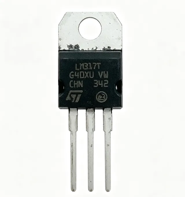
LM317T - 1.5A Adjustable 1.2-37V Regulator | STMicroelectronics
The STMicroelectronics LM317T is a three-terminal adjustable positive linear voltage regulator rated for 1.5A output current and an adjustable output range of 1.2V to 37V, supplied in a TO-220 package. It requires only two external resistors to establish the output voltage and provides internal current limiting, thermal overload protection, and safe-area compensation. An adjustable linear voltage regulator maintains a nearly constant output by operating a pass transistor in its linear region and correcting the output through feedback. The LM317T belongs to the linear regulator and voltage regulator branches of power-management ICs. Compared with switching regulators, it introduces little switching ripple and needs few external components, but its efficiency falls as input-to-output voltage difference and load current increase. Key electrical features include typical line regulation of 0.01% per volt and typical load regulation of 0.1%. The internal architecture regulates a nominal 1.25V reference between the output and adjustment pins. Internal current limiting limits fault current, thermal overload protection shuts down excessive temperature conditions, and safe-area compensation improves robustness when input and output conditions approach the pass transistor limits. The regulator uses a bandgap reference, error amplifier, and power pass transistor. Its output follows VOUT = 1.25V × (1 + R1/R2) plus the adjustment-pin current contribution, making resistor tolerance relevant to overall accuracy. The verified source data states an input-to-output differential range of 3V to 40V and a typical dropout voltage of 2V at a 1.5A load. Typical applications include adjustable laboratory supplies, battery chargers, constant-current sources, local regulation for audio and instrumentation, and general-purpose power rails. The TO-220 body is readily heatsinked, making the device practical when several watts must be removed, although allowable dissipation depends on junction temperature and thermal resistance. Designers should preserve at least the required input-to-output headroom, use a suitable heatsink, place input and output capacitors close to the device, and consider adjustment-pin bypassing for ripple rejection. Protection diodes may be needed when output capacitance creates discharge current through the regulator. This page also synthesizes verified source data, drop-in candidates, and practical engineering guidance beyond the basic datasheet description.

LM3404HVMAX/NOPB - 75V 1A Buck LED Driver SOIC-8 | Texas Instruments
The Texas Instruments LM3404HVMAX/NOPB is a 1.0 A constant-current step-down (buck) switching regulator designed to drive high-power LEDs from a wide 6 V to 75 V input supply, housed in an 8-pin SOIC (MAX) package. The part is the high-voltage (HV) variant of the LM3404 family and integrates a high-side N-channel MOSFET with a typical current limit of 1.5 A, eliminating the need for an external power switch. Hysteretic controlled on-time architecture and an external sense resistor set the constant LED current with high accuracy and no compensation network. A buck LED driver is a type of switching converter whose feedback loop regulates average inductor current rather than output voltage, producing a constant current that is ideally suited to drive the forward string of one or more series-connected high-brightness LEDs. Within the broader taxonomy it belongs to the LED driver family of power management ICs, sitting under DC-DC converters and used wherever a regulated, dimmable current must be delivered to a solid-state lighting load. The HV rating is the key differentiator versus the standard LM3404 (42 V max) and makes the LM3404HV suitable for 24 V industrial rails, 36 V telecom supplies, and automotive 12 V/24 V bus transients. Key features include a wide 6 V to 75 V input range, integrated 1.5 A N-channel MOSFET, simple hysteretic on-time control, PWM dimming capability, and a thermal-shutdown-protected SOIC-8 footprint. The device requires only an inductor, input/output capacitors, a sense resistor, and a small bootstrap capacitor. The MAX mechanical package offers a thermally enhanced exposed-pad variant in the LM3404HV family line, improving heat extraction for the higher-input-voltage HV part. Architecturally, the LM3404HV uses a fixed on-time, variable off-time control law where the on-time is set by an external resistor (RON) referenced to VIN. This eliminates the traditional error amplifier and compensation components and yields a fast transient response for LED current changes. The 1.5 A internal switch and 75 V rating are fabricated on a BCDMOS process that integrates the analog control block, gate driver, and power FET in a single die. Efficiencies typically reach 90% in the 24 V-to-700 mA reference design. Typical applications include MR16 and AR111 LED spotlights, automotive interior/exterior lighting, architectural and signage LED fixtures, 24 V industrial task lighting, and emergency/backup lighting strips. The wide VIN tolerance also suits outdoor and cold-weather systems where the supply rail can reach 60 V before the load is engaged. The integrated switch keeps the BOM small and PCB area below 100 mm² in most constant-current LED designs. When designing with the LM3404HVMAX/NOPB, observe the minimum on-time at high VIN to avoid LED current ripple spikes, and choose an inductor with low DCR to maintain efficiency. The exposed pad (where present) must be soldered to a sufficient copper pour for continuous 1 A operation at elevated ambient temperatures.
LM3405AXMKE/NOPB - 1.6MHz 1A Buck LED Driver TSOT-23-6 | TI
The Texas Instruments LM3405AXMKE/NOPB is a 1.6-MHz, 1-A constant-current buck LED driver with internal compensation, housed in a 6-pin TSOT-23 (DDC) package. It delivers up to 1 A of regulated LED current, operates from 3 V to 15 V input, and uses a 0.205 V low-side feedback reference to minimize external sense-resistor power dissipation. The high 1.6 MHz switching frequency allows the use of small ceramic input/output capacitors and a tiny chip inductor, making it ideal for space-constrained LED lighting designs. A buck LED driver is a switch-mode DC-DC converter that steps a higher DC bus voltage down to the forward voltage required by an LED string, while actively regulating the current through the string. Compared with linear current sinks, buck regulators achieve much higher efficiency (typically 90%+) because excess voltage is not dissipated as heat. Buck LED drivers sit within the broader hierarchy of LED driver ICs -> lighting power management -> power management ICs -> semiconductors, and they are the workhorse topology for indoor and outdoor solid-state lighting where the input rail exceeds the LED string forward voltage. Key features of the LM3405AXMKE/NOPB include 1.6 MHz PWM switching with internal MOSFET switches, internal compensation that eliminates the external compensation network, a 0.205 V feedback reference for high-efficiency current sensing, an EN/DIM pin supporting both enable and PWM dimming, and built-in thermal shutdown. The TSOT-23-6 footprint measures approximately 2.9 mm x 1.6 mm, making the device one of the smallest 1 A buck LED drivers in TI's PowerWise family. Cycle-by-cycle current limit and over-temperature protection safeguard the IC and LEDs during fault conditions. Architecturally, the LM3405A uses a peak current-mode control loop with an internal 1.6 MHz oscillator and an integrated N-channel MOSFET high-side switch. Internal compensation simplifies the BOM to an input capacitor, an inductor, a Schottky rectifier, a sense resistor, and a feedback resistor divider. The 0.205 V reference reduces the sense-resistor IR drop by 3-5x versus the older LM3405 (0.2 V reference), cutting wasted power and improving efficiency in high-current strings. Typical applications include MR16 LED spotlights, architectural and decorative LED lighting, automotive interior and courtesy lighting, display backlight drivers, and constant-current LED strips. The wide 3 V to 15 V input range covers both 5 V and 12 V systems as well as single-cell Li-Ion battery packs. PWM dimming via the EN/DIM pin supports analog-style brightness control with ratios up to 1000:1. When designing with the LM3405AXMKE/NOPB, choose a low-ESR ceramic input capacitor rated for at least 20 V and a Schottky diode with reverse voltage greater than VIN. The sense resistor value sets LED current via ILED = 0.205 V / RSENSE; verify PCB trace Kelvin connection to the FB pin to avoid ground-loop errors. The exposed DDC package thermal pad must be soldered to a copper pour for rated performance. This page synthesizes distributor pricing, drop-in same-package alternatives, and practical design notes not found in the manufacturer datasheet alone.
LM3405XMKX/NOPB - 1A 1.6MHz Constant-Current Buck LED Driver | TI
The Texas Instruments LM3405XMKX/NOPB is a 1.6-MHz, 1-A constant-current step-down (buck) LED driver IC in a 6-pin TSOT-23-6 (DDC) package. It provides a simple, high-efficiency solution for driving high-brightness LEDs and flash/torch LEDs with PWM dimming support, using an internal MOSFET and an externally programmed current setpoint. An LED driver is a semiconductor device that regulates current through one or more LEDs to ensure consistent luminance, color, and reliability. Constant-current buck (step-down) LED drivers are a sub-category of switching power converters that combine a power MOSFET, inductor current-sense amplifier, and feedback loop. They sit within the broader taxonomy of LED drivers > power management ICs > semiconductors. Their main role is to convert a higher DC bus voltage (e.g., 5V, 12V, or a Li-Ion cell) into a precisely regulated LED string current, eliminating the efficiency loss and thermal stress of a series resistor. Key features include a 3V to 15V input voltage range, internal 1-A N-channel MOSFET, 0.205-V feedback reference voltage for low-loss current sensing, 1.6-MHz fixed switching frequency that enables small ceramic input/output capacitors and chip inductors, and a TTL-compatible enable/PWM dimming pin. The device includes internal compensation, cycle-by-cycle current limit, and thermal shutdown for robust operation in space-constrained lighting modules. The architecture is a peak-current-mode controlled buck converter with internal compensation. The 1.6-MHz switching frequency is well above the AM radio band, simplifying EMI compliance for consumer products. The low 0.205-V reference across the external sense resistor keeps conduction loss below 1% of the LED current, which is critical in 1-A high-power LED applications where even 0.3V drop wastes 300 mW. Typical applications include camera phone flash/torch LED drivers, portable LED flashlights, display backlighting, signage and architectural lighting, and any 1-A class high-brightness LED string on a 5V or single-cell Li-Ion bus. The small TSOT-23-6 footprint also suits wearable and IoT lighting nodes. When designing with this part, choose the sense resistor with low-ESR tolerance (1% or better) to keep current setpoint accuracy within ±5%, and size the buck inductor to maintain continuous conduction mode at the minimum dimming duty. Keep the high-frequency loop (input cap, SW node, low-side ground) tight on the PCB to minimize EMI. This page synthesizes distributor pricing, drop-in alternative options, and PCB-level design considerations that are not consolidated in the manufacturer datasheet, giving procurement and design engineers a single reference for evaluation.

LM3409HVMY/NOPB - 42V PFET Buck LED Controller, HVSSOP-10 | TI
The Texas Instruments LM3409HVMY/NOPB is a P-channel MOSFET (PFET) controller for step-down (buck) constant-current LED regulators, housed in a thermally enhanced 10-pin HVSSOP (PowerPAD) package. Its headline parameters are a 6V to 42V input voltage range, differential high-side current sensing with low adjustable threshold, and analog/PWM dimming support for high-power LEDs. The device targets applications such as LED signage, architectural lighting, automotive interior/exterior lamps, and general constant-current LED drivers that benefit from high efficiency and small PCB area. An LED driver controller is a power management IC that regulates current through an LED string rather than voltage. Buck (step-down) controllers use an external switching MOSFET and inductor to deliver current at a lower average voltage than the input, achieving high efficiency (typically >90%) versus resistive or linear current limiters. Buck controllers sit hierarchically below constant-current drivers and above DC-DC switching regulators in the power management IC taxonomy. Key features include wide VIN from 6V to 42V (HV suffix), high-side differential current sense with low adjustable threshold voltage that eliminates the need for a ground-side sense resistor, fast output enable/disable for PWM dimming, and thermally enhanced HVSSOP package. The controller supports analog dimming via the ADIM input and PWM dimming via the EN pin, with switching frequency adjustable up to 1 MHz using a single external resistor. The architecture uses a peak-current-mode control loop that monitors voltage across a high-side sense resistor placed in series with the LED load. Because the current sense is high-side, ground-referenced LED strings and grounded heat sinks can be used without introducing ground-loop errors. The HVSSOP-10 package includes an exposed thermal pad (PowerPAD) for low thermal resistance and high power dissipation capability. Typical applications span high-brightness LED drivers for signage and architectural lighting, MR-Stage flash, MR-16 bulbs, automotive LED headlights and DRLs, and constant-current sources for industrial illumination. Wide input range suits both 12V and 24V bus architectures plus battery-direct-supply 36V Li-ion stacks. When designing with this device, pay close attention to inductor and sense-resistor selection: inductor value sets converter ripple current, while sense resistor value sets average LED current. Use the exposed pad for PCB thermal relief to handle continuous high-current operation.
LM3409MY/NOPB - 10V PFET Buck LED Controller | 1A | 10-HVSSOP
The Texas Instruments LM3409MY/NOPB is a P-channel MOSFET (PFET) controller for step-down (buck) constant-current LED regulators, accepting 6V to 42V input voltage and supporting analog/PWM-dimming of the input hot bulb, housed in a thermally enhanced 10-pin HVSSOP package. The controller drives an external P-channel MOSFET and uses high-side differential current sense with a low adjustable threshold to set LED current without a low-side sense resistor in the ground plane. The wide 6V-42V VIN range covers both 12V and 24V industrial lighting buses as well as automotive load-dump-tolerant applications. A PFET buck controller is a type of LED driver that uses a high-side P-channel power MOSFET and a continuous-conduction buck topology. Compared to N-channel buck controllers, PFET controllers require no bootstrap or charge pump to drive the high-side switch, which simplifies the schematic and reduces component count. The LM3409 family belongs to the broader category of switch-mode LED drivers within power management ICs, sitting alongside LED-driver controller ICs that target architectural, automotive, and industrial lighting. Key features include wide 6V-42V input range, high-side differential current sense with adjustable threshold, fast output enable/disable control, and analog plus PWM dimming capability. The IC supports cycle-by-cycle battery current limiting and thermal shutdown, and its thermally enhanced exposed-pad HVSSOP package enables high-power LED strings to be driven reliably without external heatsinking at moderate currents. The LM3409 uses a constant-off-time (TOFF) control architecture with a single external resistor programming TOFF, simplifying EMI design and providing predictable switching frequency. The TOFF control method inherently regulates average inductor current, yielding excellent line and load regulation across VIN variations and LED forward-voltage spread. The 10-pin HVSSOP (MY) package provides a PowerPAD exposed lead frame for low thermal resistance. Typical applications include architectural LED lighting, signage, automotive interior/exterior lighting (using LM3409-Q1), and industrial machine vision illumination. The wide VIN range also supports PoE-powered LED fixtures and emergency-lighting converters. Ensure the differential sense amplifier is configured with an external resistor divider matched to the desired ILED; do not exceed 65V transient on the VLT1 pin per the datasheet absolute maximums.
LM3409QHVMY/NOPB - 75V Auto PFET Buck LED Driver | TI
The Texas Instruments LM3409QHVMY/NOPB is an automotive-grade P-channel MOSFET (PFET) buck controller for step-down constant-current LED drivers, supplied in a thermally-enhanced 10-pin HVSSOP (PowerPAD) package. It supports a wide input voltage range of 6V to 75V (HV version), drives one output, and provides analog and PWM dimming capability with high-side differential current sensing. The /Q suffix and QHV rating extend the operating temperature window and qualification envelope to AEC-Q100 automotive requirements. An LED driver controller is a power-management IC that regulates current through a string or array of high-brightness LEDs, sitting hierarchically under DC-DC converters and switch-mode power supplies in the broader power-management IC family. Unlike a fully integrated LED driver, the LM3409QHV is a controller - the external PFET handles the high current while the IC controls switching, current sensing, and dimming, allowing designers to optimize efficiency, cost, and thermal dissipation for each LED load. Key features of the LM3409QHVMY/NOPB include a high-side differential current-sense amplifier with a low adjustable threshold voltage, a fast output enable/disable function, and a thermally-enhanced 10-pin HVSSOP (PowerPAD) package with low thermal resistance for compact automotive layouts. Wide input voltage range (6V to 75V) tolerates automotive load-dump transients and 48V supply rails. The device uses a PFET buck topology with adaptive off-time control, removing the need for external loop compensation and simplifying PCB layout versus traditional peak-current-mode controllers. The differential current sense eliminates the need for a ground-side sense element, allowing high-side placement that survives load-dump surges. Typical applications include automotive exterior lighting (headlamps, daytime running lights, turn signals), architectural and landscape LED lighting, indoor and outdoor commercial LED fixtures, and battery-powered portable LED illuminators where 12V/24V/48V inputs are common. According to TI product page, the LM3409HV-Q1 family is AEC-Q100 qualified, making the part suitable for automotive designs requiring rigorous reliability documentation. A primary design consideration is selecting an external PFET with adequate drain-source voltage rating - for 48V nominal inputs, a 100V-rated PFET is recommended to survive automotive transients. The PowerPAD must be soldered to a copper pour of at least 1 square inch to achieve rated thermal performance. This page synthesizes distributor stock data, drop-in same-family alternatives, and design notes for AEC-Q100 automotive LED-driver applications not consolidated on the manufacturer product page.
LM3444 - AC-DC Buck LED Driver, Analog Dimming | TI
The Texas Instruments LM3444 is an adaptive constant off-time AC/DC buck (step-down) constant current controller that provides a constant current for illuminating high-power LEDs. It is available in a low-profile 10-pin VSSOP package or an 8-lead SOIC package. The high-frequency capable architecture allows the use of small external passive components, reducing solution size and cost. An AC-DC offline LED driver is a power management IC that converts alternating current (AC) from the mains into regulated direct current (DC) to drive LEDs. It belongs to the LED driver family within the broader power management IC category. The LM3444 uses a buck topology to step down rectified AC voltage to the level required by the LED string while maintaining constant current for consistent brightness and LED longevity. Key features include adaptive constant off-time control, which simplifies design and improves efficiency across a wide input range suitable for universal mains operation (90VAC to 265VAC). Analog dimming is supported, and a passive power factor correction circuit draws current directly from the line for most of the cycle, achieving good power factor (>0.9) without an active PFC controller. Thermal shutdown and cycle-by-cycle current limit provide robust protection. The LM3444 operates at high switching frequency (up to 1 MHz), enabling small inductors and capacitors. The internal architecture maintains constant LED current regardless of input voltage variations, and the passive PFC shaping helps reduce harmonic distortion for lighting applications. Typical applications include LED bulbs, LED tubes, LED downlights, and other general lighting fixtures that require high efficiency, small size, and good power factor. It is also suitable for industrial and commercial lighting systems needing power quality compliance. When designing with the LM3444, ensure adequate PCB copper area for heat dissipation, and choose the inductor and sense resistor carefully - they directly affect output current accuracy and efficiency. Refer to the TI datasheet for detailed design equations and component selection guidelines. Pricing examples: LM3444MM/NOPB from about $1.27 at LCSC as of 2026-08-29.

LM3444MAX/NOPB - AC-DC Offline Buck LED Driver 8-SOIC | TI
The Texas Instruments LM3444MAX/NOPB is an adaptive constant off-time AC/DC buck (step-down) constant current controller for illuminating high-power LEDs, supplied in an 8-pin SOIC (D) package with an operating temperature range of -40C to +125C. It is a single-output offline LED driver supporting analog dimming. An AC-DC offline LED driver is a power management IC that converts rectified mains voltage into a tightly regulated constant current for LED strings. Within the power electronics hierarchy, the LM3444 belongs to the switcher/LED driver class of power management ICs, complementing DC-DC converters, voltage regulators, and lighting drivers in general illumination systems. Key features include the adaptive constant off-time buck control architecture, which enables high switching frequency so that small external inductors and capacitors can be used, reducing BOM size and cost. Analog dimming is supported, and a passive power factor correction (PFC) scheme draws current directly from the line for most of the cycle, providing good power factor without a dedicated active PFC stage. According to TI product data, the part operates from a nominal 9V/12V supply and is available in a low-profile 10-pin VSSOP or this 8-lead SOIC package. The controller drives an external MOSFET in a buck topology, regulating LED current through a current-sense resistor. Its high-frequency capable architecture allows compact magnetics, making it well suited to retrofit lamp ballasts where volume is constrained. The constant off-time scheme simplifies loop compensation compared with fixed-frequency peak current mode control. Typical applications include offline LED retrofit lamps (A19, PAR, MR16 equivalents), high-bay and commercial LED luminaires, and LED drivers requiring triac-compatible dimming front ends. In each case the LM3444 delivers stable LED current despite line variation, with PFC supporting energy compliance. Design consideration: as a controller (not an integrated switch), the LM3444 requires an external MOSFET, sense resistor, and inductor; select the sense resistor value carefully since it sets LED current and directly affects efficiency and thermal stress. Verify SOA of the external FET at your peak offline bus voltage.

LM3481MMX/NOPB - 2.97-48V Boost/SEPIC/Flyback Controller | TI
The Texas Instruments LM3481MMX/NOPB is a high-efficiency, low-side N-channel MOSFET controller designed for boost, SEPIC, and flyback switching regulator topologies. It operates from an input voltage range of 2.97V to 48V, making it suitable for a wide variety of power supply applications. The device is housed in a 10-pin VSSOP (DGS) package and supports a switching frequency up to 1MHz, allowing for compact magnetic components and reduced board space. A DC-DC switching controller is an integrated circuit that manages the power conversion process by controlling external power switches (typically MOSFETs) to regulate output voltage or current. Unlike linear regulators, switching controllers offer high efficiency, especially when there is a large difference between input and output voltages. The LM3481 belongs to the family of current-mode PWM controllers, which provide robust line and load regulation and simplified loop compensation. This controller is part of the broader category of power management ICs, essential for modern electronic systems. Key features of the LM3481MMX/NOPB include current-mode PWM control, a wide input voltage range, and an adjustable switching frequency up to 1MHz. It also features a built-in soft-start, cycle-by-cycle current limiting, and thermal shutdown protection. The device can drive an external N-channel MOSFET, enabling high-current applications that would be impractical with integrated-switch regulators. Its low quiescent current and high efficiency make it ideal for battery-powered and energy-conscious designs. Technically, the LM3481 uses a current-mode control architecture, which provides inherent feed-forward compensation and simplifies the design of the feedback loop. The controller includes a precision reference, error amplifier, and PWM comparator. It also offers a shutdown pin for power sequencing and a frequency synchronization pin for noise-sensitive systems. The device is specified for operation over the industrial temperature range of -40C to 125C, ensuring reliability in harsh environments. Typical applications include automotive power supplies, industrial power systems, LED drivers, and battery chargers. The wide input range and ability to implement boost, SEPIC, and flyback topologies make it a versatile choice for designers. When designing with the LM3481, careful attention must be paid to the external MOSFET selection, inductor sizing, and loop compensation to ensure stable operation across all load conditions. The datasheet provides detailed design equations and application circuits to guide the designer.
LM3481QMMX/NOPBQ1 - 48V Boost/SEPIC/Flyback Controller | TI
The Texas Instruments LM3481QMMX/NOPBQ1 (LM3481-Q1) is a versatile AEC-Q100 qualified, low-side N-channel FET switching controller designed for boost, SEPIC, and flyback converter topologies. It operates from a wide 2.97V to 48V input supply, supports adjustable switching frequency up to 1MHz, and comes in a 10-pin VSSOP (MSOP, 3.00mm width) surface-mount package. A switching controller is the brain of a switched-mode power supply (SMPS): it drives an external low-side N-FET as the primary switch, regulating the output through current-mode PWM control. As a controller (rather than a monolithic regulator), the LM3481-Q1 lets designers scale output power freely by choosing an external MOSFET, inductor, and sense resistor, making it suitable from a few watts up to tens of watts. Key features include current-mode PWM control with 85% maximum duty cycle, programmable switching frequency (set by a single resistor, up to 1MHz) enabling small magnetics and fast transient response, an internal 5V regulated gate-driver rail for the external N-FET, cycle-by-cycle current limit, thermal shutdown, and a frequency-foldback/soft-start-friendly architecture that simplifies startup in boost applications. Wide 2.97V to 48V VIN supports automotive 12V and 24V rails with load-dump headroom. The LM3481-Q1 is fabricated on a proven analog process, qualified to AEC-Q100 Grade 1 (-40C to +125C ambient), making it suitable for under-hood and in-cabin automotive systems. The VSSOP-10 package has a low profile of 1mm and small footprint for space-constrained designs. Output voltage is set by a feedback divider; the FB reference threshold is specified in the datasheet. Typical applications include automotive LED headlamp and backlight drivers, on-board charger auxiliary supplies, infotainment display boost rails, industrial 24V-to-higher-voltage boost converters, and isolated or non-isolated flyback auxiliaries. Design tip: keep the switch-node and gate-drive loops tight, and size the current-sense resistor for the desired cycle-by-cycle limit while accounting for its power dissipation.
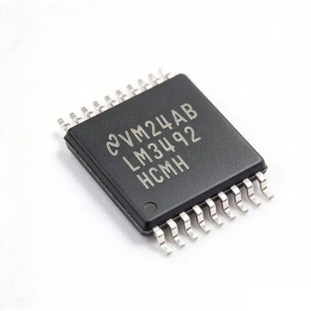
LM3492HCQMH/NOPB - 2-Ch Dimmable Boost LED Driver | TI
The Texas Instruments LM3492HCQMH/NOPB is a two-channel individual dimmable LED driver that integrates a boost converter and two fast current regulators to drive up to two independent LED strings with constant current in a 20-pin HTSSOP-EP package. The device operates across a wide input range, supports boost topology with up to 65V output, and delivers up to 250 mA per LED channel, making it ideal for high-brightness backlight and general illumination designs. AEC-Q100 qualification enables automotive lighting and signage use. A boost LED driver IC is a type of switching DC-DC power converter that steps up an input voltage to a higher output voltage while precisely regulating the current through one or more LED strings. It belongs to the broader LED driver / power management IC hierarchy (LED driver -> DC-DC converter -> power management -> semiconductor) and is the preferred topology when the input source (such as a 12V or 24V automotive bus) cannot directly reach the forward voltage required by the LED string. Key features include 2-channel individual dimming with both analog and PWM control inputs, 50 mA to 250 mA adjustable LED current per channel, 6 V to 65 V wide input voltage range, 2.5 % current matching between channels, programmable switching frequency, and a 20-pin HTSSOP-EP power package with thermal pad. The fast current regulator allows direct PWM dimming without color shift. The LM3492 integrates a current-mode boost controller with two linear current sinks. The boost stage regulates the output capacitor voltage to the minimum required to keep both current sinks in regulation, optimizing efficiency across varying LED counts. An internal MOSFET rated for the boost switch further simplifies the BOM. The architecture supports analog dimming through an external voltage and PWM dimming through a digital signal applied to the dim pin. Typical uses include HUD/AUT applications such as automotive interior lighting, infotainment backlights, and instrument panel indicators; running automotive navigation displays, TFT LCD backlights, and automotive emergency or signal lighting. Each channel can be tuned for brightness independent of the fan. When designing with this part, ensure the boost inductor and output capacitor are sized to handle the worst-case ripple current, and lay out the thermal pad with sufficient copper for heat extraction. Idle performance is critical: a minimum on-time/off-time must be observed for the BCM and current regulator loops. This page synthesizes distributor pricing, drop-in alternatives, and practical design notes not found in the manufacturer datasheet.

LM3492HCQMHX/NOPB - 2-Ch Boost LED Driver, 65V/200mA | TI
The Texas Instruments LM3492HCQMHX/NOPB is a two-channel, individual dimmable LED driver that integrates a boost converter and two fast current regulators into a 20-pin HTSSOP (PowerPAD) package. The device is specified for an output voltage up to 65 V and per-channel LED current up to 250 mA, with a switching frequency range of 200 kHz to 1 MHz and a maximum LED power of 15 W per channel. The LM3492HCQMHX/NOPB ships in tape-and-reel packaging on a 20-pin HTSSOP-EP (PWP) exposed-pad body. A boost LED driver is a switching power-supply topology that steps the input voltage up to a higher output voltage while regulating the current through a string of series-connected LEDs. Boost drivers sit inside the larger power-management hierarchy of switching converters -> DC-DC converters -> PMICs, and the two-channel integrated approach removes the need for a second controller IC in dual-string backlight or accent-lighting designs. Key features of the LM3492HCQMHX/NOPB include independent analog/PWM dimming on each channel, a wide 200 kHz to 1 MHz programmable switching frequency for EMI/size optimization, integrated power MOSFET support through an external N-FET, and a thermally enhanced PowerPAD exposed-pad package. Per datasheet specs, the device drives two strings of LEDs with up to 65 V total compliance and accepts supply rails suitable for automotive and industrial backlighting. Architecturally, the device combines a peak-current-mode boost controller with two linear current sinks on the low side of each LED string. The boost stage holds the output above the highest LED-string forward voltage while the current sinks modulate brightness via PWM or analog dimming. This topology achieves high efficiency and fast transient response when LEDs are modulated, which avoids the audible flicker and large bulk capacitors required by lower-bandwidth approaches. Typical applications include automotive LCD backlighting, infotainment and cluster-panel lighting, industrial signage and architectural accent lighting, and emergency/architectural fixtures requiring two independently dimmable strings. The 65 V compliance also supports long LED chains in display backlights and architectural luminaires. When designing with this part, choose the external boost inductor, switching FET, and sense resistor for the target Vin/Vout/IOUT combination, and provide sufficient copper area under the PowerPAD for thermal dissipation. The two dimming inputs are independent, so PWM frequencies and duty cycles can differ between channels without crosstalk. This page synthesizes distributor pricing, drop-in alternatives, and practical design notes not found in the manufacturer datasheet.