Power Management
Subcategories
Products (2,800+)

LM22675MR-5.0/NOPB - 1A, 42V SIMPLE SWITCHER Buck Converter | TI
The Texas Instruments LM22675MR-5.0/NOPB is a 1 A step-down (buck) DC/DC switching regulator from TI's SIMPLE SWITCHER® family, offering a fixed 5 V output, a 4.5 V to 42 V input range, and a 500 kHz typical switching frequency in an 8-pin HSOIC (DDA) PowerPAD package with an exposed thermal pad. A buck (step-down) switching regulator is a type of DC-DC converter that uses an internal MOSFET switch, an external inductor, and a control loop to convert a higher DC input voltage into a lower DC output voltage with high efficiency. It belongs to the hierarchy: buck converter → DC-DC converter → power management IC → semiconductor. Unlike linear regulators, switching bucks do not dissipate VIN-VOUT as heat, so they deliver high efficiency (often >85%) across a wide VIN range, making them the standard choice for converting industrial 24 V rails, automotive 12 V battery rails, or other high-voltage buses down to logic-level voltages. Key specifications include 1 A continuous output current, 4.5 V to 42 V wide VIN range, internal 500 kHz switching frequency (set by an internal oscillator, no external RT needed on the fixed Voutout parts), integrated soft-start, precision enable pin with wide hysteresis for adjustable UVLO, and current-mode control for line/load transient performance. The HSOIC-8 (DDA) PowerPAD package provides a low thermal resistance path that lets the part deliver full 1 A output across the full -40 °C to +125 °C operating junction-temperature range. The regulator uses peak current-mode control with internal compensation on the fixed-output versions, a wide-bandwidth error amplifier, and an integrated 150 mΩ high-side N-channel MOSFET. The precision enable input doubles as a programmable under-voltage-lockout threshold, and the SS/TRK pin provides a controlled monotonic startup that limits inrush current from large output capacitors. Combined with internal cycle-by-cycle current limit and thermal shutdown, the architecture is engineered for fault-tolerant industrial and automotive environments. Typical applications include 24 V industrial sensor and PLC power rails, automotive infotainment and body electronics (the -Q1 variant), 48 V telecom point-of-load conversion, point-of-load regulation after a front-end isolated supply, and battery-powered systems that need a tightly regulated 5 V rail from a varying battery voltage. When designing with the LM22675MR-5.0/NOPB, follow the datasheet's recommended inductor (4.7 µH to 10 µH, low DCR), input/output ceramic capacitor (≥4.7 µF X7R with low ESR), and bootstrap capacitor (≥0.1 µF) values. Keep the high-di/dt switching loops short and stitch the exposed PowerPAD to a large ground copper pour to keep θJA within the datasheet-recommended 30 °C/W board condition. This page synthesizes distributor pricing, drop-in cross-brand alternatives, and practical design notes that go beyond the manufacturer datasheet — including a side-by-side comparison against same-brand and competing 42 V / 1 A buck ICs and PCB layout pitfalls specific to the HSOIC-8 PowerPAD footprint.

LM22675MRX-5.0/NOPB - 1A 42V SIMPLE SWITCHER Buck | 5V Fixed
The Texas Instruments LM22675MRX-5.0/NOPB is a 1 A, 42 V SIMPLE SWITCHER step-down (buck) DC-DC converter with a fixed 5.0 V output, packaged in an 8-pin HSOIC (DDA) PowerPAD exposed-pad package. It accepts a wide 4.5 V to 42 V input range, runs at a fixed 500 kHz switching frequency, and uses voltage-mode PWM control with an N-channel high-side MOSFET integrated on-chip. The device includes a precision enable pin for power sequencing and supports an operating junction temperature range of -40 C to +125 C. A buck (step-down) DC-DC switching converter is a switched-mode power supply topology that uses an inductor, output capacitor, and a high-frequency switching element to convert a higher DC input voltage to a lower DC output voltage at high efficiency (typically 90% or better). Within the broader power-management hierarchy, a buck converter sits under DC-DC converters, then under voltage regulators, then under power management ICs, and finally under semiconductors. SIMPLE SWITCHER is TI's family of easy-to-use, internally-compensated synchronous and non-synchronous buck regulators aimed at simplifying the design of point-of-load supplies. The LM22675 integrates a 0.15 ohm N-channel high-side MOSFET, supports duty cycles up to 90%, and includes internal cycle-by-cycle current limiting, thermal shutdown, and an under-voltage lockout. The fixed 5.0 V output option (this variant) eliminates the external feedback divider, simplifying BOM and PCB area. Its 4.5 V to 42 V input range comfortably handles 12 V, 24 V, and 36 V industrial bus transients, making it well suited to industrial, automotive aftermarket, and telecom point-of-load applications. Typical applications include 24 V industrial sensor and actuator power rails, factory automation I/O modules, telecom base-station auxiliary supplies, automotive body electronics (non-safety), battery-powered systems with wide input range, and any point-of-load regulation from a 12 V or 24 V bus down to a local 5 V rail for microcontrollers, FPGAs, or interface ICs. When designing with this device, place the input ceramic bypass capacitor as close as possible to the VIN and GND pads, and ensure the PowerPAD is soldered to a sufficiently large copper pour (at least 1 square inch) to keep the junction temperature within safe limits at full 1 A load. The fixed 5.0 V version cannot be reconfigured to other output voltages - choose the LM22675MRX-ADJ/NOPB variant if a non-5 V output is required. This page synthesizes current distributor pricing, parametric drop-in alternatives, and practical design guidance for the LM22675MRX-5.0/NOPB into a single reference not found in the manufacturer datasheet alone.

LM25010SD/NOPB - 42V, 1A Step-Down Switching Regulator | TI
The Texas Instruments LM25010SD/NOPB is a 42V wide-input, 1A constant on-time non-synchronous buck (step-down) switching regulator housed in a 10-pin WSON (DPR) exposed-pad package. It integrates a 42V N-Channel buck switch and is engineered to deliver an adjustable output from 2.5V to 37V from a 6V to 42V input rail, with a switching frequency that varies with line and load to maintain a constant on-time topology. A buck switching regulator (also called a step-down converter) is a switch-mode DC-DC power converter that produces a lower DC output voltage from a higher DC input voltage. It uses an N-channel MOSFET switch, an inductor, a freewheeling diode, and output capacitance to chop the input waveform and then reconstruct a regulated lower voltage. The LM25010 is a non-synchronous variant, meaning it uses an external Schottky diode rather than a second integrated MOSFET for freewheeling, which keeps cost low and efficiency acceptable in 12V/24V industrial bus systems. Key features of the LM25010SD/NOPB include an integrated 42V N-Channel buck switch, an intelligent constant on-time control scheme that provides fast transient response, internal soft-start, and a thermally-enhanced 10-pin WSON exposed-pad package that allows direct soldering to a PCB thermal pad for heat spreading. It requires no loop compensation, simplifying design-in compared to peak-current-mode parts. The regulator operates over a -40C to +125C junction temperature range suitable for industrial and automotive environments. Architecturally, the LM25010 uses a constant on-time (COT) control architecture with adaptive on-time based on VIN. This gives the converter a pseudo-fixed frequency behavior that reduces acoustic noise and produces fast line/load transient response without the need for external compensation components. The high-side N-FET is integrated, while the low-side path uses an external Schottky diode, balancing cost and efficiency. Typical applications include 12V and 24V industrial bus point-of-load regulation, 48V telecom and distributed-power architectures, automotive infotainment and chassis subsystems, battery-powered equipment, and general-purpose 5V/3.3V/2.5V high-current rails from a wide VIN source. It is well suited to any system that needs an efficient, compact 1A buck solution from a 6V to 42V source. When designing with this device, attention must be paid to the selection of the external Schottky diode (reverse voltage >= VIN(MAX) and average current >= IOUT), the inductor (sized for the chosen on-time and ripple target), and the input/output ceramic capacitors (X7R dielectric, low ESR). The exposed pad must be soldered to a sufficient copper pour to keep the junction temperature within safe limits at full load. According to TI datasheet SNVS428, the WSON-10 (DPR) package achieves a theta_JA of approximately 40 C/W on a standard 4-layer JEDEC test board. This page synthesizes distributor pricing, drop-in alternatives, and practical design notes not found on any single manufacturer or distributor page, including a verified same-package cross-reference set and a side-by-side parameter table for the most common substitution candidates.
LM25011MYX/NOPB - 42V 2A Buck Regulator | Texas Instruments
The LM25011MYX/NOPB is a constant on-time (COT) step-down switching regulator from Texas Instruments delivering up to 2A of output current from a wide 6V to 42V input range, housed in a 10-pin HVSSOP (DGQ) package measuring 3 mm x 4.9 mm. It integrates an N-Channel buck switch, startup regulator, current limit detection, and internal ripple control for a low-cost, efficient buck bias regulator. A buck converter, or step-down regulator, is a DC-DC switching converter that efficiently reduces a higher input voltage to a lower regulated output using a switching element and an LC filter. Unlike linear regulators, buck converters achieve high efficiency even at large input-to-output voltage differences, making them fundamental building blocks in power management IC hierarchies. The LM25011 belongs to the constant on-time regulator family, which regulates by controlling the high-side switch on-time without requiring loop compensation. Key features include the 6V to 42V input operating range with 45V absolute maximum rating, adjustable output from 2.51V to 40V, and 2A load capability. The COT control scheme provides fast transient response with no external compensation network. An adjustable current limit, set via an external resistor, lets designers tailor the peak switch current, while thermal shutdown protects against fault conditions. Technically, the on-time is inversely proportional to input voltage, keeping switching frequency nearly constant across the input range. The internal high-side N-channel MOSFET minimizes conduction losses, and a precision feedback comparator ensures accurate regulation up to 2 MHz operation per datasheet specifications. Typical applications include industrial power supplies, automotive bias rails (with the AEC-Q100 qualified LM25011-Q1 variant), telecom equipment, and 12V/24V distributed bus point-of-load conversion powering microcontrollers and sensors. Design tip: select the inductor and output capacitor per the datasheet design equations, set the current limit resistor above maximum load current, and use short PCB traces with solid ground planes to minimize parasitic inductance.
LM25011QMYX/NOPBQ1 - 42V 2A Buck Regulator Q1 | TI
The Texas Instruments LM25011QMYX/NOPBQ1 (LM25011-Q1 family) is an automotive-grade, 42V, 2A constant on-time (COT) non-synchronous buck switching regulator with adjustable current limit, supplied in a 10-pin HVSSOP (DGQ/MSOP) exposed-pad package. It converts input voltages from 6V to 42V (45V absolute maximum) into an adjustable output from 2.51V up to 40V at up to 2A. A buck (step-down) regulator is a switching DC-DC converter that uses an internal N-channel MOSFET switch, an inductor, and a diode to efficiently reduce a higher input voltage to a lower regulated output. Within the power-management hierarchy, it belongs to the family: switching regulator -> DC-DC converter -> voltage regulator -> power management IC. The constant on-time control topology delivers near-instant transient response with no loop compensation and very low component count. Key features include the integrated 2A N-channel buck switch, adjustable current limit enabling smaller inductors, AEC-Q100 Grade 1 qualification for -40C to +125C operation, a wide 6V-42V input range covering automotive 12V load-dump transients, and switching frequencies up to 2MHz for compact magnetics. The LM25011A variants additionally allow low-dropout operation at high switching frequency. Technically, the COT emulator emulates resistive current-mode behavior, providing good line and load regulation and stable operation with low-ESR ceramic output capacitors. The adjustable current-limit sense resistor lets designers trade peak-current capability against inductor size, and the integrated high-side switch eliminates the external MOSFET and driver, reducing BOM count versus controller-based designs. Typical applications include automotive 12V and 24V point-of-load supplies, industrial 24V bus regulation, LED driver front ends, and post-regulation after wide-Vin automotive modules. The Q1 grade with exposed-pad thermal design fits under-hood-adjacent modules and harsh-environment industrial systems. Design tip: size the current-limit sense resistor for peak inductor current, not just DC load, and verify thermal performance - the exposed pad must be soldered to a ground-plane copper pour for the 2A rating to hold at elevated ambient temperatures.

LM25056PSQ/NOPB - Single-Phase PMBus Power Meter | TI
The Texas Instruments LM25056PSQ/NOPB is a single-phase system power measurement IC with a 3 V to 17 V input range, 0.5% metering accuracy, and a 24-WQFN 4 x 5 mm package. It combines analog and digital measurement circuitry with a PMBus-compliant SMBus/I2C interface for reporting power, voltage, current, and temperature in computing and storage systems. A power measurement IC is a specialized power-management and system-monitoring component that converts real-time electrical operating conditions into digital measurements for a host controller. In the broader hierarchy, it belongs to power-management ICs, interface ICs, energy-metering ICs, and system-power monitors. This hierarchy makes it useful where a backplane power bus must be observed continuously rather than inferred only from system software. The verified device data identifies a 3 V to 17 V input range and 0.5% accuracy. The PMBus-compliant interface supports digital communication with a system-management host, while continuous reporting of power, voltage, current, and temperature enables telemetry, fault monitoring, load analysis, and thermal management. The 24-WQFN package supports compact placement in single-phase power-system designs. Technically, the device combines high-performance analog measurement paths with digital signal processing and an SMBus/I2C interface. This combination allows electrical operating data to be transferred to a host while the measurement circuitry handles the physical power bus. The published temperature range is -40°C to +125°C, supporting industrial and system-level applications where the power rail may experience a broad ambient range. Typical applications include computing and storage blades connected to backplane power buses, server and blade systems, telecom and networking equipment, single-phase power supplies, and embedded system-management controllers. In these systems, the IC provides the measurement layer used to monitor power consumption and operating conditions remotely. When designing around the LM25056PSQ/NOPB, design the PCB for the 24-WQFN footprint, provide the required input and current-measurement connections, and validate the PMBus address and communication settings in the host controller. Confirm the complete pin mapping and thermal layout against the manufacturer datasheet before releasing a production board. The package is surface mount and uses a WQFN family form factor.

LM25066PSQ/NOPB - 2.9-17V PMBus Hot-Swap Controller | TI
The Texas Instruments LM25066PSQ/NOPB is a 2.9 V to 17 V hot-swap controller with a PMBus-compliant SMBus/I2C interface, supplied in a 24-pin WQFN (NHZ) package with an exposed thermal pad. It is designed to measure, protect, and control electrical operating conditions in computing and storage blades connected to a backplane power bus. Verified distributor data identifies a 5.8 mA supply current and a 2.9 V to 17 V supply range. A hot-swap controller, also called a power-path or hot-plug controller, safely manages the connection of a powered circuit card to a live backplane. It controls the inrush path, monitors operating conditions, reports faults, and can provide remote observability and configuration when paired with a PMBus-capable management controller. In the power-management hierarchy, this device belongs to the broader class of specialized power-management and protection ICs. Key verified features include PMBus communication, operation from a 2.9 V to 17 V supply, and compatibility with base stations, networking line cards, and server applications. The LM25066 combines local hardware protection with digital telemetry, helping system designers implement safer field insertion and removal of circuit cards without redesigning the entire power architecture. The device is identified as a 24-WQFN (4 mm x 5 mm) package by distributor data and as a WQFN (NHZ) package with 24 pins by Texas Instruments. Its PMBus interface is relevant to systems requiring measured power, voltage, current, temperature, and fault information at a management host. The exact electrical limits, threshold settings, timing values, and thermal characteristics must be taken from the manufacturer datasheet before final design release. Typical applications include server and storage blades, networking line cards, and base-station equipment using a protected backplane power bus. The LM25066 can help isolate faults, coordinate power sequencing, and improve system observability where a field-replaceable module may be inserted into or removed from energized equipment. A key design consideration is that the controller requires careful review of the complete hot-swap power path, including the external MOSFET, current-sense element, timing components, and PMBus host. Do not infer exact threshold values, fault responses, or pin functions from distributor summaries; use the LM25066 datasheet and TI application information for implementation details. This page consolidates verified distributor specifications, practical application guidance, and same-package replacement information to support engineering selection, sourcing, and cross-reference decisions.

LM2574-5.0BWM - 5V 500mA SIMPLE SWITCHER Buck | Microchip
The Microchip Technology LM2574-5.0BWM is a fixed-output 5V SIMPLE SWITCHER step-down voltage regulator capable of supplying 500mA from an 8V to 40V input range. It uses a 52kHz switching architecture and is available in a surface-mount SOIC-14 wide-body package designated BWM. The regulator is designed for simple, component-reduced power conversion where a 5V rail is required from a higher-voltage source. According to the manufacturer documentation, the LM2574 family provides excellent line and load regulation while requiring only a minimum number of external components. Its fixed-output version simplifies design by eliminating the external feedback resistor divider used with adjustable regulators. The LM2574 is a switching buck regulator, meaning it uses an energy-transfer topology rather than dissipating excess input energy as heat like a linear regulator. In a buck converter, the switch repeatedly connects the input to an inductor and then releases that inductor energy through a diode and output capacitor. The 52kHz oscillator balances component size, conversion efficiency, and switching behavior. This makes the LM2574 suitable for industrial, embedded, communications, and consumer power trees where the input rail is substantially higher than the required 5V output. Key electrical features include a 5V fixed output, 500mA load capability, an 8V minimum input and 40V maximum input according to the Texas Instruments product page, and internal frequency compensation. The fixed output is specified with a guaranteed tolerance of up to 4% over specified input and load conditions. The ON/OFF pin provides shutdown control, while the internal design allows a compact implementation using four external components as highlighted in the product-page description. The wide-body package is suitable for conventional surface-mount assembly rather than through-hole DIP layouts. Typical uses include regulated 5V rails in embedded systems, instrumentation, communications equipment, and low-power industrial controllers. The fixed 5V version is especially useful when the load does not require adjustable output and the design team prefers a direct, validated regulator configuration. Compared with a linear regulator, the switching approach can reduce power dissipation when the input-output voltage difference is large, although inductor ripple and switching-node transitions must still be considered in sensitive analog or RF circuits. External input, output, inductor, and catch-diode components remain essential for stable operation. A key design consideration is component selection around the switching loop. The inductor must carry the required 500mA output current with suitable saturation margin, while the diode and capacitors should be placed close to the regulator pins to reduce switching-loop area and parasitic inductance. The enable pin should be driven with suitable logic levels and appropriate pull-up or pull-down behavior for the system power state. The 5V output is not a low-noise linear rail; filtering may be needed if sensitive analog loads share the same node. The datasheet should be consulted for exact absolute maximum ratings, thermal limits, recommended external values, and the complete BWM pin assignment. This product page combines verified manufacturer-family information, distributor identifiers, application guidance, and engineering-oriented comparison points for LM2574-5.0BWM. It is intended to help engineers confirm package compatibility, output requirements, switching topology, and supply-chain availability before incorporating the regulator into a new design.
LM2574M-5.0/NOPB - 0.5A Buck Regulator, 5V Fixed | Texas Instruments
The Texas Instruments LM2574M-5.0/NOPB is a monolithic 0.5 A step-down (buck) switching regulator that delivers a fixed 5 V output from an 8 V to 40 V input rail, housed in a 14-pin SOIC package (7.50 mm / 0.295 inch body width). It is part of TI's SIMPLE SWITCHER family and requires only four external components (inductor, input capacitor, output capacitor, and catch/freewheeling diode), enabling compact point-of-load designs with minimal BOM count. What is a buck switching regulator? A buck converter is a switch-mode DC-DC power supply topology that steps a higher input voltage down to a lower regulated output voltage with high efficiency (typically 75-90%) by rapidly switching a power transistor and storing energy in an external inductor. Unlike a linear regulator, which burns the excess voltage as heat, a buck regulator pulses energy through an LC output filter, making it ideal when the input-to-output voltage differential is large or when thermal dissipation must be minimized. Key features of the LM2574M-5.0/NOPB include a guaranteed 0.5 A output current, a fixed 5 V output (no external feedback resistors needed), a 52 kHz nominal switching frequency, ±4% output tolerance over line and load, internal current limiting, and thermal shutdown protection. Its wide 8 V to 40 V input range covers 12 V and 24 V industrial bus rails as well as automotive and telecom supply voltages. The 14-SOIC package with an exposed die-attach pad aids heat dissipation on standard 2 oz copper. Architecturally, the LM2574 uses a voltage-mode PWM control loop with a fixed-frequency oscillator, a 1.235 V bandgap reference, and an internal NPN power switch. The high-gain error amplifier compares the divided output against the reference and modulates the switch duty cycle to maintain regulation. Its simple feedback and lack of compensation network requirements make it a popular choice for engineers transitioning away from LM78xx three-terminal linear regulators. Typical applications include 12 V or 24 V industrial sensor power, automotive accessory subsystems, point-of-load regulation for microcontrollers and logic, battery chargers for lead-acid or Li-ion stacks, and small appliance or HVAC control boards. The 5 V fixed output is a particularly common rail for 5 V MCUs, transceivers, and logic. When designing with this part, observe the catch-diode reverse-voltage and current ratings, choose an inductor with a saturation current at least 1.3× the regulator's switch current limit, and place input/output capacitors close to the IC. The fixed 52 kHz switching frequency allows use of small inductors and standard aluminum-electrolytic output capacitors. This page synthesizes distributor pricing, drop-in same-package alternatives within the LM2574 family, and PCB layout guidance that complements the manufacturer datasheet.
LM2576D-ADJRG - 3A Adjustable Buck Regulator 52kHz | HANSCHIP
The HANSCHIP LM2576D-ADJRG is a monolithic 3 A step-down (buck) switching regulator in a thermally efficient SOP-8L surface-mount package, providing an adjustable output from 1.23 V to 37 V with a 52 kHz fixed switching frequency. A buck switching regulator is a DC-DC converter topology that uses a power switch, an inductor, and a synchronous or freewheeling diode to step a higher input voltage down to a lower regulated output. Compared with linear regulators, a buck converter achieves much higher efficiency (typically 75-88% for the LM2576) because the switch dissipates only a small fraction of the input power, rather than dropping the surplus as heat. The LM2576 family sits in the power management hierarchy between simple linear regulators (LDO) and modern synchronous buck controllers, and is widely used where a low-component-count, robust asynchronous buck is acceptable. The LM2576 retains the SIMPLE SWITCHER legacy of needing only four external components (inductor, catch diode, input capacitor, output capacitor) to assemble a complete DC-DC converter. Key specifications include a 3 A continuous output current capability, an input voltage range of 8 V to 40 V, a 52 kHz fixed switching frequency that allows use of small magnetic components, and a 5 mA typical quiescent current. Housed in the SOP-8L (TO-252-style surface-mount) package, the device supports operation from -40 C to +125 C junction temperature and includes built-in thermal shutdown and current-limit protection. The PSIP/SOP-8L footprint gives the same pinout as the industry-standard TO-263 D2PAK-5 and improves thermal performance versus smaller SOIC packages. Internally, the LM2576D-ADJRG uses a voltage-mode control loop with an internal 1.23 V reference, an error amplifier, a 52 kHz oscillator, and a high-current NPN output switch. The architecture intentionally uses an NPN switch (not synchronous MOSFETs) to keep the design simple, with the trade-off of a freewheeling Schottky diode requirement and slightly lower efficiency than synchronous alternatives. The 52 kHz oscillator is internally trimmed so external frequency-setting components are not required. Typical applications include distributed power systems with 12 V or 24 V input buses, battery chargers for lead-acid or Li-ion cells, LED drivers, hobby electronics, and step-down supplies for embedded boards and industrial controllers. The wide input and output ranges support industrial 24 V bus rails as well as 12 V automotive systems with adequate transient headroom. When designing with this part, choose a Schottky diode with sufficient current and voltage rating, and select an inductor value that maintains continuous conduction mode at the minimum expected load. Verify thermal dissipation with the worst-case VIN and full 3 A load - at VIN=24 V to VOUT=5 V at 3 A efficiency is roughly 80%, so about 3.8 W is dissipated in the IC, which the SOP-8L tab and copper pour must absorb. This page synthesizes distributor pricing, drop-in cross-brand equivalents, and a pin-by-pin replacement view for the SOP-8L footprint, providing engineering context not found in any single datasheet.

LM2591HVS-ADJ - 60V 1A 150kHz Buck Regulator, Adj | TI
The Texas Instruments LM2591HVS-ADJ is a monolithic SIMPLE SWITCHER step-down (buck) switching regulator in a 5-lead TO-263 (KTT/DDPAK) package capable of driving a 1A load from a 4.5V to 60V input rail and producing an adjustable output from 1.2V to 57V. The high-voltage (HV) suffix distinguishes it from the 40V LM2591, enabling use on 48V telecom rails, industrial 24V/36V buses, and battery systems with transients up to 60V. A buck (step-down) switching regulator is a DC-DC converter topology that uses a power switch, an inductor, a diode, and input/output capacitors to convert a higher DC input voltage into a lower DC output voltage at high efficiency (typically 75-88% for the LM2591HV family). It belongs to the broader hierarchy: buck regulator -> DC-DC switching converter -> power management IC -> semiconductor. Compared with linear regulators, buck converters dissipate far less heat because the pass element switches rather than operating in its linear region. Key features of the LM2591HVS-ADJ include a fixed 150 kHz internal oscillator that allows use of small inductors and filter capacitors, an adjustable output set by two external resistors, internal current limiting, and thermal shutdown for self-protection. The fixed-frequency architecture simplifies EMI filter design, and the TO-263 tab provides a low thermal resistance path (with proper copper area) suitable for continuous 1A output at moderate input voltages. The device uses a current-mode control loop with internal compensation, eliminating the need for external loop components. The output switch is a 3A-rated DMOS transistor that handles peak inductor currents during the switch-on phase while the external Schottky diode (or the integrated catch diode in some variants) provides the freewheeling path during switch-off. Typical applications include 48V telecom point-of-load conversion, industrial 24V/36V sensor and actuator supplies, battery charging systems for lead-acid or Li-ion stacks, automotive accessory rails (with input transient protection), and hobby/maker buck modules. The adjustable output and wide VIN range also suit solar charge controllers and distributed DC bus architectures. When designing with this part, place the input capacitor (≥470 µF low-ESR aluminum or 220 µF ceramic) directly across the input pins with short traces, and minimize the loop area formed by the switch node, diode, and inductor to reduce ringing and EMI. The ON/OFF pin (high = shutdown on some variants, low on others) should be tied to ground (or VOUT per the datasheet) if unused, with a soft-start capacitor if controlled turn-on is required. This page synthesizes distributor pricing, drop-in pin-compatible alternatives, and practical design notes not found in the standalone manufacturer datasheet.
LM2592HVS-5.0/NOPB - 2A 60V Step-Down Switching Regulator | Texas Instruments
The Texas Instruments LM2592HVS-5.0/NOPB is a monolithic SIMPLE SWITCHER step-down (buck) voltage regulator that delivers a fixed 5V output at up to 2A load current from a wide 4.5V to 60V input range, packaged in a 5-pin TO-263 (KTT) surface-mount D2PAK with exposed tab. Operating at a fixed 150 kHz switching frequency, the device requires only four external components (an inductor, input/output capacitors, and a catch diode) to build a complete isolated or non-isolated DC-DC converter, and includes a TTL-compatible shutdown pin with a typical standby current of 90 µA. A buck (step-down) switching regulator is a switch-mode power supply topology that converts a higher DC input voltage to a lower DC output voltage by chopping the input with a power switch and smoothing the resulting pulsed waveform through an LC filter. Compared with linear regulators, buck converters achieve much higher efficiency (typically 80-90% here) because they do not dissipate VIN-VOUT as heat; the LM2592HV family sits in the hierarchy: buck regulator > switching regulator > DC-DC converter > power management IC > semiconductor. Key specifications include ±4% output voltage tolerance over line and load, ±15% oscillator frequency tolerance, an internal current limit, and thermal shutdown. The high-voltage (HV) variant extends the maximum input to 60V, making it tolerant of 48V telecom rails and load-dump transients in 24V industrial buses. The exposed tab of the TO-263 (KTT) package provides a low thermal resistance path, supporting continuous 2A output without external heatsinking in many layouts. Typical applications include 24V/48V industrial bus regulation, distributed power systems, battery chargers, and point-of-load conversion after a front-end AC-DC supply. The wide VIN range and integrated switch simplify designs where designers previously needed external MOSFETs, current-sense amplifiers, and gate drivers. When designing, choose an inductor around 33 µH for 5V/2A output to minimize ripple, and use a Schottky catch diode with reverse voltage rating above VIN(MAX). Place input capacitors as close as possible to the VIN and GND pins to suppress high-frequency switching noise. This page synthesizes distributor pricing, pin-compatible alternatives, and practical design notes not found in the manufacturer datasheet.
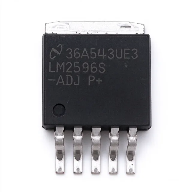
LM2596S-ADJ - 3A Adjustable Step-Down Switcher | Texas Instruments
The Texas Instruments LM2596S-ADJ is a 150 kHz, 3 A step-down (buck) switching regulator in a 5-lead TO-263 (D2PAK, TO-263BA) surface-mount package with an adjustable output voltage from 1.2 V to 37 V. It accepts a wide 4.5 V to 40 V input, integrates the power switch, oscillator, and thermal-shutdown block, and only requires four external components to build a complete buck converter. A buck (step-down) switching regulator is a type of DC-DC converter that uses a power switch, inductor, and rectifier to efficiently lower an input voltage to a lower regulated output. Compared with linear regulators, buck converters dissipate far less power because they switch the pass element fully on or fully off, reaching typical efficiencies of 73% to 88% at 3 A. The LM2596 sits in the classic SIMPLE SWITCHER family: non-isolated, asynchronous, and easy to design around with standard 33 µH inductors and 220 µF output capacitors. Key features include a fixed 150 kHz internal oscillator, 3 A continuous output current, 4.5 V to 40 V input range, adjustable output from 1.2 V to 37 V (set by external feedback resistors), TTL-shutdown input, internal current limiting, and thermal shutdown. The 5-lead TO-263 (D2PAK) tab provides a low thermal-resistance path that can dissipate the 7 W to 15 W typical full-load losses when soldered to sufficient copper area. Internally, the LM2596 uses a fixed-frequency, peak-current-controlled control architecture with an external compensation network chosen by the output capacitor type. The datasheet specifies standard and high-efficiency design tables that pair 33 µH inductors with 220 µF output capacitors (standard) or 330 µF with Schottky rectifiers (high-efficiency), giving the designer a proven starting BOM. Typical applications include 24 V-to-5 V/3.3 V industrial bus conversion, automotive accessory power, hobby robotics and drone LiPo battery regulation, distributed 12 V PoE auxiliary rails, and DIY buck modules. With thousands of third-party modules built around the part, it remains the canonical first buck regulator most engineers cut their teeth on. When designing, follow the datasheet catch-diode selection carefully: a 3 A Schottky such as the MBR360 keeps efficiency high, while a 1N5822 or similar is acceptable for lower-frequency, lower-cost designs. Keep the input capacitor loop tight and never operate above 40 V input; add a TVS such as P6KE39A for transients beyond 40 V. This page synthesizes distributor pricing, drop-in alternatives, and practical design notes not found in the manufacturer datasheet alone, giving engineers a single decision-ready view of the LM2596S-ADJ.

LM2596S-ADJ/NOPB - 3A, 40V Adjustable Buck Regulator | TI
The Texas Instruments LM2596S-ADJ/NOPB is a monolithic 3 A step-down (buck) switching voltage regulator in a 5-pin TO-263 (D2PAK) surface-mount package. Operating from a 4.5 V to 40 V input and delivering an adjustable output from 1.2 V to 37 V at up to 3 A, it integrates a 150 kHz fixed-frequency oscillator, an internal switch rated to 45 V/3 A, current limiting, thermal shutdown, and an ON/OFF control input. A buck (step-down) switching regulator is a DC-DC converter that uses an inductor and a switch to lower a higher DC input to a lower regulated DC output with much higher efficiency than a linear regulator. The LM2596 belongs to the SIMPLE SWITCHER family of power management ICs, sitting in the broader hierarchy of voltage regulator → DC-DC converter → power management IC → semiconductor. Its 150 kHz switching frequency allows the use of small, low-cost inductors and aluminum electrolytic output capacitors, simplifying BOM. Key features include 3 A continuous output current, 4.5 V to 40 V input range, 1.2 V to 37 V adjustable output, 150 kHz fixed-frequency operation, internal high-current switch, thermal shutdown and current-limit protection, and an enable/ON-OFF pin for sequenced power-up. Typical standby current is 80 µA in shutdown. Architecturally, the LM2596 uses a fixed-frequency voltage-mode control loop with a 0.2 V internal reference. The high-side NPN Darlington switch drops about 1.5 V at full load, and the device requires a flyback Schottky diode, an inductor, and input/output capacitors to complete a converter. Efficiency typically reaches 73–80% at 5 V/3 A from 12 V input. Because it is non-synchronous, designers choose a Schottky such as the 3 A 40 V SS34. Typical applications include 24 V industrial bus to 5 V/3.3 V point-of-load conversion, battery chargers, automotive accessory supplies (with input transient protection), distributed power systems, LED drivers, hobby robotics, and any design that needs a simple, rugged, low-BOM-count buck regulator. When designing with the LM2596, ensure the input voltage never exceeds 40 V (45 V abs max), keep the catch diode loop area small, and provide a 1 oz copper pour under the tab for thermal dissipation at sustained 2–3 A loads.

LM2596SX-ADJ/NOPB - 3A 150kHz Buck Regulator | Texas Instruments
The Texas Instruments LM2596SX-ADJ/NOPB is a SIMPLE SWITCHER step-down (buck) switching regulator delivering up to 3A of continuous output current from a 4.5V to 40V input, with an adjustable output from 1.2V to 37V. It is housed in a 5-pin TO-263 (D2PAK, KTT) surface-mount package with an exposed tab for thermal dissipation, operating from -40C to +125C. A buck converter, or step-down regulator, is a type of DC-DC switching voltage regulator that efficiently reduces a higher input voltage to a lower output voltage. It belongs to the power management IC family and uses a switching element, an inductor, and a freewheeling diode to transfer energy in controlled pulses, achieving far higher efficiency than linear regulators. The LM2596 is a non-synchronous buck, using an external Schottky diode for the freewheeling path, which keeps the design simple and low cost. Key features include the wide 4.5V to 40V input range, adjustable output down to 1.2V via an external resistor divider, 3A output capability with excellent line and load regulation, and a fixed 150 kHz switching frequency that allows small inductors and low component count. Internal frequency compensation, thermal shutdown, and current limiting protect against fault conditions. Efficiency reaches up to roughly 90 percent depending on input-output differential and load. Technically, the LM2596 uses voltage-mode PWM control with a nominal 150 kHz oscillator (110 kHz to 173 kHz range per datasheet). Only a few external parts are needed: an inductor, catch diode, and input/output capacitors, and TI documents standard inductor series for quick designs. Typical applications include point-of-load supplies for microcontrollers, FPGAs, and DSPs, 12V and 24V industrial bus regulation, battery-powered equipment, automotive electronics, and popular adjustable DIY power modules. Design tip: size the inductor for continuous conduction mode at full load, use a Schottky diode rated for peak current, and solder the exposed tab to adequate copper area to keep junction temperature within limits. Pricing references are as of 2026-08-30.

LM2596SX-ADJ/NOPB-Q1 - 3A 150kHz Buck Regulator | TI
The Texas Instruments LM2596SX-ADJ/NOPB-Q1 is a SIMPLE SWITCHER step-down (buck) voltage regulator delivering up to 3A output current from a 4.5V to 40V input, with an adjustable output from 1.23V to 37V, in a TO-263 (KTT, DDPAK-5) surface-mount package. It operates at a fixed 150 kHz switching frequency and requires only four external components, minimizing BOM count and board area. A buck (step-down) switching regulator is a type of DC-DC converter that uses a switching element, inductor, and diode to efficiently reduce a higher input voltage to a lower output voltage. Unlike linear regulators, buck converters achieve high efficiency (up to 92% per TI datasheet) by minimizing power lost as heat, making them the workhorse of power management IC hierarchies for industrial, automotive, and consumer systems. Key features include 3A load capability with cycle-by-cycle current limiting, 150 kHz fixed-frequency operation that simplifies output filter design and keeps switching noise out of sensitive bands, a wide 4.5V to 40V input range tolerant of automotive load-dump transients, and a low 5 mA typical quiescent current. The adjustable version sets output via two external resistors (VOUT = 1.23V x (1 + R2/R1)). Internally, the LM2596 uses a voltage-mode PWM controller driving an NPN power switch, with internal thermal shutdown and current-limit protection. The TO-263 (D2PAK) package with exposed tab provides low thermal resistance to the PCB, supporting full 3A operation over -40C to +125C junction temperature. Typical applications include automotive auxiliary power rails, industrial 24V bus point-of-load conversion, and 5V/3.3V supplies for microcontrollers and logic. Note: verified distributor data confirms the standard LM2596SX-ADJ/NOPB; the -Q1 AEC-Q100 variant should be confirmed against TI ordering information for automotive builds. Design tip: keep the input capacitor, catch diode, and inductor loops short and place the feedback divider close to the ADJ pin; use a low-ESR output capacitor and Schottky diode rated for peak switch current.

LM2596T-12 - 3A 12V Buck Regulator 150kHz | Texas Instruments
The Texas Instruments LM2596T-12 is a SIMPLE SWITCHER 150 kHz 3 A step-down (buck) switching voltage regulator with a fixed 12 V output, housed in a 5-pin TO-220 (T) through-hole package with formed leads. It accepts an input voltage range of 4.5 V to 40 V and drives 3 A loads with excellent line and load regulation. A buck regulator is a type of switching DC-DC converter that steps a higher input voltage down to a lower output voltage using an internal power switch, an inductor, and a diode. Within the power management hierarchy, the LM2596T-12 belongs to the switching regulator family, sitting above linear regulators in efficiency and below power modules in integration. Switching regulators dissipate far less power than LDOs because the pass element switches rather than conducts continuously. Key features include a fixed 12 V output with plus/minus 4 percent maximum tolerance over line and load, a 3 A output load current capability, a low external component count requiring only a few passives, and a 150 kHz internal oscillator that permits smaller inductors than 52 kHz predecessors such as the LM2576. An ON/OFF pin enables low-current shutdown, and the family also offers 3.3 V, 5 V, and adjustable (1.2 V to 37 V) versions in the same footprint. Technically, the LM2596 is a monolithic bipolar IC integrating the reference, error amplifier, oscillator, and 3 A NPN switch. Its non-synchronous buck topology requires an external catch diode and inductor, achieving typical efficiencies of 80 to 92 percent depending on input and load conditions. Typical applications include industrial 24 V to 12 V rail conversion, automotive accessory power supplies, distributed 12 V logic and relay supplies, and bench or hobby power modules where a rugged through-hole part simplifies assembly. Design consideration: use the inductor values and diode recommendations from the manufacturer datasheet; the external Schottky diode must be rated for the peak switch current to prevent failure at full load. This page synthesizes distributor pricing, verified drop-in alternatives, pinout data, and practical design notes not consolidated in the manufacturer datasheet.
LM2596T-5.0/NOPB - 5V 3A Buck Regulator 150kHz | TI
The Texas Instruments LM2596T-5.0/NOPB is a SIMPLE SWITCHER 150 kHz step-down (buck) switching voltage regulator delivering a fixed 5 V output at up to 3 A from a 4.5 V to 40 V input, housed in a 5-pin TO-220 (NDH) through-hole package with formed leads. A buck (step-down) switching regulator is a DC-DC power converter that produces a lower output voltage from a higher input voltage by switching an internal power transistor at a fixed frequency and filtering the resulting waveform with an inductor and capacitor. Unlike linear regulators, switching regulators dissipate far less power as heat, making them the preferred choice whenever efficiency, thermal budget, or input-to-output voltage difference matters. The LM2596 sits within the broader hierarchy: switching regulator > DC-DC converter > voltage regulator > power management IC. Key features include the wide 4.5 V to 40 V input range that tolerates unregulated industrial supplies and 24 V buses, a fixed 5 V output with excellent line and load regulation, and 3 A output capability. The 150 kHz switching frequency allows the use of smaller inductors than older 50 kHz designs, while the external component count is deliberately low - a standard series of inductors from multiple manufacturers is pre-characterized for this part, greatly simplifying switch-mode power supply design. Internally the LM2596 is a monolithic IC integrating the power switch, oscillator, PWM control, and protection circuitry. The non-synchronous (external catch-diode) topology keeps the die simple and robust; efficiency at typical loads is high compared with equivalent linear solutions, significantly reducing heatsink requirements. The ON/OFF (enable) pin permits low standby-current shutdown. Typical applications include 5 V logic and microcontroller supplies from 12 V or 24 V rails, industrial automation power stages, battery chargers, and point-of-load conversion in instrumentation. The through-hole TO-220 package suits hand-soldered prototypes, repair, and high-vibration environments where solder joints benefit from larger mechanical land area. Design consideration: choose the catch diode (Schottky, rated above input voltage and 3 A), inductor, and output capacitors per the manufacturer datasheet tables; a poor inductor selection is the most common cause of instability or excessive ripple. This page synthesizes distributor pricing, drop-in alternatives, comparison tables, and practical design notes not found in the manufacturer datasheet, with data verified as of 2026-09-11.
LM26480QSQ-AA - Dual 1.5A Buck + Dual 300mA LDO PMIC | Texas Instruments
The Texas Instruments LM26480QSQ-AA is a multi-functional Power Management Unit (PMU) that integrates two 1.5A step-down DC/DC buck converters and two 300mA linear regulators (LDOs) in a 24-pin WQFN (RTW) 4x4mm package, qualified to the AEC-Q100 automotive standard. It operates from a 2.8V to 5.5V input rail and switches at a fixed 2 MHz (typical) frequency, enabling the use of small external inductors and ceramic output capacitors. Total deliverable current is approximately 2.4A across the four outputs. A Power Management IC (PMIC) is a single-package device that consolidates multiple DC/DC and LDO regulators so a multi-rail SoC, FPGA, or processor can be powered from one compact, factory-trimmed block. PMICs belong to the broader power-management category (DC/DC converters + LDOs + supervisors) and are widely used to reduce PCB area, simplify sequencing, and improve overall system efficiency versus a discrete regulator solution. The LM26480 sits in the mid-power PMIC segment, targeted at automotive infotainment, ADAS sensors, and industrial HMI boards. Key features include up to 96% typical buck efficiency, internal soft-start, undervoltage lockout (UVLO), current-limit protection, and thermal shutdown. Each output voltage is externally programmable through external resistor dividers (typical output range 0.8V to ~3.6V depending on rail), letting one PMIC serve processor core, I/O, memory, and auxiliary analog supplies. The high 2 MHz switching frequency pushes ripple noise above the AM-band, easing input filter design in automotive radio systems. Architecturally, the LM26480 uses two synchronous current-mode buck controllers with integrated high-side and low-side FETs, paired with two parallel-path linear regulators that can be derived from the bucks or directly from VIN. The device is rated for -40C to +125C junction operation, supports AEC-Q100 Grade 2 automotive reliability, and is offered in a thermally enhanced WQFN-24 (RTW) package with an exposed pad that ties to system ground for lowest thermal resistance. Typical applications include automotive infotainment head units, ADAS sensor modules, industrial HMI controllers, and portable/multi-rail SoC platforms where PCB real estate is at a premium. When designing with this part, ensure the exposed pad is soldered to a sufficiently large copper pour to keep junction temperature within the -40C to +125C window at full 1.5A per-buck load. The datasheet's recommended input capacitors (typically 10uF X5R ceramic) and output inductors (typically 1.0-2.2uH) should be selected with DC-bias derating in mind. This page synthesizes distributor pricing, AEC-Q100 cross-references, and practical layout notes not found in the manufacturer datasheet, helping engineers quickly decide if the LM26480QSQ-AA is the right PMIC for their next multi-rail design.
LM26480QSQ-AA/NOPB - Dual 1.5A Buck + Dual 300mA LDO PMU | TI
The Texas Instruments LM26480QSQ-AA/NOPB is a multi-functional Power Management Unit (PMU) that integrates two highly efficient 1.5A step-down DC/DC synchronous buck converters and two 300mA low-dropout (LDO) linear regulators in a 24-pin WQFN (RTW) package with 4x4 mm body size. The device operates over a 2.8V to 5.5V input range and supports switching frequencies up to 2 MHz, enabling compact designs with small external inductors and capacitors. A Power Management Unit (PMU) is an integrated circuit that consolidates multiple voltage rails - typically switching converters for high-current loads and LDOs for noise-sensitive analog supplies - into a single package. PMUs belong to the broader category of power management ICs (PMICs) and are commonly used in space-constrained, multi-rail systems such as automotive infotainment, industrial controllers, and portable embedded platforms where board area, BOM count, and reliability are critical design constraints. Key features of the LM26480 include external programmability for output voltages, soft-start, undervoltage lockout (UVLO), current limiting, and thermal shutdown protection. The two synchronous buck converters achieve typical efficiencies of 96%, while the two LDOs provide clean post-regulation rails for analog blocks. The QSQ-AA suffix denotes the automotive-qualified Q1 grade tape-and-reel packaging variant with 1.2mm maximum package height. The device architecture combines a fixed-frequency peak current-mode control loop for the buck converters with low-dropout pass-FET topology for the LDOs. The 2 MHz switching frequency allows the use of small 1uH inductors and 10uF ceramic output capacitors, minimizing total solution footprint. The LDO controllers accept input from either the buck outputs or the system rail and produce low-noise outputs suitable for RF, audio codec, or sensor analog supplies. Typical applications include automotive infotainment and instrument cluster power, FPGA and DSP core/IO rail generation, industrial HMI controllers, portable handheld devices, and SSD storage modules. The integration of four rails in a single 4x4 mm WQFN dramatically reduces PCB area versus discrete regulator implementations. Designers should observe thermal derating at full load across both buck outputs, ensure proper PCB layout to minimize switching noise coupling into the LDOs, and place input/output capacitors close to the IC. Refer to the TI LM26480 datasheet for the recommended inductor selection, feedback resistor tables, and PCB layout guidelines. This page synthesizes distributor pricing, AEC-Q100 cross-brand drop-in equivalents, and practical design notes not aggregated on individual manufacturer or distributor product pages.
LM26480SQ-AA/NOPB - Dual Buck + Dual LDO PMIC | Texas Instruments
The Texas Instruments LM26480SQ-AA/NOPB is a multi-functional Power Management Unit (PMIC) optimized for low-power digital applications, integrating two 1.5 A step-down DC/DC converters and two 300 mA LDO linear regulators in a single 24-pin WQFN (4x4 mm) package with exposed thermal pad. The device operates from a 2.8 V to 5.5 V input rail, switches at 2 MHz, and provides four independent outputs that can be sequenced via individual enable and power-good pins. This high level of integration eliminates the need for discrete point-of-load regulators in space-constrained designs. A Power Management IC (PMIC) is an integrated circuit that consolidates multiple voltage regulation functions into a single silicon die, replacing what would otherwise require several separate buck converters, LDOs, and sequencer ICs. PMICs sit at the top of the power tree hierarchy and serve as the central authority for rail generation, sequencing, and protection in a system. The LM26480 belongs to the multi-rail PMIC category, combining switching (high efficiency at large step-down ratios) with linear (low-noise post-regulation) topologies in one package. Key features include 2 MHz switching frequency (enabling small 1 µH inductors and minimal EMI footprint), individual enable inputs for each rail, dedicated power-good outputs for sequencing, automatic PWM/PFM light-load mode for high efficiency at low load currents, and integrated soft-start on every rail. The two synchronous buck converters deliver up to 1.5 A each with internal MOSFETs, while the two LDOs provide up to 300 mA of clean post-regulation for analog or RF rails. Thermal shutdown and current-limit protection are included on every output. The architecture pairs synchronous rectification buck stages with low-dropout linear post-regulators, allowing the system designer to combine high-efficiency conversion with low-noise analog supply generation. The 2 MHz switching frequency stays above the AM band, easing EMI filter design, while the exposed-pad package provides a low thermal resistance path to the PCB for dissipating combined regulator losses. According to the manufacturer datasheet, the part is qualified for -40 °C to +85 °C operation. Typical applications include portable media players, digital cameras, GPS/navigation handhelds, infotainment head units, and any battery-powered or USB-powered product that needs multiple regulated rails from a single Li-ion or 5 V source. The small 4x4 mm WQFN footprint suits smartphone-sized PCBs where area is at a premium. When designing with the LM26480SQ-AA/NOPB, ensure the input supply decoupling network (typically 1 µF + 10 µF ceramic) is close to the VIN pin, and route the AGND/DGND star-ground connection directly under the exposed pad. The PG/EN pins can be left floating if sequencing is not required. This page synthesizes distributor pricing, drop-in alternatives, and practical design notes not found on the manufacturer datasheet alone.
LM2672M-5.0/NOPB - 1A, 40V Step-Down Switching Regulator | TI
The Texas Instruments LM2672M-5.0/NOPB is a fixed 5V output, 1A SIMPLE SWITCHER step-down (buck) switching regulator housed in an 8-pin SOIC package. It accepts a wide 8V to 40V input range, switches at 260 kHz, and uses TI's SIMPLE SWITCHER architecture to deliver high efficiency with a low external component count. The /NOPB suffix indicates a lead-free, RoHS-compliant matte-tin finish and TI's standard grade-1 qualification. A buck (step-down) switching regulator is a power management IC that converts a higher DC input voltage to a lower DC output voltage by rapidly switching an internal MOSFET and smoothing the resulting pulsed waveform through an LC low-pass filter. Compared with linear regulators, buck converters achieve far higher efficiency (typically 85-95% versus 30-60% for an LDO at large VIN-VOUT deltas) because they recycle energy through an inductor instead of burning it as heat. Within the broader taxonomy, buck regulators sit under DC-DC converters -> voltage regulators -> power management ICs -> semiconductors, and they remain the dominant topology whenever a regulated lower voltage must be derived from a battery, 12V/24V rail, or USB bus. The LM2672M-5.0/NOPB delivers a fixed 5V output at up to 1A, features internal frequency compensation, and includes cycle-by-cycle current limiting plus thermal shutdown. The 260 kHz fixed switching frequency permits the use of small surface-mount inductors and ceramic output capacitors, enabling compact PCB layouts. A wide 8V-40V input range makes the part tolerant of automotive load-dump transients and industrial 24V bus rails. The internal high-side DMOS switch is rated for the full 40V input without external protection, simplifying the BOM to typically just an inductor, two capacitors, a diode, and four feedback resistors are unnecessary because the 5V version is factory-trimmed. Typical applications include distributed 5V supply rails from a 12V or 24V system bus, point-of-load regulation after a front-end converter, automotive body electronics powered directly from the battery (with load-dump protection upstream), industrial sensor and actuator supplies, and battery-powered instruments requiring high step-down efficiency. Design considerations include choosing an inductor with adequate saturation current (typically >1.3A) and low DCR for best efficiency, and selecting a Schottky catch diode with reverse voltage greater than VIN(MAX). Output ripple depends on the LC filter; the manufacturer datasheet recommends a 100 uH to 470 uH inductor with low-ESR ceramic or low-ESR tantalum output capacitors. This page synthesizes distributor pricing, verified drop-in alternatives, and practical design notes not found in the manufacturer datasheet.
LM2673S-ADJ/NOPB - 3A Adjustable Buck Regulator | Texas Instruments
The Texas Instruments LM2673S-ADJ/NOPB is a SIMPLE SWITCHER buck switching regulator with a 3 A output-current capability, an 8 V to 40 V input-voltage range, and an adjustable output from 1.2 V to 37 V. It is packaged in a 7-lead TO-263 D2PAK-style package with a tab for thermal conduction. A buck converter, also called a step-down switching regulator, reduces a higher DC input voltage to a lower regulated DC output. The LM2673 integrates the control functions, switching element, voltage reference, and adjustable-current-limit capability needed for a complete buck-converter power stage. It is intended for designers who need a straightforward 3 A regulator rather than a more complex configurable converter. The main features include one adjustable output, a 3 A load capability, an 8 V to 40 V operating input range, and adjustable output voltage. According to the Texas Instruments LM2673 product page, the device is the LM2673S-ADJ/NOPB adjustable-output version in the TO-263 (KTW) package with 7 pins. The NOPB suffix identifies the lead-free ordering option commonly used for industrial and commercial supply chains. This converter uses a step-down switching topology and requires external components including the inductor, input capacitor, output capacitor, and feedback resistors. The adjustable output is set by external resistor selection, while the current-limit function is also adjustable according to the device description. Designers should account for switching-node layout, ripple current ratings, thermal resistance, and the regulator’s maximum input and output limits. Typical applications include industrial control systems, telecom and networking equipment, automotive accessory power, instrumentation, and general 24 V input power conversion. Its 3 A rating makes it suitable for moderate-load rails rather than high-current server or processor supplies. The TO-263 tab assists heat transfer, but the thermal design still depends on PCB copper area, ambient temperature, switching frequency, and output voltage. For a drop-in replacement, compare the exact footprint, lead count, pin names, input range, output range, current rating, and adjustment method. LM2673 variants may share the family footprint, but not every related part has identical lead functionality. Verify the manufacturer datasheet and complete the thermal and compensation checks before substitution. This page combines verified distributor information, family-level technical context, practical design notes, and comparison guidance that is more useful for engineering evaluation than a basic distributor listing alone. Pricing and availability should be confirmed directly with an authorized distributor before procurement.
LM2675M-3.3/NOPB - 1A, 40V Buck Regulator, 3.3V Fixed | TI
The Texas Instruments LM2675M-3.3/NOPB is a SIMPLE SWITCHER® monolithic buck (step-down) switching regulator with a fixed 3.3V output, 1A load capability, and 6.5V to 40V input range, housed in an 8-pin SOIC (0.154" / 3.90mm width) package. It switches at 260 kHz, achieving greater than 90% efficiency while using only a handful of inexpensive external LC components. The device is part of TI's legacy LM267x family designed for low-component-count designs. A buck (step-down) switching regulator is a DC-DC converter that efficiently reduces a higher DC input voltage to a lower DC output voltage by rapidly switching a power transistor and storing energy in an inductor. Buck regulators belong to the broader category of switch-mode power supplies (SMPS), which sit above linear regulators in the power management IC hierarchy. Compared to linear regulators that dissipate the VIN-VOUT differential as heat, switching bucks like the LM2675 deliver high efficiency across wide input ranges, making them ideal for 12V, 24V, and 36V industrial bus systems. Key features of the LM2675M-3.3/NOPB include 260 kHz fixed switching frequency that enables compact LC filter sizing, internal MOSFET switch, thermal shutdown, cycle-by-cycle current limiting, and a guaranteed ±1.5% output voltage tolerance (with the /NOPB grade). The SOIC-8 package provides adequate thermal performance when copper traces are used as a heatsink, owing to the high efficiency that minimizes internal dissipation. Architecturally, the LM2675 uses a voltage-mode PWM control loop with a precision bandgap reference and a high-side DMOS power switch monolithically integrated. The 260 kHz operation allows designers to use surface-mount inductors and small ceramic or low-ESR tantalum capacitors, dramatically shrinking the total solution footprint versus 150 kHz predecessors like the LM2596. Typical applications include 24V industrial sensor rails, distributed 12V-to-3.3V point-of-load (POL) conversion, automotive infotainment subsystems, and battery-powered systems with wide Vin swings. The wide 6.5V to 40V input range makes it well suited for 24V industrial buses and 12V automotive transients. A key design consideration is that the LM2675 is a hard-switching non-synchronous buck — efficiency is very high but ripple requires adequate output capacitance; choose low-ESR capacitors and follow the datasheet's recommended inductor and C_out values for stable operation.