Amplifier ICs
ژێرپۆلەکان
بەرهەمەکان (35)

AD8418WBRZ-RL - 20V/V Bidirectional Zero-Drift Current Sense Amp | ADI
The AD8418WBRZ-RL from Analog Devices is a high-voltage, high-resolution bidirectional zero-drift current sense amplifier with a fixed gain of 20 V/V and a maximum gain error of just ±0.15% over the full temperature range. It operates from a single 2.75V to 5.5V supply and senses common-mode voltages from -2V to +70V, making it suitable for high-side and low-side current sensing in 12V and 24V automotive buses. The device is housed in an 8-lead SOIC package, qualified to AEC-Q100, and supplied in tape and reel packaging. A current sense amplifier is a specialized instrumentation amplifier that amplifies the small voltage drop across a shunt resistor to measure load current precisely. It sits within the amplifier IC family, under analog signal conditioning ICs. The AD8418 belongs to the zero-drift amplifier class, which uses chopper stabilization to eliminate offset voltage and drift - a key requirement in closed-loop current control systems where long-term accuracy is essential. Key features include a 250 kHz bandwidth, a supply current of only 4.1 mA typical, and an internally fixed gain that removes the need for external gain-setting resistors. The zero-drift architecture achieves a maximum offset of ±50 µV (10 µV typical) and a gain drift of ±1 ppm/°C across -40°C to +125°C, while the output stage swings within 50 mV of the rails to maximize dynamic range. Technically, the AD8418 uses a chopper-stabilized input stage, and its reference pins allow output level shifting for bidirectional current measurement on a single supply. This flexibility supports both unidirectional and bidirectional sensing topologies without negative supplies. Typical applications include automotive motor control, solenoid control, battery management, and power supply monitoring, where the wide common-mode range and AEC-Q100 qualification ensure reliable operation in harsh environments. Design tip: drive the reference pins from a low-impedance source and use short shunt traces with proper supply decoupling to avoid gain errors and noise pickup.

AMC0202D - ±50mV Isolated Amplifier 3kVRMS | TI
The Texas Instruments AMC0202D is a precision, ±50mV input, basic isolated amplifier with a differential output, supplied in an 8-pin SOIC (D) package with basic isolation rated up to 3 kVRMS for 60 seconds. It delivers a fixed gain of 8.2 V/V and is fully specified from -40C to +125C. An isolated amplifier is an amplifier that provides galvanic isolation between its input and output stages, enabling safe measurement of the voltage across a shunt resistor in high-voltage systems. Within the signal-chain hierarchy, it sits between the current-sense shunt and the ADC or microcontroller, converting a small floating differential voltage into a ground-referenced signal. Isolation amplifiers are a core building block of industrial power-electronics control and protection systems. Key features include the narrow ±50mV linear input range optimized for low-value shunts, fixed gain of 8.2 V/V, and a differential output that is insensitive to ground potential shifts and can be routed over long distances. DC accuracy is high, with typical offset of ±0.2mV and gain error of ±0.2%. Common-mode transient immunity reaches 100 kV/us, which keeps the device stable in the presence of fast switching edges from IGBT and GaN power stages. Technically, the AMC0202D transfers the signal across a capacitive isolation barrier: the high-side stage amplifies the shunt voltage, the isolated barrier carries the information, and the low-side stage delivers a differential output for direct connection to a differential ADC or op-amp. The high-side and low-side each operate from a 3.3V or 5V supply, drawing roughly 5mA per side. Typical applications include motor phase current sensing in variable-speed drives, inverter current monitoring in solar and UPS systems, and battery current measurement in energy storage systems, plus industrial process control and test equipment. Design tip: place the shunt resistor close to the input pins, keep the input loop inductance minimal, and filter high-frequency noise without compromising signal bandwidth. Family members in the DWV wide-body package (AMC0380D/AMC0302D) offer reinforced 5 kVRMS isolation when required.

AMC0302D - ±50mV Reinforced Isolated Amplifier | Texas Instruments
The AMC0302D from Texas Instruments is a precision, ±50mV-input reinforced isolated amplifier with a differential output, designed for accurate current sensing in motor drives, inverters, solar converters, and other power electronics where galvanic isolation is mandatory. It is available in both narrow-body (D) and wide-body (DWV) SOIC-8 packages. An isolated amplifier is a type of amplifier that provides electrical isolation between its input and output stages, allowing signal measurement across a potential difference while protecting low-voltage control circuitry from high-voltage transients. Isolation amplifiers form a key part of the signal chain in power conversion systems, bridging high-voltage power stages and low-voltage microcontrollers or ADCs. The AMC0302D belongs to the isolation amplifier family used for current sensing, voltage sensing, and isolated data acquisition. Key features include a linear input voltage range of ±50mV, a fixed gain of 8.2 V/V, and a bandwidth of 250 kHz. DC accuracy is excellent, with maximum offset error of ±0.3mV and gain error of ±0.2%. Low offset drift of ±5 µV/°C keeps performance stable across the full -40°C to +125°C operating range. The differential output is insensitive to ground shifts, enabling reliable signal routing over long distances on crowded PCBs. The AMC0302D uses a sigma-delta modulation architecture with an internal reference. The isolation barrier is implemented with capacitive coupling, offering high immunity to magnetic interference and supporting reinforced isolation certification of up to 5kVRMS (DWV package) or basic isolation up to 3kVRMS (D package) for 60 seconds, per TI datasheet (SBVS-series, 43 pages). Typical applications include motor phase current sensing in variable frequency drives, inverter current monitoring in solar and UPS systems, isolated current sensing in industrial automation, and battery management in electric vehicles. High accuracy and reinforced isolation make the AMC0302D suitable for safety-critical designs. When designing with the AMC0302D, maintain isolation creepage and clearance in the PCB layout, keep high- and low-side grounds separate, and filter the input for low-noise operation.

EL4340IUZ - 500MHz Triple 2:1 Video Mux Amplifier | Renesas
The Renesas EL4340IUZ is a 500MHz triple 2:1 multiplexing amplifier with fixed unity gain, high slew rate, and a high-impedance output state (HIZ), housed in a 24-pin QSOP (SSOP-24) package. A multiplexing amplifier (mux amp) is an integrated analog switch and buffer combined into a single device. Within the signal-chain hierarchy, it sits between video switches and output line drivers: it selects between two input sources per channel and drives a terminated coaxial or back-terminated video line without a separate buffer stage. Mux amps are a subclass of wideband operational amplifiers specialized for switching applications, where switch charge injection and settling time, not just raw bandwidth, determine signal fidelity. Key features of the EL4340 include a 500MHz -3dB bandwidth, fixed unity-gain stability for video-grade settling, and a HIZ output state that allows the outputs of multiple devices to be wire-ORed together for larger switching matrices. This directly reduces board area and cost versus discrete switch-plus-buffer solutions. The ENABLE pin implements a power-down mode that turns off unneeded circuitry in power-sensitive applications; pulling ENABLE high disables the device. The three independent 2:1 channels are well matched, minimizing channel-to-channel skew and amplitude error in RGB or YUV video paths. The architecture prioritizes high slew rate and bandwidth over DC precision, targeting AC-coupled or clamped video signals rather than instrumentation-grade DC accuracy. Typical applications include video switching and routing matrices, RGB/YUV source selection in displays and projectors, security and surveillance camera switching, KVM switch analog front ends, and cable/satellite set-top-box video output multiplexing. In each case, the combination of 500MHz bandwidth and wire-OR-able HIZ outputs allows scalable crosspoint-style designs. Design consideration: because the gain is fixed at unity, any required signal gain must be provided by separate stages. Ensure that disabled-device outputs (HIZ state) are not expected to sink or source current, and follow the datasheet layout guidance for supply decoupling to preserve the wideband response. This page synthesizes distributor availability, drop-in alternatives, application guidance, and design notes not consolidated in the manufacturer datasheet.

GX36420-DNT - 4x64Gb/s Linear Quad TIA Die | Renesas
The Renesas Electronics GX36420-DNT is a 64Gbps linear quad transimpedance amplifier (TIA) die that integrates four lanes of TIAs for the XI, XQ, YI, and YQ channels, together with digital interface circuitry for DC controls, on a single die for 400G/600G coherent optical applications. Supplied as a Telecom IC die (DIE SALE - PRICE IN GOOD DIE - WAF form), it is intended for integration into optical module and photonic integrated circuit (PIC) packaging. A linear transimpedance amplifier is an analog front-end component that converts the weak photocurrent generated by a photodiode into a proportional output voltage. In coherent optical communication systems, linear TIAs (rather than limiting TIAs) preserve the amplitude and phase information of the received signal so that a downstream digital signal processor (DSP) can perform equalization, carrier recovery, and constellation demapping. The TIA sits at the front of the receiver signal chain: photodiode -> TIA -> linear post amplifier -> ADC -> DSP, making its noise, bandwidth, and linearity decisive for optical link sensitivity and reach. The quad-lane integration of the GX36420 covering XI, XQ, YI, and YQ channels is its headline feature: one die handles all four arms of a dual-polarization coherent receiver, reducing die count, wire-bond complexity, and inter-channel mismatch in 400G/600G module designs. Its 64Gbps-per-lane data rate supports 400G (4x100G) and higher-baud coherent transceivers, and the integrated digital DC-control interface allows closed-loop adjustment of operating points over the module microcontroller bus. Typical applications include 400G and 600G coherent optical transceivers for data-center interconnect and long-haul telecom, coherent receiver optical sub-assemblies (ROSA), and integration into PIC-based photonic modules where a good-die sourcing model is required. Design consideration: because this is a bare-die product, electrical performance depends heavily on the customer's die-attach, wire-bond, and impedance-matching strategy; consult the Renesas die design kit and application support before layout. As a bare die, it is not AEC-Q100 packaged-device qualified and requires controlled assembly conditions. This page synthesizes distributor pricing, lifecycle data, and drop-in-alternative information for the GX36420-DNT that is not consolidated on any single manufacturer or distributor page.

INA139NA/3K - High-Side Current Shunt Monitor 40V | TI
The Texas Instruments INA139NA/3K is a high-side, unipolar current shunt monitor that measures load current via the voltage drop across an external shunt resistor. It operates from a 2.7V to 40V supply and input common-mode range, offers a 440kHz bandwidth, 60uA typical quiescent current, and single-resistor gain setting in a compact SOT-23-5 (DBV) package rated from -40C to +125C. The /3K suffix indicates tape-and-reel packaging with 3000 units per reel. A current shunt monitor (also called a current sense amplifier) is an analog IC that senses the small differential voltage across a series shunt and converts it to a ground-referenced output current, which an external resistor converts back to a voltage for ADCs or comparators. Within the power-management IC hierarchy, it sits between discrete op-amp sensing circuits and fully integrated digital power monitors, offering the simplest possible high-side measurement solution. Key features include complete unipolar high-side current measurement in one tiny package, input common-mode and supply voltages that are fully independent (sense voltage may exceed the supply rail, up to 40V), and a single external resistor that sets the transconductance gain. The 60uA quiescent current suits battery-powered equipment, while the 440kHz bandwidth supports fast transient load monitoring. Architecturally, the INA139 uses a precision current-mirror front end that forces the shunt differential voltage across an external gain resistor; the resulting current is mirrored to the output pin. This current-output topology allows gain scaling from microamp-per-volt to milliamp-per-volt levels and keeps output impedance high, simplifying filtering and level shifting. Typical applications include battery chargers, telecom and networking line-current monitoring, power supplies, motor control, and automotive or industrial load monitoring. High-side sensing eliminates ground disturbances and simplifies PCB layout compared to low-side sensing. Design tip: place the shunt between the power source and the load, choose the output resistor for the desired full-scale voltage, and keep the shunt differential voltage within the 0.5V input range while accounting for output compliance versus supply. Pricing references as of 2026-08-29.

INA214AIDCKR - 26V Bi-Directional Current Sense Amp | TI
The Texas Instruments INA214AIDCKR is a voltage-output, bi-directional current-shunt monitor (current sense amplifier) with a fixed gain of 100 V/V in a space-saving 6-pin SC-70 (DCK) surface-mount package. It senses current across a shunt resistor over a common-mode range of -0.3 V to 26 V, independent of the supply voltage, supporting high-side and low-side sensing on 12 V and 24 V rails. A current sense amplifier is a specialized differential amplifier that amplifies the small voltage drop across a shunt resistor while rejecting high common-mode voltage. It is a fundamental power-management building block within the amplifier and current-sensing IC hierarchy, feeding overcurrent comparators, ADCs, and closed-loop feedback controllers. The INA214 belongs to the TI INA21x zero-drift current-shunt monitor family, widely deployed in automotive, industrial, and consumer power systems. Key features include a maximum input offset voltage of +/-60 uV (INA214 grade), near-zero offset drift from the zero-drift chopper-stabilized architecture, bi-directional measurement referenced to the VREF pin, and a common-mode range that survives -0.3 V reverse-battery events. An AEC-Q100 qualified variant, INA214AIDCKR-Q1, is available for automotive designs. Technically, the chopper-stabilized topology continuously self-corrects offset and 1/f drift, delivering excellent DC accuracy for precision-current measurement without trimming. The push-pull analog voltage output connects directly to an ADC or comparator, eliminating additional signal conditioning stages. The 26 V common-mode rating with 1.7 V to 5.5 V supply operation gives designers flexible rail architecture in dense PCBs; the SC-70 footprint occupies roughly 2 mm x 2.1 mm. Typical applications include overcurrent protection in power supplies, precision current measurement for system optimization, battery fuel gauging, closed-loop motor-control feedback, telecom and industrial 24 V bus monitoring, and solar/energy-harvesting current telemetry. Design tip: choose the shunt resistor value to trade full-scale output swing against power dissipation, and decouple the VREF pin with a ceramic capacitor to preserve bi-directional accuracy. Pricing as of 2026-08-30 varies by distributor and quantity.

INA2181 - 26V Dual-Channel Current Sense Amp | Texas Instruments
The Texas Instruments INA2181 is a 26V, dual-channel, bi-directional, 350kHz voltage-output current sense amplifier designed for cost-optimized low- and high-side current sensing. It integrates two independent current-sense amplifier channels in a single 10-pin VSSOP or WSON package, each providing a voltage output proportional to the voltage drop across an external shunt resistor. A current sense amplifier (also called a current-shunt monitor) is a specialized difference amplifier that extracts a small differential voltage developed across a shunt resistor riding on a large common-mode voltage, and translates it to a ground-referenced output. Within the power-management IC hierarchy, current sense amplifiers sit alongside fuel gauges and monitors as essential building blocks of power supervision, telemetry, and protection subsystems. Key features include a wide input common-mode range of -0.2V to 26V independent of the supply voltage, four factory-calibrated gain options (A1 = 20 V/V, A2 = 50 V/V, A3 = 100 V/V, A4 = 200 V/V), and a 350kHz bandwidth that supports fast transient monitoring and cycle-by-cycle current protection. A shared reference (REF) pin allows bi-directional current measurement by offsetting the output for both charging and discharging directions. The device operates from a 2.7V to 5.5V supply over an extended temperature range of -40C to +125C. Architecturally, the INA2181 belongs to the INA181 (INAx181) family, which also includes the single-channel INA181 (SOT-23/SC70) and quad-channel INA4181 (TSSOP-20). This dual-channel integration halves solution size and cost in applications that monitor two rails or both ends of a battery. Typical applications include battery charging and discharging monitoring, power supply and DC-DC converter current telemetry, motor control current feedback, load management, and industrial automation. The 350kHz bandwidth and fast 1us settling make it suitable for peak-current limit implementations in power converters. When designing, select the shunt resistor so the full-scale shunt voltage stays within the 10mV-to-100mV optimal range for your gain option, and use a Kelvin (4-wire) connection to the shunt to preserve accuracy. The REF pin must be driven from a low-impedance source to avoid gain error.

INA2181A1IDSQR - 26V Dual-Channel Current Sense Amp | TI
The Texas Instruments INA2181A1IDSQR is a 26V, dual-channel, bi-directional, 350kHz voltage-output current sense amplifier with a fixed gain of 20 V/V (A1 gain option), supplied in a 10-pin WSON (DSQ) 2x2 mm package with exposed pad. It is part of the cost-optimized INAx181 family and is specified over the extended -40C to +125C temperature range. A current sense amplifier (also called a current-shunt monitor) is a specialized precision amplifier that measures the small voltage drop across a shunt resistor and amplifies it to a ground-referenced output signal. Within the signal-chain hierarchy, it belongs to special-purpose amplifiers, a subcategory of operational amplifier technology used in power management and closed-loop current monitoring. The INA2181 integrates two independent current-sense channels in one package, halving board area compared with two single-channel INA181 devices. Key features include a wide 0V-to-26V common-mode input range that is independent of the 1.7V-to-5.5V supply, a 350kHz bandwidth for fast overcurrent detection, a bi-directional output with an external REF pin for charging-and-discharging current measurement, and a rail-to-rail output stage. The A1 gain version provides 20 V/V, well matched to low-value shunts in high-current rails. Architecturally, the INA2181 uses a unidirectional-free, zero-drift-trimmed front end that keeps offset low while rejecting common-mode voltages well above the supply rail. Input bias paths allow the device to operate on the low side or high side of the bus, and the offset pin (REF) allows bipolar current sign encoding around mid-supply. Typical applications include battery-current monitoring in portable and industrial equipment, DC motor-control phase and rail current sensing, and overcurrent protection supervision in 24V industrial buses and server power rails. For design, remember that bandwidth trades with noise: the 350kHz bandwidth suits fast fault detection but requires short, symmetrical shunt traces (Kelvin sensing) to preserve accuracy. This page synthesizes distributor pricing, same-family drop-in gain options, and practical design notes not found together on the manufacturer datasheet page.
INA2181A3QDGSRQ1 - 26V Dual-Channel Current Sense Amp | TI
The Texas Instruments INA2181A3QDGSRQ1 is an automotive-grade (AEC-Q100), dual-channel, bidirectional voltage-output current-sense amplifier (also called a current-shunt monitor) with a gain of 100 V/V, a common-mode voltage range of -0.2 V to +26 V independent of supply, and a 350 kHz bandwidth, housed in a 10-pin VSSOP (DGS) package. A current-sense amplifier is a precision differential amplifier optimized to measure the small voltage drop across a shunt resistor while rejecting large common-mode voltages. Within the power management IC hierarchy, it sits alongside fuel gauges and hot-swap controllers as a core current-monitoring building block, converting a differential shunt signal into a ground-referenced, single-ended output that ADCs and microcontrollers can digitize directly. Key features include the wide -0.2 V to +26 V common-mode range (which permits low-side, high-side, and in-line sensing), bidirectional operation with a reference pin per channel for charging and discharging current measurement, and the dual-channel integration that halves board area versus two single-channel parts. The A3 gain option (100 V/V) is well matched to low-value shunts (0.5 mOhm to 5 mOhm) in higher-current rails, reducing shunt power dissipation. The device belongs to the cost-optimized INAx181 family (INA181/INA2181/INA4181) and the Q1 variant is characterized over -40C to +125C and qualified to AEC-Q100 for automotive designs. The voltage-output architecture requires no external compensation and settles quickly, and the 350 kHz bandwidth supports both DC load monitoring and fast event detection such as inrush peaks in 12 V automotive battery rails. Typical applications include automotive body electronics and ADAS power monitoring, battery current monitoring in 12 V and 24 V systems, motor drive phase and DC-bus current sensing, and telecom/server power-supply supervisory circuits. Design consideration: choose the shunt value so the full-scale differential input remains within the specified input range at maximum load, and bias REF1/REF2 from a low-impedance source (buffered reference or divider with buffer) because REF pin impedance affects output offset. This page synthesizes distributor pricing, drop-in same-family alternatives, pin guidance, and practical design notes not found in the manufacturer datasheet.
INA2181A4IDSQR - 26V Dual Current Sense Amp 200V/V | TI
The Texas Instruments INA2181A4IDSQR is a 26V, dual-channel, bi-directional current sense amplifier (current-shunt monitor) with a fixed gain of 200 V/V, 350 kHz bandwidth, rail-to-rail output, and supply operation from 2.7 V to 5.5 V, housed in a 10-pin WSON (DSQ) package measuring 2 mm x 2 mm. The A4 suffix denotes the 200 V/V gain option, the highest gain in the INAx181 family. A current sense amplifier is a special-purpose difference amplifier that measures the small voltage drop across a shunt resistor and converts it to a ground-referenced output signal. Within the power management IC hierarchy, current-shunt monitors sit alongside voltage regulators and supervisors as essential elements of power monitoring, protection, and telemetry subsystems in both high-side and low-side topologies. Key features of the INA2181A4 include common-mode voltage sensing from -0.2 V to +26 V independent of the supply voltage, which allows a 3.3 V or 5 V microcontroller to supervise a 24 V industrial rail directly. The dual-channel architecture monitors two shunts with a single IC, saving board area and BOM cost in cost-optimized designs. The 350 kHz bandwidth supports fast load-transient and short-circuit detection loops, and the rail-to-rail output maximizes ADC dynamic range on low supply rails. Technically, the INA2181 family uses a precision frontend that rejects the high common-mode voltage, amplifying only the differential shunt signal. The bidirectional REF pin allows the output to be offset so that charging and discharging currents can be distinguished by the monitoring ADC. The 200 V/V gain of the A4 version is optimized for small shunt resistors, minimizing insertion loss and power dissipation in the sense element. Typical applications include battery charging and discharging telemetry in portable and battery-backup systems, motor control DC bus monitoring, server and telecom board-level power telemetry, and 24 V industrial PLC input rails. The dual channel suits push-pull converters and dual-rail systems. Design consideration: with a 200 V/V gain, input offset is amplified twenty-fold, so shunt value and layout symmetry drive accuracy; Kelvin-connect the shunt and consider the REF pin buffering. The compact 2 mm x 2 mm WSON requires careful thermal pad soldering for the exposed die-attach pad. This page synthesizes distributor pricing, same-family drop-in alternatives, and practical design notes not found in the manufacturer datasheet.
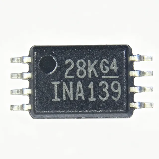
INA240A1QPWRQ1 - 20V/V Current Sense Amp AEC-Q100 | Texas Instruments
The Texas Instruments INA240A1QPWRQ1 is an AEC-Q100 qualified, voltage-output current sense amplifier with a fixed gain of 20 V/V (A1 version), delivered in an 8-pin TSSOP (PW) package rated from -40C to +125C. It senses voltage drops across shunt resistors over an exceptionally wide common-mode voltage range of -4V to 80V, independent of the 2.7V to 5.5V supply voltage. A current sense amplifier is a specialized difference amplifier optimized to accurately measure small shunt voltages riding on high common-mode potentials. Within the power-management IC hierarchy, it sits between the shunt resistor and an ADC or controller, converting current into a ground-referenced analog voltage. Current sensing is fundamental to motor control, battery management, and overcurrent protection in automotive and industrial systems. Key features include ultra-precise zero-drift architecture with very low offset and drift, a bidirectional output configurable via REF1 and REF2 pins, and enhanced PWM rejection. The enhanced PWM rejection is the defining differentiator: it suppresses large common-mode transients common in PWM-driven inverter stages, where conventional current sense amplifiers saturate and corrupt the measurement for several microseconds after each switching edge. The device provides reference pins to configure operation as either unidirectional or bidirectional output swing. The negative common-mode capability down to -4V allows operation below ground, accommodating the flyback period of typical solenoid and motor drive applications. The zero-drift topology delivers DC accuracy suitable for precision torque control and coulomb counting without periodic calibration. Typical applications include in-line motor phase current sensing in HEV/EV traction inverters, solenoid current monitoring, battery current monitoring in 12V and 48V systems, and DC bus current sensing in servo drives and solar inverters. Design tip: keep shunt resistor power dissipation in check by choosing the lowest gain version (20 V/V for the A1) that meets your ADC input range, and place the INA240 close to the shunt with tight, symmetric Kelvin routing to INP and INN to preserve the enhanced PWM rejection performance.

IRS2093MTRPBF - 4-Ch Class D Audio Driver, 100V, 0.6A | Infineon
The Infineon IRS2093MTRPBF is a 4-channel protected Class D audio amplifier driver integrating high-voltage gate drivers with PWM modulators in a 48-pin MLPQ (PG-VQFN-48) package. Per the manufacturer datasheet, it delivers 0.6 A gate-drive current at up to 100 V bus voltage, supports half-bridge and full-bridge topologies, and includes programmable over-current protection plus programmable dead-time generation. The device is supplied on Tape & Reel (TR) and is a lead-free, RoHS-compliant part designed for home audio and professional amplifier systems. A Class D audio amplifier is a switching amplifier topology that uses pulse-width modulation (PWM) to drive a power stage at high efficiency (typically 85-95%) rather than dissipating energy as heat like a linear (Class A/B) amplifier. The IRS2093MTRPBF sits in the controller/driver tier of the Class D hierarchy - it contains the modulator and gate drivers but requires external power MOSFETs and an output LC filter. This makes it part of the broader audio amplifier IC family within power management and amplifier IC categories. Key features include four independent floating analog inputs with PWM modulators, integrated high-side/low-side gate drivers capable of 0.6 A sink/source, programmable dead-time to prevent shoot-through, programmable over-current protection (OCP) with auto-recovery, under-voltage lockout (UVLO) for both VCC and VBS rails, and a protection control interface pin (SD/OTW) for fault reporting and thermal warning. The 48-pin MLPQ package provides an exposed thermal pad to dissipate gate-driver losses. Architecture-wise, the IRS2093MTRPBF uses a bipolar CMOS-DMOS (BCD) high-voltage process that allows the floating high-side driver to operate up to 100 V while the low-side and logic sections operate from lower rails. Each channel's modulator accepts a small-signal analog input and generates complementary PWM outputs at the gate driver stage, with dead-time inserted between the high-side and low-side switches to prevent cross-conduction. Typical applications include 4-channel home theater amplifiers, 2.1/4.1 subwoofer-and-satellite systems, multi-channel professional audio amplifiers, automotive head-unit amplifier stages, and powered studio monitor speakers. The wide 100 V bus rating supports high-power designs (several hundred watts per channel into 4 ohms) when paired with appropriately rated external MOSFETs. Design consideration: the IRS2093MTRPBF requires a carefully designed output LC reconstruction filter per channel - component values depend on switching frequency (typically 350-500 kHz), load impedance, and desired audio bandwidth. Incorrect filter design is the most common source of EMI, THD degradation, or instability in Class D designs using this driver. This page synthesizes distributor pricing, drop-in alternatives, and practical design considerations not found in the manufacturer datasheet alone, giving engineers a faster path from selection to working prototype.

LM2902KNSE4 - Quad 26V 1.2MHz Op-Amp | Texas Instruments
The Texas Instruments LM2902KNSE4 is a quad general-purpose operational amplifier with four independent high-gain, internally frequency-compensated amplifier circuits in a 14-pin SOIC (5.30 mm width) surface-mount package. Each amplifier offers a 1.2 MHz gain-bandwidth product, a 0.5 V/us slew rate, and operation from a single supply up to 26 V (or dual supplies of +/-13 V), with a typical supply-current drain of 0.8 mA that is largely independent of supply voltage. A quad operational amplifier is an analog IC that integrates four op-amp cores on a single die, sharing supply and ground pins while keeping each amplifier's inputs and outputs independent. Op-amps belong to the linear-amplifier family of semiconductors, positioned under the broader categories of amplifiers, analog signal conditioning ICs, and power management signal chains. Quad integration reduces board area, bill-of-material count, and per-channel cost compared with four single op-amps. Key features of the LM2902KNSE4 include a wide single-supply range (3 V to 26 V), common-mode input range that extends to ground (ground-sensing capability), and the automotive temperature grade associated with the LM2902 family. The improved LM2902K variant adds a 2 kV ESD rating per TI product information. Outputs can source and sink current without external protection in most configurations, and the internal compensation removes the need for external frequency-setting components. Architecturally, the LM2902 follows the classic bipolar silicon process used in industry-standard quad op-amps. The internal 1.2 MHz compensation makes each channel unity-gain stable, while the low, supply-independent quiescent drain supports battery-powered and low-power industrial designs. The biasing scheme keeps channel-to-channel coupling low, so one amplifier driving a load does not materially disturb the others. Typical applications include automotive signal conditioning (sensor buffers and comparators on 12 V/24 V rails), industrial control loops and 4-20 mA transmitters, active filters and summing stages in audio and instrumentation, and low-side current-sense amplification in power supplies. The automotive grade and wide supply range make it well suited to vehicle-level electronics where cold-crank and load-dump conditions compress supply headroom. When designing with this device, keep the common-mode input range within the datasheet limits - inputs beyond the negative rail can cause phase inversion, and outputs cannot swing fully to the positive rail under load. Decouple the shared supply pin with 0.1 uF placed close to pin 4. This page adds value beyond the manufacturer datasheet: distributor sourcing links, drop-in alternative comparisons with parametric matching, per-application design guidance, and layout notes compiled from TI application literature.

LM2903AQS-13 - Dual 36V AEC-Q100 Comparator | Diodes Inc
The Diodes Incorporated LM2903AQS-13 is an automotive-grade dual differential voltage comparator with a wide supply range of 2V to 36V on a single supply (or ±1V to ±18V on dual supplies), a typical input offset voltage of 1mV, and open-collector outputs in an 8-pin SOIC (SO-8) package qualified to AEC-Q100. A voltage comparator is an analog building block that compares two input voltages and drives its output to indicate which is higher. Within the power-management and signal-conditioning hierarchy, comparators sit alongside operational amplifiers and voltage references; unlike an op-amp, a comparator is intentionally uncompensated for fastest switching and is used with an open-collector output stage to interface directly with TTL and CMOS logic. Key features of the LM2903AQS-13 include very low input offset voltage (1mV typical), low input bias current of 25nA, and low supply current drain of approximately 0.6mA per comparator, which makes the device suitable for battery-powered designs. The common-mode input voltage range includes ground even when operated from a single supply, allowing the part to sense signals near 0V without an external negative rail. The device belongs to the industry-standard LM2901Q/LM2903Q family from Diodes Incorporated. Outputs are open-collector, so pull-up resistors are required and multiple outputs can be wired-OR for window-comparator or over-voltage/under-voltage detection topologies. Rail-to-rail output swing to the positive rail is achieved through the external pull-up, and the output stage sinks current to ground with saturation voltage low enough to drive TTL logic directly. Typical applications include automotive sensor monitoring and limit detection, over-voltage and under-voltage supervisors, window comparators on industrial 24V-rail systems, oscillator and Schmitt-trigger circuits, and battery-management threshold detection in portable equipment. The automotive qualification (AEC-Q100) makes it especially appropriate for in-vehicle modules exposed to -40C to +125C ambient conditions. When designing with this part, remember that the open-collector output requires a pull-up resistor; the pull-up may be referenced to any voltage up to the 36V absolute maximum regardless of the comparator supply. Input common-mode range must be respected at the negative extreme, and hysteresis (a few millivolts via positive feedback) should be added when comparing slowly moving signals to prevent output chatter. This page synthesizes distributor inventory listings, drop-in cross-reference data, and practical design notes not found in the manufacturer datasheet, providing a single quotable reference for sourcing and design engineers.
LM2903EDR2G - Dual 36V Low Offset Comparator | onsemi | SOIC-8
The onsemi LM2903EDR2G is a dual independent precision voltage comparator with a maximum supply rating of 36 V (±18 V split supply), a low input offset voltage of 2.0 mV, and an open-collector output stage, housed in an 8-pin SOIC (SO-8) surface-mount package supplied in tape and reel packing (R2 suffix). A voltage comparator is an analog building block that compares two input voltages and drives its output to indicate which input is higher. Comparators sit within the broader amplifier IC family - related to operational amplifiers but optimized for fast, saturated switching rather than linear amplification - and are fundamental elements of power management, signal conditioning, and mixed-signal systems. Dual comparators such as the LM2903 family integrate two independent comparator cells in one package, halving board area versus two single-channel parts. Key features of the LM2903EDR2G include single-supply operation from roughly 2 V up to 36 V, a common-mode input range that extends down to ground level (negative rail), and an open-collector output that allows wire-OR connection of multiple comparators and simple interfacing to logic levels up to the supply rail through an external pull-up resistor. The low 2.0 mV input offset voltage specification permits accurate threshold detection with modest hysteresis network design. Technically, the device uses a differential PNP input stage, which is what allows the input common-mode range to reach ground even when powered from a single positive supply. The output transistor sinks current to ground while the pull-up resistor defines the logic-high level, making the part level-flexible across 5 V, 12 V, 24 V, and 36 V industrial rails. Typical applications include overvoltage and undervoltage monitoring, limit comparators in power supplies, window detectors, square-wave and relaxation oscillators, and analog-to-digital threshold interfacing in industrial automation equipment. A key design consideration: because the open-collector output only sinks current, every output requires a pull-up resistor, and response time depends strongly on the chosen pull-up value - lighter pull-ups trade speed for lower power. This page synthesizes distributor availability data, pin-compatible drop-in alternatives, and practical design notes in one place - information not consolidated in the manufacturer datasheet alone.

LM2903FVM-TR - Dual Ground-Sense Comparator | ROHM Semiconductor
The ROHM Semiconductor LM2903FVM-TR is a dual ground-sense comparator with an operating voltage range of 3 V to 32 V, supplied in an 8-MSOP package. It combines two comparator channels, a common-mode input range intended for ground-sense applications, and low supply-current operation for use across industrial, automotive, and embedded control systems. The -TR ordering code identifies the tape-and-reel shipping configuration. A ground-sense comparator is a voltage comparator optimized for detecting signals near the lower end of its supply range. Within the broader semiconductor hierarchy, it belongs to the analog IC, comparator, and signal-conditioning categories. Its two channels can monitor separate low-voltage nodes, compare input thresholds, and produce logic-compatible decisions for control systems where sensing close to ground improves measurement resolution. ROHM describes the LM2903FVM as a two-channel ground-sense comparator with a wide 3 V to 32 V operating range and low supply current. Distributor technical summaries identify the device as a dual, general-purpose, open-collector comparator in an 8-pin MSOP package. The dual-channel configuration reduces component count when two independent ground-related thresholds must be evaluated in the same circuit. The open-collector output architecture allows the output node to be pulled up to an external supply, making the interface suitable for wired logic levels, system-level fault signaling, and retrofit designs based on open-collector comparators. Because the output transistor is not driven actively high, external pull-up resistors determine the high output voltage and must be selected for the target interface. The output transistor also provides a practical way to combine comparator indications when wired logic functions are required. Typical uses include monitoring low-voltage power rails, detecting undervoltage conditions, checking sensor returns near ground, and implementing threshold-based protection in industrial or automotive equipment. Because the device supports operation up to 32 V according to the manufacturer product page, it is useful in systems whose supply voltage exceeds the range of many low-voltage comparator ICs. The -40 °C to 125 °C temperature range supports operation across extended industrial temperature environments. Design the input network so the sensed voltages remain within the comparator's specified common-mode limits, and account for input offset and propagation delay when setting a threshold. Select the pull-up resistor using the required output rise time, load capacitance, and allowable sink current. Place the device and its bypass capacitor near the protected circuit, and route sensitive input traces away from switching nodes to reduce false threshold transitions. This product page combines manufacturer information, package details, sourcing guidance, application analysis, and pin-compatible replacement screening. It also distinguishes true same-footprint drop-in choices from devices that merely perform a similar comparison function, helping engineers evaluate PCB reuse without making changes that could compromise signal behavior or application conditions.
LM2904D - Dual 26V 700kHz Op Amp | Texas Instruments (Tape & Reel)
The LM2904D from Texas Instruments is a dual operational amplifier designed for general-purpose analog applications requiring low power and a wide supply range. It operates from a single supply of 3V to 26V or dual supplies of ±1.5V to ±13V, with a typical supply current of 500uA per amplifier, in an 8-pin SOIC (D) package rated for -40C to +125C. An operational amplifier (op amp) is a high-gain voltage amplifier with differential inputs and a single-ended output. It is a fundamental building block of analog electronics within the hierarchy: op amp -> amplifier IC -> linear IC -> semiconductor. General-purpose dual op amps like the LM2904 integrate two independent amplifiers in one package, reducing board space and component count compared to two single op amps. Key features include a gain bandwidth product of 700 kHz, a slew rate of 0.3 V/us, and an input offset voltage of 2 mV (typical). The common-mode input voltage range includes ground, enabling direct ground-sensing in single-supply systems. The output swings close to the negative rail, and internal short-circuit protection plus a latch-up-free input stage make the device robust in automotive and industrial environments. The LM2904 uses bipolar transistor architecture with a class AB output stage, providing low output impedance and reasonable drive capability. Internal frequency compensation guarantees unity-gain stability without external components, and supply current is essentially independent of supply voltage. Quiescent drain of 0.7 mA (typical) suits battery-powered designs. Typical applications include transducer amplifiers, DC gain blocks, active filters, voltage followers, and signal conditioning front-ends in automotive ECUs, industrial sensors, and consumer electronics. According to the TI LM2904 datasheet, no latch-up occurs when the common-mode range is exceeded, an advantage in voltage-follower circuits. Design tip: decouple VCC with a 0.1uF ceramic capacitor placed close to pin 8, keep inputs within the specified common-mode range for best accuracy, and note the output can drive loads down to about 2 kohm; use a buffer stage for heavier loads. Pricing references are as of 2026-08-30.
LM2904DR - Dual 26V 700kHz Op Amp | Texas Instruments
The LM2904DR from Texas Instruments is a dual operational amplifier designed for general-purpose analog applications requiring low power and a wide supply range. It operates from a single supply of 3V to 26V or dual supplies of ±1.5V to ±13V, with a typical supply current of 500uA per amplifier, in an 8-pin SOIC (D) package rated for -40C to +125C. An operational amplifier (op amp) is a high-gain voltage amplifier with differential inputs and a single-ended output. It is a fundamental building block of analog electronics within the hierarchy: op amp -> amplifier IC -> linear IC -> semiconductor. General-purpose dual op amps like the LM2904 integrate two independent amplifiers in one package, reducing board space and component count compared to two single op amps. Key features include a gain bandwidth product of 700 kHz, a slew rate of 0.3 V/us, and an input offset voltage of 2 mV (typical). The common-mode input voltage range includes ground, enabling direct ground-sensing in single-supply systems. The output swings close to the negative rail, and internal short-circuit protection plus a latch-up-free input stage make the device robust in automotive and industrial environments. The LM2904 uses bipolar transistor architecture with a class AB output stage, providing low output impedance and reasonable drive capability. Internal frequency compensation guarantees unity-gain stability without external components, and supply current is essentially independent of supply voltage. Quiescent drain of 0.7 mA (typical) suits battery-powered designs. Typical applications include transducer amplifiers, DC gain blocks, active filters, voltage followers, and signal conditioning front-ends in automotive ECUs, industrial sensors, and consumer electronics. According to the TI LM2904 datasheet, no latch-up occurs when the common-mode range is exceeded, an advantage in voltage-follower circuits. Design tip: decouple VCC with a 0.1uF ceramic capacitor placed close to pin 8, keep inputs within the specified common-mode range for best accuracy, and note the output can drive loads down to about 2 kohm; use a buffer stage for heavier loads. Pricing references are as of 2026-08-30.

LM393 - Dual Open-Collector Comparator | Texas Instruments
The Texas Instruments LM393 is a dual independent precision voltage comparator designed for single or split-supply operation, with a 2 V to 30 V supply range, common-mode input operation extending to ground, and open-collector outputs in an 8-pin SOIC surface-mount package. The two comparators operate independently and require no external output pull-up when their outputs are used as open-drain signals. A voltage comparator is an analog semiconductor that compares two input voltages and produces a digital output indicating their relative relationship. The LM393 belongs to the comparator hierarchy within analog ICs and broader signal-conditioning and power-management systems. Unlike an operational amplifier, its output is intended to switch actively and can operate from a single supply while accepting an input common-mode range down to ground. Key features include two independent comparator channels, differential input voltage capability up to ±38 V, and compatibility with TTL, MOS, and CMOS logic. The open-collector output allows a designer to set the output logic voltage through an external pull-up resistor. This architecture is useful when driving multiple wired-open outputs, connecting to a bus, or interfacing with a supply domain different from the comparator output pull-up. The LM393 can operate from a single supply or split supply, while the common-mode input range reaches ground for many sensing conditions. Its differential input limit equals the maximum-rated supply voltage, but the absolute maximum rating should not be interpreted as a normal operating range. Input protection, supply sequencing, and output pull-up selection remain important design constraints. Typical uses include window detection in power supplies, battery monitoring, sensor threshold conditioning, industrial control interfaces, automotive electronics, and consumer equipment. In each case, the LM393 provides a simple high-or-low decision without the output stage normally associated with a push-pull logic device. For reliable designs, select the correct package ordering code, verify the temperature grade, place decoupling close to the supply pins, and use a pull-up resistor sized for the intended logic family and output-current limit. Check input transients against the absolute maximum ratings rather than relying on nominal common-mode limits. This page combines the LM393 device description with functional guidance, drop-in replacement considerations, application patterns, and engineering-oriented comparisons. It helps buyers distinguish the open-collector dual comparator from op-amp alternatives while supporting package, temperature, and lifecycle decisions before requesting a quote.
LM393AMX - Dual Differential Comparator 36V SOIC-8 | onsemi
The onsemi LM393AMX is a dual differential voltage comparator with supply operation from 2V to 36V single-supply (±1V to ±18V dual-supply), a typical supply current of 800 uA, packaged in an 8-pin SOIC (SOIC-8, 3.90mm body width) delivered in Tape and Reel packaging. A voltage comparator is an analog integrated circuit that compares two input voltages and drives its output to indicate which input is higher. Comparators form the sensing layer of the signal-chain hierarchy: they sit between sensors or dividers and digital logic, translating analog thresholds into logic-level decisions. The LM393 family, originally introduced by Fairchild Semiconductor and now manufactured by onsemi, remains the industry-standard general-purpose dual comparator. Key features include comparison of voltages near ground potential thanks to an input common-mode range that extends to the negative rail, open-collector outputs compatible with all forms of logic (TTL, CMOS, RTL, DTL, MOS), and low current drain of 800 uA typ that suits battery-powered designs. The dual-channel integration lets one comparator monitor a threshold while the second implements hysteresis or a second independent trip point. Architecturally, the LM393AMX uses a PNP differential input stage that allows common-mode input voltages down to ground on a single supply. The uncommitted open-collector output stage requires an external pull-up resistor, which lets the designer set the output logic level to 5V, 3.3V, or any rail up to the supply maximum, simplifying interfacing with mixed-logic systems. The part is specified across the industrial temperature range, and the A-suffix denotes an enhanced-specification grade over the base LM393. Typical applications include threshold detection and limit monitors, zero-crossing detectors in power conversion, oscillator and relaxation-clock generation, level shifting between logic families, sensor interfacing with photodiodes or thermistors, and over-voltage/under-voltage supervision on 24V industrial buses. When designing with this device, remember that open-collector outputs need a pull-up resistor and that small hysteresis (a few millivolts via positive feedback) prevents output chatter on slowly moving inputs near the threshold. This page synthesizes distributor sourcing information, verified drop-in alternatives with package and parameter matching, and practical design notes not found in the manufacturer datasheet.

LT6350IDD#PBF - Low Noise SE-to-Diff ADC Driver | ADI
The Analog Devices LT6350IDD#PBF is a rail-to-rail input and rail-to-rail output low-noise single-ended-to-differential converter and ADC driver housed in an 8-lead DFN (3 mm x 3 mm) exposed-pad package. It accepts a high- or low-impedance single-ended input and produces a low-impedance, balanced differential output suitable for driving high-performance successive-approximation-register (SAR) ADCs. The two-op-amp internal topology is optimized for fast settling and low distortion at high ADC sampling rates. An ADC driver (also called a differential amplifier or SE-to-diff converter) is a specialized analog interface stage placed between a single-ended signal source and a differential-input ADC. Its job is to level-shift, gain-set, and convert the signal while preserving SNR and adding minimal noise and distortion. The LT6350 sits in the signal chain hierarchy of transducer -> front-end amplifier -> ADC driver -> SAR/Delta-Sigma ADC, where it is responsible for common-mode level shifting and differential gain setting. Key features include rail-to-rail input and output swing, very low input-referred voltage noise, fast settling for multi-MHz ADC sampling, integrated precision resistors, and a shutdown/ground-reference pin for power saving. The exposed-pad DFN package provides a low thermal-resistance path (~43 C/W typical) suitable for continuous operation at moderate quiescent current, and the differential output maintains balance across the ADC input common-mode range. The architecture uses two internally trimmed op amps with matched thin-film resistors that set the inverting and non-inverting gain paths. This topology achieves better than -94 dBc SFDR at 1 MHz and noise performance far superior to discrete op-amp + resistor implementations, eliminating the need for manual resistor matching. The internal reference and gain-setting resistors are laser-trimmed at the factory for accurate gain (typically gain = 2) and tight common-mode rejection. Typical applications include driving 16-/18-bit SAR ADCs in data-acquisition systems, medical imaging front ends, precision instrumentation, differential line drivers, and any signal chain where a single-ended source must be converted to a clean differential ADC input. The wide input common-mode range makes it well-suited to single-supply 5 V or 12 V systems, and the rail-to-rail outputs allow direct connection to modern low-voltage SAR converters. When designing with the LT6350, choose the gain setting via external resistor ratios (the internal resistors set the unity-noise-gain baseline), keep the exposed pad soldered to a sufficient copper pour for thermal relief, and decouple the supply with a 0.1 uF capacitor placed as close as possible to the V+ and V- pins. The shutdown pin should be tied to V+ if unused to minimize quiescent current draw. This page synthesizes distributor pricing, drop-in alternative listings, and applied design notes not found on the manufacturer datasheet alone, giving engineers a single reference for cross-brand equivalents, pinout, and thermal considerations for the LT6350IDD#PBF.

OPA4170-Q1 - Quad 36V 1.2MHz Low-Power Op Amp | TI Automotive
The Texas Instruments OPA4170AQPWRQ1 is a quad-channel, 36-V, single-supply, low-noise operational amplifier designed for automotive applications. It operates from 2.7 V (±1.35 V) to 36 V (±18 V) with a gain-bandwidth product of 1.2 MHz and a low quiescent current of 475 uA per channel, and comes in a 14-pin TSSOP (PW) package with AEC-Q100 qualification. An operational amplifier (op amp) is a high-gain voltage amplifier with differential inputs and a single-ended output, and is a fundamental building block of analog electronics used in signal conditioning, filtering, and amplification. Op amps sit within the hierarchy of linear integrated circuits, alongside comparators, voltage regulators, and references. The OPA4170-Q1 belongs to the value-line precision op amp family, offering low offset voltage and drift for accurate signal processing, and complements the single OPA170-Q1 and dual OPA2170-Q1 family members, which share identical per-channel specifications for maximum design flexibility. Key features include a low input offset voltage of 500 uV (max), low input bias current of 15 pA (max), and high common-mode rejection ratio (CMRR) of 120 dB. The wide supply range suits automotive battery-powered systems connected directly to 12-V and 24-V rails, while rail-to-rail input/output (RRIRO) maximizes dynamic range in single-supply designs - critical for sensor interfaces and motor control loops. Technically, the OPA4170-Q1 uses a CMOS input stage contributing to picoampere bias current and high input impedance. The rail-to-rail output stage swings close to the supply rails, and the device is stable with capacitive loads up to 300 pF, simplifying buffer designs. Internal ESD protection enhances robustness in harsh automotive environments. Typical applications include automotive battery management systems, motor control current sensing, and sensor signal conditioning, where its low power suits always-on modules. Design tip: decouple supply pins with 0.1 uF ceramic capacitors placed close to the device, and verify the input common-mode range in single-supply designs.
OPA858IDSGR - 5.5GHz GBWP FET-Input TIA Amplifier | Texas Instruments
The Texas Instruments OPA858IDSGR is a decompensated, wideband operational amplifier with CMOS (FET) inputs, optimized for transimpedance amplifier (TIA) and wideband voltage amplifier applications. It delivers a 5.5 GHz gain bandwidth product (GBWP) in a compact 8-pin WSON (DSG) package measuring 2x2 mm, operating from a 3.3V to 5.25V supply across the -40C to +125C industrial temperature range. A transimpedance amplifier is an operational amplifier topology that converts a current input, typically from a photodiode, into a proportional voltage output. Within the amplifier hierarchy, the OPA858 belongs to the high-speed, FET-input operational amplifier family, part of the broader class of analog signal conditioning ICs. Its 5.5 GHz GBWP enables high closed-loop bandwidths at transimpedance gains in the range of tens to hundreds of kilohms, making it ideal for optical front-end receiver chains. Key features include a low input voltage noise of 2.5 nV/sqrt(Hz), extremely low input bias current from the FET input stage, and a high slew rate for fast settling on pulsed signals. The decompensated architecture delivers higher bandwidth at closed-loop gains of 7 V/V or greater compared to unity-gain-stable amplifiers, but requires careful feedback network design to guarantee stability. The CMOS input stage provides extremely high input impedance, essential for accurate current-to-voltage conversion in photodiode applications. The small WSON-8 package with exposed thermal pad minimizes parasitic inductance and aids heat dissipation, both critical at gigahertz-class bandwidths. Typical applications include LIDAR receivers, optical network receivers, high-speed data acquisition, and test and measurement equipment. The device also buffers high-speed DAC outputs and drives high-speed ADC input stages. When designing with the OPA858, select the feedback capacitor carefully to optimize the bandwidth-stability trade-off, minimize parasitic capacitance at the inverting input through tight PCB layout, and solder the exposed pad to a solid ground plane. Pricing reference: approximately $3.15 at LCSC as of 2026-08-30.