DC-DC Converters
بەرهەمەکان (770+)

MIC23150-GYMT-TR - 4MHz 2A Sync Buck Regulator 1.8V | Microchip
The Microchip Technology MIC23150-GYMT-TR is a 4MHz 2A HyperLight Load synchronous buck (step-down) switching regulator with a fixed 1.8V output, 2.7V to 5.5V input range, and 23uA quiescent current, housed in an 8-pin 2x2 mm TDFN (thin MLF-8) package less than 1mm tall. A synchronous buck regulator is a type of DC-DC switching converter that steps a higher input voltage down to a lower output voltage using a high-side and a low-side (synchronous rectifier) MOSFET integrated on the die, replacing the external Schottky diode of a conventional buck converter to improve efficiency. Within the power management hierarchy - power management IC, switching regulator, buck converter - the MIC23150 targets battery-powered and space-constrained point-of-load applications. Key differentiating features include the proprietary HyperLight Load mode, which combines 4MHz PWM operation in continuous conduction with ultra-fast transient response and very high light-load efficiency; peak efficiency of 93% in continuous conduction mode; and support for a very small 0.47uH inductor with an output capacitor as small as 2.2uF, enabling a complete solution under 1mm height. The 4MHz switching frequency moves noise far above sensitive RF and audio bands and shrinks the magnetics to tiny chip inductors. Architecturally, the device integrates both power MOSFETs, the 4MHz oscillator, and the HyperLight Load control loop, which automatically transitions between PWM and ultra-light-load operation to keep output ripple very low across the entire load range. This makes it well suited to powering processor core rails that swing from sleep-level microamp loads to full 2A bursts with minimal droop. Typical applications include supplying processor and SoC core voltages, point-of-load rails in portable and battery-powered devices, RF module power supplies in cellular and IoT terminals, and embedded power management in space-limited industrial designs. The 2.7V-5.5V input range directly accepts single-cell Li-ion batteries and 5V rails. Design consideration: at 4MHz, layout discipline is critical - keep the input capacitor, inductor, and SW node loop as small as possible, and select a low-DCR 0.47uH inductor rated above 2A to preserve efficiency and transient performance. This page synthesizes distributor pricing, verified drop-in alternative data, and practical design guidance not found in the manufacturer datasheet alone.

MIC23201YML - 2A 2MHz Sync Buck Regulator w/ HSC | Microchip
The Microchip MIC23201YML is a high-efficiency 2 MHz synchronous buck (step-down) DC-DC regulator delivering up to 2 A of output current from a 2.7 V to 5.5 V input, housed in a 10-pin 3 mm × 3 mm MLF/VFQFN exposed-pad package. It features Hyper Speed Control (HSC) architecture that delivers ultra-fast transient response suited for processor core voltages and other dynamic loads, plus an adjustable output from 0.95 V to 3.6 V via an external resistor divider. A synchronous buck regulator (also called a step-down switching regulator) is a type of DC-DC converter that uses PWM-controlled MOSFET switches and an LC output filter to produce a lower output voltage than its input with very high efficiency - typically 90-95% versus 30-60% for a linear (LDO) regulator. Synchronous designs replace the conventional Schottky rectifier with a low-side MOSFET to further reduce conduction losses. Within the broader power-management hierarchy, buck regulators sit between simple LDOs and more complex multi-phase controllers; they are the workhorse of point-of-load (POL) conversion in nearly every portable, embedded, and SoC-based system. The MIC23201YML differentiates itself through its Hyper Speed Control loop, which adapts the switching behavior cycle-by-cycle rather than relying on a fixed-frequency PWM modulator. This produces a transient response that recovers from a load step in microseconds - critical when powering ASICs, FPGAs, and SoCs whose core voltages may demand hundreds of milliamps of step current in nanoseconds. Internal MOSFETs (typical 65 mΩ high-side / 65 mΩ low-side) minimize the need for external switches, and the part requires only a small inductor, a few ceramic capacitors, and feedback resistors to form a complete 2 A supply. Key specifications include a 2.7 V to 5.5 V input range, 0.95 V to 3.6 V adjustable output, 2 A continuous output current, 2 MHz typical switching frequency, internal soft-start, thermal-shutdown and current-limit protection, and a junction operating temperature up to +125 °C. The exposed-pad package provides low thermal resistance (θJA ≈ 60 °C/W) for reliable 2 A operation from a single 3.3 V or 5 V rail. Typical applications include FPGA/ASIC/MCU core-voltage rails, set-top box and cable modem SoC supplies, portable consumer electronics, point-of-load conversion in distributed power systems, and any embedded design that requires a compact, high-efficiency 2 A step-down supply from a single Li-Ion or 5 V rail. When designing with this device, select a 1 µH to 4.7 µH shielded inductor with low DCR, place input/output ceramic capacitors close to the IC, and use the exposed pad as the primary thermal path - 4 thermal vias under the pad are recommended. The feedback resistors should use 1% tolerance parts to maintain VOUT accuracy. This page synthesizes distributor pricing, drop-in alternatives, and practical design notes not found in the manufacturer datasheet.
MIC23303YML-T5 - 3A 4MHz HyperLight Load Sync Buck | Microchip
The Microchip Technology MIC23303YML-T5 is a high-efficiency 4MHz 3A synchronous step-down buck regulator with HyperLight Load mode, Power Good output indicator, and programmable soft-start, housed in a 12-pin 3mm x 3mm VDFN exposed-pad package. It delivers up to 3A of output current from a 2.7V to 5.5V input rail, with an adjustable output from 0.65V up to 3.6V, making it a compact point-of-load solution for low-voltage digital cores. A buck regulator (also called a step-down switching converter) is a power management IC that efficiently converts a higher DC input voltage to a lower DC output voltage using high-frequency switching of an internal MOSFET pair, an external inductor, and an output capacitor. Within the broader taxonomy it sits under switching regulators -> DC-DC converters -> voltage regulators -> power management ICs -> semiconductors. Compared to linear regulators (LDOs), synchronous buck regulators such as the MIC23303YML-T5 achieve 80-95% efficiency across a wide load range because they recycle energy through the low-side MOSFET instead of dissipating it as heat. Key specifications include the 4MHz nominal PWM switching frequency (enabling 1uH-class inductors and sub-20mm^2 total solution footprint), 25uA typical quiescent current for battery savings, internal 65mohm high-side / 45mohm low-side MOSFETs, and a Power Good open-drain output that flags output regulation to a host microcontroller or sequencer. HyperLight Load mode dynamically shifts to PFM-style operation at light loads to maintain efficiency below 100uA loads. Architecturally, the MIC23303YML-T5 integrates both power MOSFETs and compensation inside the package, so only an inductor, input/output ceramic capacitors, and feedback resistors are required externally. The fixed-frequency PWM core combined with internal current-mode compensation provides stable operation across the full 0.65V-3.6V output range and across the -40C to +125C junction temperature window. Typical applications include powering 1.0V/1.2V/1.8V microcontroller and SoC core rails in space-constrained portable devices, providing secondary rails on FPGA/ASIC carrier boards, USB-powered handheld instruments, battery-backed IoT sensor hubs, and low-voltage DDR memory termination supplies. The 3A capability and 0.65V minimum output cover the bulk of sub-3.3V digital load points. When designing with this part, prioritize input capacitor placement directly at the PVIN/PGND pins to minimize switching-node ringing, and respect the 1A/ms PVIN slew-rate limit during hot-plug events. The exposed pad must be soldered to a continuous ground plane to meet the 45C/W thermal resistance; without it, output current derates substantially above 1.5A. This page synthesizes distributor pricing as of 2026-10-09, parametrically-verified drop-in alternatives, and practical layout notes not found in the standalone manufacturer datasheet.

MIC28516T-E/PHA - 70V/8A Sync Buck Regulator | Microchip
The Microchip Technology MIC28516T-E/PHA is a 70V-input, 8A-output synchronous DC/DC buck regulator featuring Hyper Speed Control adaptive on-time architecture, integrated low-FOM N-Channel trench FETs, and external soft start in a 32-pin VQFN-EP (5x5 mm) package. It operates from 4.5V to 70V input with adjustable output from 0.6V to 32V and ±1% output accuracy. A buck regulator (step-down switching converter) is a power management IC that efficiently converts a higher DC input voltage to a lower DC output voltage using high-speed switching of integrated power MOSFETs and energy storage in an external inductor and capacitor. Within the broader power management hierarchy, buck regulators sit under DC-DC converters, which themselves belong to the power management IC (PMIC) family. The synchronous topology replaces the traditional Schottky rectifier with a low-side FET, dramatically improving efficiency at high output currents. Key specifications include 8A continuous output current, 4.5V-70V wide input range, 0.6V-32V adjustable output, and Hyper Speed Control that delivers ultra-fast transient response without the loop-compensation complexity of classical voltage-mode controllers. Additional features include external soft-start, internal high-side bootstrap switch, thermal-shutdown, input undervoltage lockout, and a PGOOD indicator. The 32-VQFN exposed-pad package provides a low thermal-resistance path for dissipating power at full 8A load. Internally, the MIC28516 uses Microchip's enhanced adaptive on-time Constant On-Time (COT) controller co-packaged with a pair of low figure-of-merit N-Channel trench MOSFETs. This architecture eliminates the need for external compensation components and achieves fast transient response by modulating the on-time based on input voltage, output voltage, and desired switching frequency - typically 200 kHz to 1 MHz adjustable. Typical applications include industrial 24V/48V point-of-load regulation, telecom and networking equipment power, automotive 12V/24V accessory rails, battery-powered systems up to 60V, distributed power architectures, and general-purpose wide-Vin step-down conversion. Designers value this part when they need a high-current, wide-Vin buck in a compact thermally-enhanced package without writing a compensation network. When designing, choose the external feedback resistor divider for the desired output, size the inductor for 20-40% peak-to-peak ripple, and use ceramic output capacitors with low ESR. The exposed pad must be soldered to a sufficient copper pour (typically 1 sq inch minimum) to keep junction temperature within the 125C operating limit at full 8A load. This page synthesizes distributor pricing, parametric drop-in alternatives, and practical PCB layout/design notes not found in the manufacturer datasheet alone.

MIE1W0505BGY - 1W Isolated DC/DC Module, 5V Out | MPS
The Monolithic Power Systems MIE1W0505BGY is an isolated, regulated DC/DC power module delivering up to 1W of output power (5V output at 200mA) from a 3V to 5.5V input range, housed in a compact SOIC-16 wide body (WB) surface-mount package. An isolated DC/DC converter is a power module that transfers energy across a galvanic isolation barrier, keeping the secondary-side ground independent of the primary-side ground. Isolated converters sit within the power management IC hierarchy: power module -> isolated DC/DC converter -> switching regulator -> power supply. They are essential wherever ground loops, different voltage domains, or safety isolation are required, such as isolated communication interfaces, industrial sensor nodes, and gate-drive bias supplies. The MIE1W0505BGY stands out for its use of capacitive isolation technology for the feedback (FB) path, which regulates the output voltage without a traditional optocoupler or a precision-configurable reference IC. Eliminating the optocoupler reduces component count, improves long-term reliability (optocoupler CTR degrades over time), and enables a much smaller solution size than conventional 1W isolated modules. The module provides excellent load and line regulation across its full 3V-5.5V input range. Architecturally, the module integrates the power transformer, controller, synchronous rectification, and the capacitive FB isolator inside the SOIC-16WB molded body, presenting a single component that replaces a multi-component flyback design. Continuous short-circuit protection (SCP) and over-temperature protection (OTP), cited for the -5R-AEC1 family variant, safeguard the module against output faults and thermal stress. Typical applications include isolated RS-485/CAN transceiver bias supplies, isolated side-rails for gate drivers, industrial PLC I/O channel isolation, and 3.3V/5V logic-domain isolation in test equipment and battery-powered instruments. Design-wise, the wide 3V-5.5V input range lets a single module serve both 3.3V and 5V logic rails; verify that available input current margin covers the roughly 300mA-plus primary-side demand at 3.3V input for a full 200mA load. This page synthesizes distributor sourcing data, drop-in family alternatives, and practical design notes not found in the manufacturer product page.

MP1251DS-LF - Specialized Power-Supply Interface | MPS
The Monolithic Power Systems MP1251DS-LF is a specialized power-supply and converter interface integrated circuit packaged in an 8-pin SOIC. The verified distributor data identifies the device as a Last Time Buy part and lists an SMBus interface, SMT mounting, and suitability for power supplies, converters, and controller-interface applications. Those verified facts define its present role, while detailed electrical limits, timing values, register functions, and pin-level functions were not supplied and must be confirmed from the manufacturer datasheet before design release. A power-supply interface controller is a specialized class of power-management and interface IC that sits between a host controller and a regulated power subsystem. An SMBus-compatible device may be used for configuration, telemetry, control, or status exchange, but the exact commands and electrical implementation of MP1251DS-LF cannot be inferred from the distributor category alone. System designers should therefore treat the verified part identity, package, interface category, applications, mounting style, and lifecycle state as authoritative while sourcing missing functional data from the original documentation. The 8-SOIC package supports surface-mount PCB assembly and matches the package information reported by DigiKey and GlobalSpec. Surface mount is useful in compact power electronics because it avoids through-hole mechanical strain and supports automated assembly. However, the verified material does not provide body dimensions, pin pitch, thermal resistance, maximum supply voltage, operating temperature, current rating, or exposed-pad details. Those package and electrical attributes should not be inferred from the generic 8-SOIC label. Typical design targets suggested by the verified distributor records are power supplies, DC-DC converters, and controller-interface systems. In each case, the device should be evaluated for protocol compatibility, signal levels, timing, operating voltage, shutdown behavior, and fault handling. Because MP1251DS-LF is identified as Last Time Buy, procurement planning matters as much as electrical suitability. Buyers should confirm current distributor inventory, lifecycle timing, and authorized-channel traceability before committing a new production design. The most important layout precaution is to follow the exact manufacturer pinout and recommended decoupling once the original datasheet is obtained. Do not assign SOIC pins by convention or route SMBus signals before confirming their package numbers and alternate functions. Validate pull-ups, voltage-domain compatibility, ground return paths, and any exposed thermal or electrical requirements at the schematic-review stage. This product record consolidates the verified distributor status, package, interface class, application labels, source links, and sourcing implications for MP1251DS-LF. It deliberately leaves unavailable electrical and pin functions unresolved rather than manufacturing specifications, and it distinguishes verified purchasing information from engineering data that still requires manufacturer documentation.
MP1252DS-LF - Specialized 8-SOIC Power Interface | MPS
The Monolithic Power Systems MP1252DS-LF is a specialized power-supply, converter, and controller interface IC packaged in an 8-pin SOIC. The verified distributor data identifies the device as an 8-SOIC component, while its detailed electrical ratings, pin functions, operating limits, internal architecture, and application-specific performance are not included in the supplied records. Those unverified parameters are therefore reserved for datasheet review rather than inferred from the product category. A power-supply interface IC is a specialized block within the power-management semiconductor hierarchy. It can connect or control power-conversion functions, regulate system rails, or supervise power-system behavior depending on its internal implementation. Unlike a generic logic IC, such a device is selected for the electrical conditions and control functions associated with a power rail rather than for Boolean processing alone. The MP1252DS-LF belongs to this broader class of power-management ICs but should not be assigned a more specific regulator, converter, or controller function without confirmation from the manufacturer datasheet. The verified catalog record establishes an 8-SOIC package and categorizes the MP1252DS-LF as a specialized power-supplies, converters, and controllers interface part. Its package supports compact surface-mount assembly, but no verified dimensions, pin orientation, exposed pad, thermal rating, or land-pattern details are supplied. The distributor listings also associate the device with RoHS3 compliance, although the manufacturer document needed to verify additional environmental or automotive claims is absent. Typical design use cannot be assigned confidently from the provided evidence alone. Engineers should use MP1252DS-LF only after confirming that its input voltage, output behavior, current capability, reference voltage, switching or linear architecture, enable logic, and pin mapping satisfy the intended power-supply design. This conservative approach prevents a catalog-level package match from being mistaken for full electrical compatibility. For implementation, obtain the MP1251, MP1252 manufacturer datasheet identified in the verified listing and compare every operating limit and pin function with the target schematic. Pay particular attention to startup behavior, bypass components, compensation, switching-node layout, and thermal conditions. Do not reuse an existing footprint solely from its 8-SOIC designation. This page distinguishes verified catalog facts from missing technical data and avoids inventing unsupported electrical values. It also records that no verified drop-in substitute was identified, preventing an 8-SOIC package match alone from being presented as pin-to-pin compatibility. Engineers should request a quote for current price, stock, and lead time from an authorized distributor or XAIPART.

MP1476GTF-Z - 18V, 2A, 800kHz Sync Step-Down Converter | MPS
The Monolithic Power Systems MP1476GTF-Z is a fully integrated, high-frequency, synchronous rectified, step-down switch-mode converter with internal power MOSFETs, delivering up to 2A continuous output current in a 6-pin SOT-563 (TF) package. It accepts a wide 4.2V to 18V input range and produces an adjustable output from 0.8V to 10V at 800 kHz switching frequency, with internal soft-start and power-save mode for light-load efficiency. A buck (step-down) DC-DC switching converter is a power management integrated circuit that converts a higher DC input voltage into a lower, regulated DC output voltage by chopping the input with a high-frequency switch and filtering the resulting waveform through an LC network. Buck converters sit within the broader hierarchy of voltage regulators > DC-DC converters > switching regulators > power management ICs > semiconductors, and they are the dominant topology for high-efficiency point-of-load conversion in modern electronics. The MP1476's three key strengths are: (1) synchronous rectification with internal high-side and low-side MOSFETs eliminating the need for an external Schottky diode; (2) high 800 kHz switching frequency allowing tiny inductors and small ceramic output caps; and (3) Power-Save Mode (PSM) at light load, raising efficiency to >80% even at 10 mA loads. Additional features include internal soft-start to limit inrush current, cycle-by-cycle over-current protection, thermal shutdown, and an open-drain power-good indicator. Technically the device uses a peak-current-mode control architecture with an internal 0.8V reference. The high-side MOSFET's RDS(on) is approximately 100 mOhm and the low-side approximately 80 mOhm, which together minimize conduction loss. The wide 4.2V-18V input range supports both 5V and 12V system rails, including USB-PD, two-cell Li-ion battery packs, and industrial 12V bus power, while the small SOT-563 footprint suits space-constrained portable designs. Typical applications include USB Type-C/PD powered accessories, portable industrial handheld terminals, 12V-to-point-of-load conversion in embedded modules, single-cell Li-ion battery chargers (as a downstream converter), and FPGA/MCU core rail generation. The wide input tolerance and 2A output make it a workhorse for distributed power architectures. When designing with the MP1476, the inductor (typically 2.2 uH to 4.7 uH) and output capacitor (22 uF X5R minimum) selection dominate ripple performance. Keep the input capacitor loop compact to minimize switching noise injection, and avoid routing sensitive analog signals directly beneath the SW node. This page synthesizes XAIPART distributor pricing tiers, validated same-family MPS drop-in alternatives, and SOT-563 footprint cross-references in a single comparison table that the manufacturer datasheet and standard distributor listings do not present side-by-side.
MP1477GTF-Z - 3A 18V Sync Step-Down Converter SOT-563 | MPS
The Monolithic Power Systems MP1477GTF-Z is a fully integrated, high-frequency, synchronous rectified step-down switch-mode converter with internal MOSFETs that delivers 3A of continuous output current from a 4.2V to 18V input range in a compact SOT-563 package. Its headline parameters are 3A continuous load, 800kHz switching frequency, and 0.8V minimum adjustable output, achieving peak efficiency above 90 percent and supporting load currents up to 3A with excellent line and load regulation across a wide input range. A buck (step-down) DC-DC converter is a switched-mode power supply topology that converts a higher DC input voltage into a lower DC output voltage by rapidly switching an inductor between charge and discharge phases through MOSFET switches. Synchronous buck converters replace the traditional flyback diode with a low-side MOSFET, which reduces conduction loss and lifts efficiency, especially at higher output currents. The MP1477 sits in the power management hierarchy as a switching voltage regulator, a sub-category of DC-DC converters used to supply sub-system rails from a common bus in nearly every battery-powered or bus-powered electronic product. Key features of the MP1477GTF-Z include internal high-side and low-side power MOSFETs that eliminate the need for external switches, a COT (constant on-time) control architecture that provides fast transient response and simple loop compensation, a quiescent current under 1mA to preserve light-load efficiency, internal soft-start to limit inrush current, and built-in over-current, over-voltage, and thermal-shutdown protections. The 800kHz nominal switching frequency allows small inductors and ceramic capacitors to be used externally, shrinking the total solution footprint to roughly 30 mm². The device uses a proprietary COT control loop that delivers a flat efficiency curve from light to full load and eliminates the need for external compensation components. Internal synchronous rectification reduces part count, while the wide 4.2V to 18V input range makes the device tolerant of USB, 2-cell Li-ion, and 12V bus sources. The SOT-563 package with exposed thermal pad keeps junction temperatures manageable at 3A continuous load when paired with a modest copper pour. Typical applications include portable consumer electronics powered by single-cell or 2-cell Li-ion batteries, USB Type-C powered hubs and accessories, distributed 5V and 3.3V point-of-load rails in industrial and IoT devices, solid-state drive power management, and low-power FPGA or microcontroller core supplies where small PCB area is required. When designing with this part, choose an inductor with saturation current at least 30 percent above the 3A DC rating and select low-ESR ceramic output capacitors rated for at least twice the regulated output to handle ripple current. Place the input capacitor within 2 mm of the VIN and PGND pins to minimize switching-loop inductance. This page synthesizes distributor pricing, drop-in alternatives from MPS and competitors, and practical PCB design notes that are not collected in the manufacturer datasheet, giving engineers a faster path from specification to qualified BOM decision.

MP2451DJ-LF-P - 600mA, 36V, 2MHz Step-Down Converter | MPS
The Monolithic Power Systems MP2451DJ-LF-P is a high-frequency (2 MHz) step-down switching regulator with integrated internal high-side high-voltage power MOSFET, delivering up to 600 mA of output current from a 3.3 V to 36 V input in a SOT-23-6 Thin (TSOT-23-6) package. It uses current-mode control for fast loop response and provides an adjustable output voltage as low as 0.8 V. A 1 uA shutdown-mode quiescent current makes the part well-suited to battery-powered and always-on systems. What is a buck (step-down) switching regulator? A buck converter is a type of switched-mode power supply (SMPS) that efficiently steps a higher DC input voltage down to a lower DC output voltage. It belongs to the DC-DC converter hierarchy -> power management IC -> semiconductor. Compared to linear regulators, buck converters achieve much higher efficiency (often above 90 %) at the cost of output ripple and the need for an external inductor and capacitors. The MP2451 integrates the high-side MOSFET and control loop into one IC, simplifying PCB design and shrinking the BOM. Key features include a wide 3.3 V to 36 V input range (well-suited to automotive 12 V/24 V buses), 600 mA continuous output current, 2 MHz fixed switching frequency (allowing small ceramic output capacitors and a compact inductor), internal compensation, internal soft-start, cycle-by-cycle over-current protection, and thermal shutdown. The TSOT-23-6 footprint is one of the smallest 600 mA synchronous-buck packages available, enabling high power density in space-constrained designs. Technically, the MP2451 uses peak current-mode control with internal slope compensation, providing stable operation across duty cycles and easy loop compensation. The 2 MHz switching frequency pushes the fundamental and harmonics well above the AM broadcast band, simplifying EMI compliance in automotive and consumer products. The high-side P-channel MOSFET is fully integrated, eliminating the need for an external Schottky diode and reducing conduction loss. Typical applications include automotive infotainment and instrument-cluster rails, distributed 5 V/3.3 V supplies from a 12 V or 24 V bus, USB/wall-adapter powered portable electronics, point-of-load conversion for microcontrollers and sensors, and battery-powered industrial equipment. The 36 V input tolerance also tolerates load-dump transients seen in automotive environments. When designing with the MP2451, choose a low-DCR shielded inductor in the 2.2 uH to 4.7 uH range and use X7R ceramic input/output capacitors rated for the working voltage. Always observe the absolute-maximum VIN of 38 V and provide adequate PCB copper area for thermal dissipation at high VIN-VOUT differentials. This page synthesizes distributor pricing, drop-in alternatives, and practical design notes not found in the manufacturer datasheet alone, giving an engineer a single decision-ready view of the MP2451DJ-LF-P.
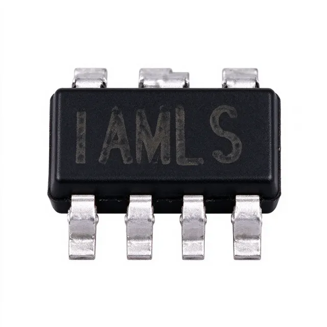
MP2451DJ-LF-Z - 36V, 2MHz, 0.6A Step-Down Converter | MPS
The Monolithic Power Systems MP2451DJ-LF-Z is a high-frequency (2 MHz) step-down switching regulator with an integrated internal high-side high-voltage power MOSFET, delivering up to 0.6 A of output current in a compact TSOT-23-6 (Thin SOT-23-6) package. It operates from a wide 3.3 V to 36 V input range and provides an adjustable output from 0.8 V, using current-mode control for fast transient loop response. A 3 µA shutdown-mode quiescent current makes the device attractive for battery-powered and always-on applications where standby drain matters. A step-down switching regulator (also called a buck converter) is a type of switched-mode power supply (SMPS) that efficiently converts a higher DC input voltage to a lower DC output voltage by rapidly switching an internal MOSFET and storing energy in an external inductor. Within the broader power-management hierarchy, the MP2451 sits between DC-DC converters (the family) and synchronous/non-synchronous buck regulators (the sub-family), making it well-suited for point-of-load (POL) rails in space-constrained designs. The 2 MHz switching frequency lets designers use a tiny 1 µH to 4.7 µH inductor, reducing total solution size dramatically versus 500 kHz alternatives. Key specifications include a 0.6 A continuous output rating, 36 V absolute-maximum input, internal compensation that removes the need for an external compensation network, and built-in protections such as over-current protection (OCP), thermal shutdown, and under-voltage lockout (UVLO). The TSOT-23-6 footprint occupies roughly 2.9 mm × 1.6 mm of board area, making the part one of the smallest 36 V-tolerant synchronous-feel buck regulators on the market. The wide VIN range specifically targets automotive and industrial environments subject to load-dump and cold-crank transients on a 12 V or 24 V bus. Typical applications include distributed 5 V or 3.3 V POL rails from a 12 V/24 V automotive battery, USB-powered devices, IoT sensors, DSL/cable modems, and portable industrial instrumentation. The combination of high switching frequency and small package also suits FPGA/CPLD auxiliary rails where board area is at a premium and low EMI from forced-CCM operation is desired. When laying out the PCB, place the input capacitor, the inductor, and the BST bootstrap component as close to the IC as possible and keep the high-current loop minimal. The exposed ground pad under the TSOT-23-6 must be soldered to a sufficient ground copper pour; the part relies on PCB copper for thermal dissipation, so a thermal via array is strongly recommended when delivering close to the 0.6 A rating continuously.
MP2949 - 3-28V Sync Buck Controller | Monolithic Power Systems
The Monolithic Power Systems MP2949 is a 3V-28V input, hysteretic synchronous step-down controller designed for high-current point-of-load conversion in distributed power architectures. Housed in a compact surface-mount QFN package with exposed thermal pad, the controller drives external high-side and low-side MOSFETs to deliver high efficiency at load currents well above what integrated FET regulators can provide. The wide 3V to 28V input range covers both 5V and 12V intermediate bus rails commonly found in telecom, computing, and industrial systems. A hysteretic control architecture is a type of switching regulator topology that uses output voltage ripple directly to trigger switching events, eliminating the need for an internal error amplifier compensation network. This results in inherently stable operation across a broad range of output LC filter combinations, very fast transient response, and simple external component selection. Hysteretic controllers trade a variable switching frequency for these benefits and are often paired with adaptive ontime variants in modern designs. Key features include programmable valley current limiting for robust overload protection, a wide 0.6V to 5V adjustable output range using an external resistor divider, internal 5V LDO for gate drive supply, and an external soft-start pin for controlled startup into large output capacitors. The exposed-pad QFN package provides a low thermal resistance path, allowing continuous operation at high load currents when properly soldered to PCB ground copper. The hysteretic control eliminates compensation network complexity, simplifying the design-in process. Typical applications include telecom base station point-of-load regulation, FPGA and ASIC core voltage generation, industrial 24V bus intermediate stages, networking switch/router power rails, and high-current DC-DC bricks for server motherboards. The 28V input tolerance also tolerates transient spikes on 24V industrial buses without additional protection circuitry. When designing with the MP2949, place the boot capacitor, bootstrap diode, and high-side MOSFET gate connection on the same PCB layer with minimal loop area to limit switching node ringing. Select the inductor ripple current at 20-40% of full load to balance transient response and conduction losses. Ensure the SNSN and SNSP current-sense traces are routed as a differential pair to reject switching node noise.

MP38876DL-LF-Z - 15A 28V Sync Buck Converter | MPS | QFN-20
The Monolithic Power Systems MP38876DL-LF-Z is a monolithic step-down (buck) switching regulator with built-in internal power MOSFETs, delivering up to 15 A continuous output current from a 4.5 V to 28 V input rail in a 20-pin QFN (3 x 4 mm) package. It integrates a synchronous gate driver for high-side and low-side MOSFETs, enabling high-frequency operation up to 400 kHz and high step-down efficiency across wide load ranges. The output voltage is adjustable down to 0.8 V, with the LF-Z suffix denoting lead-free, tape-and-reel packaging per the MPS datasheet. What is a synchronous buck converter? A buck (step-down) switching converter is a type of DC-DC voltage regulator that efficiently converts a higher input voltage to a lower output voltage by rapidly switching an internal power MOSFET and storing energy in an external inductor. Synchronous buck converters replace the traditional Schottky rectifier with a second MOSFET (synchronous rectifier) to improve efficiency, especially at high output currents. The MP38876 sits within the broader hierarchy: synchronous buck regulator -> step-down DC-DC converter -> switching voltage regulator -> power management IC. Key features include 15 A continuous output current, 4.5 V to 28 V wide operating input range, 0.8 V reference with adjustable output down to 0.6 V, internal soft-start, cycle-by-cycle over-current protection (OCP), and thermal shutdown. The device uses current-mode control that provides fast transient response and eases loop stabilization. A built-in synchronous gate driver eliminates the need for an external bootstrap circuit in many designs. The MP38876DL-LF-Z uses constant-on-time (COT) / current-mode architecture optimized for fast transient response at high step ratios. Its high switching frequency (programmable up to 400 kHz) allows the use of small external LC components, shrinking the total solution footprint. Internal MOSFETs minimize parasitic losses, while the synchronous rectifier architecture achieves high efficiency at 15 A output. This makes the MP38876 particularly well-suited for distributed POL (point-of-load) applications where board space and thermal headroom are constrained. Typical applications include distributed power systems, networking equipment, telecom base stations, industrial controllers, graphic cards, and high-current ASIC/DSP power rails. The wide VIN range also fits 12 V and 24 V industrial bus inputs commonly found in factory automation and telecom hardware. When designing with the MP38876DL-LF-Z, ensure the input capacitor and bootstrap capacitor are placed as close as possible to the IC pins. Choose an inductor with low DCR to limit conduction losses at 15 A, and verify the output capacitors have sufficient ripple current rating. The exposed pad must be soldered to a sufficient copper pour for thermal dissipation. This page synthesizes distributor pricing from Mouser and DigiKey, drop-in same-brand alternatives (MP38876DL-LF-P), and practical design notes not consolidated on the manufacturer datasheet alone.

MP4462DN-LF-Z - 3.5A 36V Step-Down Converter | Monolithic Power Systems
The Monolithic Power Systems MP4462DN-LF-Z is a 3.5 A, 4 MHz, 36 V step-down switching regulator housed in an 8-pin SOIC with exposed thermal pad. It integrates a high-side high-voltage power MOSFET and provides 3.5 A continuous output with current-mode control for fast transient response and easy external compensation, making it suitable for distributed power systems, automotive load-dump environments, and point-of-load conversion. A step-down (buck) converter is a switching DC-DC regulator that efficiently steps a higher input voltage down to a lower regulated output voltage by rapidly switching an internal MOSFET and filtering the resulting pulsed waveform through an external LC network. Within the broader power-management hierarchy, buck regulators belong to the switching-converter family, which sits alongside LDOs, charge pumps, and boost converters. Compared with linear regulators, a buck converter achieves far higher efficiency (typically >90%) because the pass element dissipates little average power, but it does introduce switching ripple and requires inductor/capacitor filtering. Key features of the MP4462DN-LF-Z include a 4.5 V to 36 V wide operating input range (with a 3.8 V minimum undervoltage lockout per the manufacturer datasheet), a fixed 4 MHz switching frequency that enables small inductors and low-EMI footprints, internal soft-start to limit inrush current, and a 120 µA (typ.) quiescent current that suits battery-connected applications. The 8-pin SOIC-8EP package exposes the die thermal pad for direct copper heatsinking, allowing full 3.5 A output at industrial temperatures. The device uses peak current-mode control, providing cycle-by-cycle current limiting and inherent input-voltage feed-forward. The high-side MOSFET is fully integrated, so only an external inductor, Schottky rectifier or low-side synchronous FET, and feedback divider are required to complete a 3.5 A point-of-load supply. According to the Monolithic Power Systems datasheet, efficiency peaks above 92% in typical 12 V-to-5 V and 12 V-to-3.3 V designs. Typical applications include 24 V industrial sensor rails, automotive infotainment and body-electronics supplies, distributed 5 V/3.3 V bus converters from 12 V or 24 V backplanes, and battery-powered equipment requiring wide input-range step-down conversion. The 4 MHz switching frequency permits use of a 1 µH to 4.7 µH inductor, ideal for space-constrained boards. When designing with the MP4462DN-LF-Z, route the feedback trace away from the switching node, place the input ceramic bypass within 2 mm of the IC, and ensure the exposed pad is soldered to a copper area of at least 1 cm² for thermal relief at full 3.5 A current. The output voltage is set from 0.8 V to ~30 V via an external resistor divider; do not exceed the 36 V absolute-maximum input. This page synthesizes distributor pricing, drop-in alternatives, and practical design notes not found in the manufacturer datasheet.

MP8009AGV-Z - 802.3af/at PoE PD Interface & Flyback Controller | MPS
The Monolithic Power Systems MP8009AGV-Z is a fully integrated IEEE 802.3af/at-compliant Power over Ethernet (PoE) powered device (PD) interface with an integrated high-efficiency flyback/forward converter controller, housed in a 28-pin QFN (4x5 mm) package. It combines a complete PD interface and a switching power supply controller in a single IC. A PoE powered device interface is the circuitry at the powered end of an Ethernet link that negotiates and receives power from a PoE switch or injector (the power sourcing equipment, PSE). Within the power management IC hierarchy, the MP8009AGV-Z belongs to the PoE powered device controller family, a subset of Power over Ethernet power interface ICs used in networking and industrial connectivity systems. Key features include full IEEE 802.3af/at functionality covering detection, 1-event and 2-event classification, a 120 mA inrush current limit, an 840 mA operational current limit, and an integrated 100 V rated hot-swap MOSFET that eliminates an external pass device. A 32 ms soft-start time gives controlled converter startup. On the converter side, the flyback/forward controller supports isolated and non-isolated PD power supply topologies, allowing designers to build the downstream DC-DC conversion stage around a single controller IC. Integration of the hot-swap MOSFET, PD interface state machine, and converter controller reduces bill-of-material count and board area compared with discrete PD interface plus separate PWM controller solutions. Typical applications include IP security cameras, wireless access points, VoIP phones, and networked industrial sensors that draw power directly over the Ethernet cable, where the MP8009AGV-Z provides PD detection, classification, inrush limiting, and isolated flyback conversion from the 48 V PoE input rail. Design consideration: verify transformer selection and feedback loop compensation against the MPS MP8009A datasheet design equations, and ensure PCB creepage on the 100 V input side meets the requirements of the target PoE class and isolation specification. This page synthesizes distributor pricing, drop-in alternative analysis, application guidance, and practical design notes not found in the manufacturer datasheet, with data verified against MPS and distributor sources as of 2026-10-19.

MP8759GD-P - 8A, 26V Sync Buck Converter | MPS
The Monolithic Power Systems MP8759GD-P is a fully integrated, high-frequency synchronous step-down (buck) switch-mode converter delivering 8A of continuous output current (10A peak) in a compact 12-pin PowerVFQFN (QFN-12) package. It accepts a wide input supply range and produces an adjustable output from 0.6V (feedback reference) up to 5.5V, with excellent load and line regulation. A synchronous buck converter (also called a step-down or DC-DC switching regulator) is a power management IC that uses integrated high-side and low-side MOSFETs, an oscillator, and a control loop to convert a higher input voltage into a lower regulated output with high efficiency. Within the power-management hierarchy, it sits between raw supply rails (such as 12V or 24V buses) and point-of-load consumers like processors, FPGAs, and memory. Key features include 8A continuous / 10A peak output current, a wide input range suited to 12V and 24V intermediate bus architectures, low quiescent current for light-load efficiency, and a high switching frequency that shrinks external inductor and capacitor sizes. MPS' proprietary control topology keeps efficiency high across a wide output-current load range, which is critical in always-on and multi-rail systems. Technically, the MP8759 integrates the power switches, gate drive, and compensation internally, offering a very compact single-inductor solution. Fixed-frequency switching operation enables predictable EMI filtering, and internal protection features such as cycle-by-cycle current limiting and thermal shutdown guard against fault conditions. Typical applications include FPGA and ASIC core/IO power rails, networking and telecom equipment point-of-load supplies, and industrial 12V/24V bus systems that need a compact high-current step-down stage. When designing with the MP8759GD-P, pay attention to PCB layout: place the input ceramic capacitors and inductor close to the IN and SW pins, and use solid ground planes to minimize the high-frequency switching loop. Verify thermal dissipation at full 8A load with the QFN-12 exposed pad soldered to a copper pour. This page synthesizes distributor pricing, drop-in alternatives, comparison data, and practical design notes not found in the manufacturer datasheet, giving engineers a one-stop selection resource.
MPM3630GQV-Z - 18V/3A Synchronous Buck Module | MPS
The Monolithic Power Systems MPM3630GQV-Z is a synchronous rectified step-down DC/DC power module with built-in power MOSFETs, inductor, and capacitors, delivering up to 3A continuous output current over a 4.5V to 18V input range. The device is housed in a compact QFN-style surface-mount module package with integrated magnetics, achieving 0.6V to 18V adjustable output with excellent load and line regulation. A DC/DC power module (also called a System-in-Package or SiP regulator) integrates the synchronous buck controller, MOSFETs, inductor, and bypass capacitors inside one LGA/QFN module. This converts the part from a discrete component kit into a near drop-in PoL (Point-of-Load) building block, reducing PCB area, BOM count, and design risk compared to a discrete buck design. The module belongs to the broader power management hierarchy: DC/DC converter > synchronous buck regulator > step-down module > integrated PoL regulator. Key features include 1.4MHz switching frequency for fast load transient response, Power Good indicator, internal soft-start, over-current protection, thermal shutdown, and under-voltage lockout. The 1.4MHz high-frequency operation allows the use of small external components while minimizing output ripple. Because the inductor is co-packaged inside the module, radiated EMI and PCB layout sensitivity are reduced compared with a discrete buck design. The MPM3630GQV-Z uses a peak-current-mode control architecture with internal compensation. Synchronous rectification eliminates the Schottky diode of older topologies and improves efficiency at light loads. The wide 4.5V-18V input range makes it compatible with 5V, 9V, 12V, and 15V system rails commonly found in industrial, networking, and FPGA/SoC applications. Typical applications include FPGA/SoC core and I/O rails, industrial control systems, telecom/datacom point-of-load regulation, distributed 12V bus architectures, and consumer electronics requiring compact high-efficiency 3A power. The wide input range simplifies integration into 12V industrial backplanes. When designing with this module, place it directly over the input/output capacitor pads and minimize the loop area of the input capacitors to the module's input pins. Because the inductor is internal, no external inductor selection is required, but adequate airflow or copper heatsinking is still required at high duty-cycle, high-output-current operation. This page synthesizes distributor pricing, verified drop-in alternatives, and practical design notes not found in the manufacturer datasheet.

MPM3682GRE - 18V 10A Step-Down Power Module QFN | MPS
The Monolithic Power Systems MPM3682GRE is a fully integrated 10 A step-down DC/DC power module that combines a synchronous buck converter, power inductor, input/output capacitors, and feedback resistors in a compact 12x12x4 mm QFN package. Operating from 4.5 V to 18 V input (or 2.5 V to 18 V with a 5 V external VCC bias), it delivers an adjustable output from 0.65 V to 5 V with up to 10 A of continuous load current at 500 kHz switching frequency. Background Knowledge: A Point-of-Load (PoL) DC/DC converter is a non-isolated switching regulator placed physically close to the load it powers (typically a processor, ASIC, or FPGA). Within the broader power management hierarchy, a PoL module sits between the intermediate bus converter and the load ICs, providing tight, fast-responding local rails. Fully integrated modules such as the MPM3682GRE differ from discrete buck designs because the high-di/dt power loop (high-side FET, low-side FET, inductor, and input/output bypass capacitance) is contained inside the package, simplifying PCB layout, reducing radiated EMI, and shrinking total solution footprint. Key features include Constant-On-Time (COT) control for fast transient response, simple loop compensation that requires no external RC network, and a solution that needs as few as two external components (one resistor and one capacitor) to operate. Built-in protections include over-current, over-voltage, under-voltage, and over-temperature shutdown. The 12x12x4 mm QFN package exposes a thermal pad that enables direct PCB heat-sinking through the inner power planes. Technical depth: COT control uses the output ripple as part of the PWM ramp, eliminating the need for a closed-loop compensation network in most applications. This architecture achieves sub-microsecond transient response compared with classical voltage-mode or current-mode control, and it scales cleanly to multi-phase or stacked configurations when higher currents are required. Internal MOSFETs and the shielded inductor confine the noisy switching node, keeping the module's radiated EMI signature well below that of a comparable discrete buck. Typical applications include telecom baseband and FPGA core rails, industrial 12 V intermediate-bus POLs, networking switches and routers, server aux rails, and graphics/embedded computing subsystems. The wide 4.5 V-18 V input range covers both 5 V and 12 V intermediate-bus standards, while the 0.65 V-5 V output range supports legacy and modern logic rails from 1.x V cores up to 5 V analog supplies. When designing with this device, place the single feedback resistor and the optional soft-start capacitor immediately adjacent to the FB and SS pins. The exposed pad must be soldered to a continuous ground copper pour with multiple thermal vias to keep junction temperature within ratings at full 10 A load; derate output current linearly above 65 deg C ambient. This page synthesizes distributor pricing, application-ready alternatives, and PCB-level design guidance not bundled in the manufacturer datasheet.
MPM54304GMN-0000 - Quad 3A/3A/2A/2A PMIC Module | MPS
The Monolithic Power Systems MPM54304GMN-0000 is a complete quad-output power management module that integrates four high-efficiency synchronous step-down DC/DC converters, inductors, and a flexible I2C/MTP-programmable logic interface in a single 33-pin PowerFLGA (ultra-thin LGA) package. Operating from a 4V to 16V input, the device delivers configurable output currents of 3A, 3A, 2A, and 2A (with channel 1+2 parallelable to 6A and channel 3+4 parallelable to 4A) across an adjustable output range of 0.55V to 7V, with constant-on-time (COT) control providing ultra-fast load transient response. The module embeds auto-compensation, eliminating the external compensation network that conventional buck converters require. A power management module is a higher-level integration than a discrete DC/DC converter IC: in addition to the controller and FETs, the module embeds the power inductors and most passive components, shrinking the PCB footprint, reducing BOM count, and simplifying layout for multi-rail systems. Within the broader power-management taxonomy, the MPM54304 sits between a point-of-load (POL) regulator and a system PMIC — combining PMIC-style multi-rail programmability with POL-style efficiency and density. The package_svg_key used for the on-page diagram is the 33-pin LGA representation. Key features include I2C digital interface for output-voltage, sequencing, and fault-mask programming; MTP (multi-time programmable) non-volatile memory for storing default configuration; adjustable switching frequency from 500 kHz to 1.6 MHz; power-good indicators per channel; and protection features including OCP, OVP, UVP, and thermal shutdown. According to the MPS datasheet, the COT architecture eliminates the need for loop compensation and enables fast transient response without overshoot. Typical applications include FPGA and SoC core/IO/auxiliary rail generation (the MPS reference design is centered on AMD Zynq-7000), compact industrial control boards, machine-vision cameras, IoT gateways, and any space-constrained multi-rail system where PCB area is at a premium. The 16V maximum input supports 12V bus systems directly. When designing with the MPM54304GMN-0000, follow the MPS EVM54304-MN-01A reference layout for input/output capacitor selection and thermal copper. Place input bulk capacitors within 3 mm of the module. Output voltage setting via I2C overrides the external feedback resistor only after MTP configuration is written. The ultra-thin package requires careful PCB warpage control during reflow.
MPM54304GMN-0001 - 4V-16V Quad-Output PMIC 3A/3A/2A/2A | MPS
The Monolithic Power Systems MPM54304GMN-0001 is a quad-output power module that integrates four high-efficiency synchronous step-down DC/DC converters, integrated inductors, and a flexible I2C/MTP logic interface in a 33-pin PowerFLGA (LGA-33, 7x7x2 mm) package. It accepts an input voltage of 4 V to 16 V and delivers four independently adjustable outputs of 3 A, 3 A, 2 A, and 2 A over an output range of 0.55 V to 7 V at a default 1.5 MHz switching frequency. According to the manufacturer datasheet, the module achieves fast transient response through constant-on-time (COT) control with internal auto-compensation, eliminating the need for an external compensation network. A Power Management IC (PMIC) is a highly integrated voltage regulator that consolidates multiple DC/DC and LDO rails into a single package to power processors, FPGAs, and SoCs. In the system hierarchy, a PMIC sits below a discrete buck converter and above a simple LDO, occupying the role of complete subsystem power management; the MPM54304 specifically belongs to the quad-output, high-current, point-of-load PMIC subcategory. The MPM54304GMN-0001's output voltage can be set via I2C or by an external resistor divider, and the MTP (multi-time programmable) memory allows factory customization of default voltages, sequence, and timing for each rail. Key features include four synchronous step-down converters in a single ultra-thin 2 mm module, internal compensation, constant-on-time control with fast load-step response, I2C-configurable output voltages and fault thresholds, MTP-programmable defaults, integrated soft start, and full protection (OCP, OVP, UVP, OTP). The switching frequency is factory-set to 1.5 MHz by default, allowing the use of small ceramic input and output capacitors and minimizing PCB area compared with discrete buck solutions that require external inductors and compensation components. Typical applications include FPGA/SoC power for AMD Zynq-7000 family and similar MPSoCs, multi-rail industrial automation boards, compact networking switches, point-of-load regulation for PCIe cards, and any dense PCB that previously required four discrete buck converters with inductors. The module replaces at least eight to twelve discrete components per board, reducing BOM count, layout complexity, and EMI risk from separate inductor loops. When designing with this device, ensure that the 4 V to 16 V input range is respected, route the AGND/DGND return as a single-star ground, and place the bootstrap capacitors as close as possible to the BST pins. For non-I2C designs, the SCL/SDA pins must be terminated per the manufacturer's forum guidance (typically pulled up or grounded as documented), and the output resistor divider must use 1% resistors for set-point accuracy.
MPQ2167BGDE-AEC1-P - 6V, 4A Sync Buck Converter, AEC-Q100 | MPS
The Monolithic Power Systems MPQ2167BGDE-AEC1-P is a frequency-programmable, AEC-Q100-qualified synchronous step-down (buck) converter that delivers up to 4 A of continuous output current from a 2.7 V to 6.0 V input rail, packaged in an 11-pin PowerVQFN module with wettable flanks. The output voltage is adjustable down to 0.606 V using an external resistor divider, and the switching frequency is configurable from 300 kHz to 2.2 MHz through an external resistor, allowing the designer to trade efficiency against solution size. Peak-current-mode control provides excellent transient response and simplifies loop compensation across the wide switching-frequency range. A buck converter (also called a step-down switching regulator) is a switch-mode DC-DC converter topology that uses an internal high-side MOSFET, an external or integrated low-side MOSFET, an inductor, and output capacitors to efficiently reduce a higher DC input voltage to a lower regulated output voltage. Within the broader product hierarchy, this part belongs to the synchronous-buck family of voltage regulators, which sits inside the DC-DC switching regulator category, inside the power management IC family, inside the semiconductor category. Synchronous designs replace the traditional Schottky rectifier with a low-side MOSFET, raising light-load efficiency and reducing conduction losses - critical in 3.3 V and 5 V point-of-load applications. Key features of the MPQ2167BGDE-AEC1-P include 4 A continuous output current, 2.7 V to 6.0 V input range, 0.606 V minimum output, 300 kHz to 2.2 MHz programmable switching frequency, internal power MOSFETs, AEC-Q100 Grade 1 qualification for automotive environments, and a wettable-flank PowerVQFN package that supports automated optical inspection of solder joints. The wide frequency range and small solution footprint suit space-constrained automotive infotainment, ADAS sensor rails, and industrial point-of-load designs. Typical applications include automotive infotainment and cluster power rails, ADAS camera/sensor power, industrial PLC and factory-automation logic rails, USB-PD and 5 V point-of-load regulation, FPGA/SoC core and I/O supplies, and portable battery-powered equipment. The AEC-Q100 qualification makes it particularly attractive for under-the-hood and body-electronic modules subject to wide temperature swings. When designing with this device, place the input ceramic capacitors immediately adjacent to the VIN and PGND pins to minimize switching-node ringing, and choose the inductor such that peak-to-peak ripple current stays around 30% of the load. Estimate: at 4 A load, 600 kHz fsw, and 3.3 V VOUT, a 1.5 uH inductor gives roughly 0.45 A ripple. A 2-layer PCB with a continuous ground plane is recommended for thermal dissipation. This page synthesizes distributor pricing, drop-in alternatives, and practical design notes not found in the manufacturer datasheet alone.

MPQ2908AGF-AEC1 - 60V Sync Step-Down Controller, AEC-Q100 | MPS
The Monolithic Power Systems MPQ2908AGF-AEC1 is an AEC-Q100 qualified, 4V to 60V input, current-mode synchronous step-down switching controller housed in a 20-pin TSSOP-20EP (Exposed Pad) package. It directly steps down high-voltage rails such as automotive 12V/24V buses and industrial 48V systems to logic-level outputs with high efficiency. The controller drives dual N-channel MOSFETs in a synchronous buck topology with accurate cycle-by-cycle current limiting. A synchronous step-down controller (buck controller) is a type of DC-DC switching regulator that uses an external pair of MOSFET switches and an LC output filter to convert a higher input voltage to a lower regulated output voltage. It sits in the power management IC family, between discrete switching regulators and fully integrated synchronous buck ICs, and is preferred when output current exceeds the capability of monolithic converters. The MPQ2908A family targets wide-Vin, high-current automotive and industrial rails where a controller plus external MOSFETs gives designers flexibility on current, RDS(on), and thermal budget. Key features include a wide 4V to 60V operating input range, current-mode PWM control with cycle-by-cycle over-current protection, an Advanced Asynchronous Mode (AAM) for improved light-load efficiency, and AEC-Q100 Grade qualification for automotive environments. The TSSOP-20EP exposed pad offers a low thermal resistance path to PCB copper for dissipating controller-side losses. Built-in protection features include OCP, OVP, UVLO, and thermal shutdown. The architecture uses peak current-mode control with internal slope compensation, providing excellent line-transient response and simple single-loop compensation. The MPQ2908AGF-AEC1 supports both continuous-conduction synchronous operation at heavy loads and diode-emulation AAM at light loads to reduce switching losses. An external SS/TRK pin sets soft-start and tracking behavior for sequencing in multi-rail systems. Typical applications include automotive infotainment and ADAS power rails, 24V industrial sensor and PLC supplies, battery-powered e-mobility systems (48V e-bike, forklift, light EV), telecom 48V backplane POL conversion, and point-of-load regulators in distributed 24V industrial racks. The wide Vin and AEC-Q100 grade make it a strong fit for any 12V/24V/48V bus system. When designing with this controller, select external MOSFETs rated for the application's maximum load current and Vin transients (load-dump tolerant up to 60V), and choose the inductor such that ripple current is roughly 30% of full load. Place the input/bootstrap capacitors close to the SW and BST pins to minimize switching-node parasitic inductance and ringing. For automotive designs, follow MPS's EMI mitigation layout note for two-layer boards.
MPQ3431AGL-AEC1-Z - 21A Synchronous Boost Converter | MPS | AEC-Q100
The Monolithic Power Systems MPQ3431AGL-AEC1-Z is a 21 A high-efficiency fully-integrated synchronous boost converter with configurable input current limit, housed in a 13-pin PowerVFQFN (QFN-13 3x4 mm) package and AEC-Q100 qualified for automotive applications. A boost converter (also called a step-up converter) is a switching DC-DC power topology that produces an output voltage higher than its input voltage by storing energy in an inductor during the switch-on phase and releasing it into the load during the switch-off phase. Synchronous boost converters replace the conventional Schottky rectifier with a low-side MOSFET, which dramatically reduces conduction losses and improves efficiency at high output currents. The MPQ3431A occupies the power management IC (PMIC) tier within the DC-DC switching regulator family, which itself sits under the broader power management umbrella for battery-powered and automotive electrical systems. Key headline specifications include a 21 A switch current capability, a fixed 450 kHz switching frequency, a wide 2.7 V to 13 V start-up input range, an adjustable output voltage from 0.8 V upward, and a selectable MODE pin that allows the user to choose pulse-skip mode (PSM), forced continuous conduction mode (FCCM), or ultrasonic mode (USM) under light-load conditions. The integrated low-side MOSFET also handles cycle-by-cycle inductor peak current limiting, eliminating the need for an external sense resistor. The device adopts constant-off-time (COT) control topology, which provides fast transient response to load steps - a critical advantage over traditional voltage-mode or current-mode PWM controllers in automotive load-dump and cold-crank scenarios. The configurable input current limit provides accurate overload protection from a misbehaving upstream supply, while the high-side and low-side MOSFET integration simplifies PCB layout and reduces bill-of-materials cost. The 3 mm x 4 mm PowerVQFN package with an exposed thermal pad supports continuous high-current operation with proper PCB thermal design. Typical applications include automotive front-camera power, infotainment USB-PD rails, eCall backup supplies, ADAS sensor biasing, and 12 V battery-to-boosted rails for audio amplifiers. The AEC-Q100 Grade 1 qualification makes the part especially suitable for under-hood and safety-relevant automotive subsystems. Designers should pay particular attention to inductor selection - the constant-off-time topology with a 450 kHz nominal frequency pair well with 1-3 µH power inductors rated for at least 25 A saturation current. The MODE pin must be tied high, low, or left floating according to the desired light-load behavior. This page synthesizes distributor pricing, parametric drop-in alternatives, and practical design notes that go beyond the manufacturer datasheet to accelerate automotive power design.

MPQ4420-AEC1 - 2A 36V Sync Buck Converter | MPS | Automotive
The Monolithic Power Systems MPQ4420-AEC1 is an automotive-grade, high-efficiency synchronous step-down (buck) switch-mode converter with built-in power MOSFETs, delivering up to 2A of continuous output current from a wide input supply range up to 36V maximum, packaged in a space-saving 8-pin TSOT23-8 (SOT-23-8 Thin, TSOT-23-8) surface-mount package with power-good (PG) indication and external synchronization support. A synchronous buck converter is a type of DC-DC switching regulator that uses two internal MOSFETs - a high-side switch and a low-side synchronous rectifier - instead of a Schottky diode, reducing conduction losses and raising efficiency across the load range. Within the power-management hierarchy, the MPQ4420-AEC1 sits in the step-down converter family of switching regulators, part of a broader power supply IC chain that converts a higher unregulated input voltage into a tightly regulated lower output voltage. Key differentiating features include a 2A continuous output current rating with excellent load and line regulation over a wide input supply range, an output voltage adjustable down from 0.8V (the feedback reference), current-mode control, and AEC-Q100 Grade 1 automotive qualification. Protection features include cycle-by-cycle over-current protection with hiccup-mode restart, and thermal shutdown. Architecturally, the MPQ4420 uses current-mode operation, which provides fast transient response and eases loop stabilization compared with voltage-mode control. Synchronous rectification maintains high efficiency from light load to full 2A load. When the inductor current peak exceeds the set current limit and the feedback voltage falls below the under-voltage threshold (typically 84% below the reference), the part enters hiccup mode and periodically restarts, protecting the converter during short-circuit faults. Typical applications include automotive power systems (the -AEC1 suffix denotes AEC-Q100 qualified automotive grade), industrial auxiliary power rails from 12V/24V buses, and distributed point-of-load regulation where a compact, minimal-external-component buck solution is required. A key design consideration is thermal and layout discipline: with an integrated MOSFET buck in a TSOT23-8 package, keep the input ceramic capacitor and inductor loops tight and provide adequate copper area on SW and GND for heat dissipation at high input-to-output voltage ratios. This page synthesizes verified datasheet data, drop-in family alternatives, comparison tables, and practical design notes not found together on distributor listing pages.