LIN Transceivers
بەرهەمەکان (28)

ADM3050EBRWZ-RL7 - 5.7kV Isolated CAN FD Transceiver | Analog Devices
The ADM3050EBRWZ-RL7 is a 5.7 kV rms isolated controller area network (CAN) physical layer transceiver with a high performance, basic feature set, manufactured by Analog Devices. It integrates a 2-channel digital isolator and a CAN transceiver into a single 16-lead SOIC package using Analog Devices' iCoupler technology. The device fully meets the CAN flexible data rate (CAN FD) ISO 11898-2:2016 requirements and supports data rates up to 12 Mbps, making it suitable for industrial and automotive networking applications. A CAN transceiver is a device that provides the physical layer interface between a CAN controller and the differential bus lines. It converts the digital signals from the controller into differential signals for transmission over the twisted-pair bus and vice versa. In isolated CAN transceivers, galvanic isolation is provided between the controller side and the bus side to protect against ground potential differences, noise, and transient voltages. The ADM3050E belongs to the family of isolated CAN transceivers, which are essential in harsh environments where safety and reliability are critical. Key features of the ADM3050EBRWZ-RL7 include 5.7 kV rms isolation voltage, integrated DC-to-DC converter for isolated power, and compliance with ISO 11898-2:2016. It supports CAN FD data rates up to 12 Mbps, ensuring high-speed communication. The device also passes EN 55022 Class B radiated emissions by 6 dB on a simple 2-layer PCB, eliminating the need for stitching capacitance or high-voltage SMT safety capacitors. This simplifies PCB layout and reduces BOM cost. Technically, the ADM3050E employs iCoupler technology, which uses chip-scale transformers to provide isolation, offering superior performance compared to optocouplers in terms of speed, reliability, and power consumption. The integrated DC-to-DC converter provides isolated power to the bus side, eliminating the need for an external isolated power supply. The device operates over a wide temperature range and includes thermal shutdown and current limiting protection. Typical applications include industrial fieldbus networks, building automation, motor control, and automotive electronics. The high isolation voltage and robust EMC performance make it ideal for systems where ground loops and noise are concerns. The ADM3050EBRWZ-RL7 is available in tape and reel packaging, suitable for high-volume production. When designing with this device, ensure proper PCB layout to maintain isolation creepage and clearance distances. The integrated DC-to-DC converter requires careful placement of external components to minimize noise. Refer to the ADM3050E datasheet for detailed application information.

ADM3051BRWZ - High Speed Industrial CAN Transceiver | Analog Devices
The ADM3051BRWZ is a high-speed industrial Controller Area Network (CAN) physical layer transceiver from Analog Devices. It operates from a 5 V supply (VCC) and complies with the ISO 11898 standard, enabling data rates up to 1 Mbps. The device is housed in a 14-lead SOIC (BRWZ) package and is designed for robust industrial communication, supporting connection of 110 or more nodes on a single bus. Key features include short-circuit protection on CANH and CANL against shorts to power or ground in 24 V systems, slope control for reduced EMI, thermal shutdown protection, and a low current standby mode. Unpowered nodes do not disturb the bus, ensuring system reliability during power cycling. A CAN transceiver is a physical layer device that interfaces between a CAN protocol controller and the differential bus lines (CANH and CANL). It converts the digital signals from the controller into differential signals for transmission over the twisted-pair bus and vice versa. The transceiver is a critical component in the CAN network hierarchy, which spans from the application layer down to the physical layer. The ADM3051BRWZ specifically implements the physical layer, providing the necessary drive strength, receiver sensitivity, and protection features required for robust communication in harsh industrial environments. Key features of the ADM3051BRWZ include its compliance with ISO 11898, which ensures interoperability with other standard CAN devices. The device supports data rates up to 1 Mbps, making it suitable for high-speed industrial control applications. Its short-circuit protection on CANH and CANL against shorts to power or ground in 24 V systems enhances robustness in industrial settings where wiring faults are common. The slope control feature allows the designer to reduce electromagnetic interference (EMI) by controlling the slew rate of the output signals, which is particularly useful in applications with stringent EMC requirements. Thermal shutdown protection prevents damage from excessive power dissipation, and the low current standby mode reduces power consumption when the bus is idle. From a technical perspective, the ADM3051BRWZ is designed to handle the electrical stresses of industrial environments. Its differential output voltage and receiver input sensitivity are optimized for reliable communication over long bus lengths (up to 1 km) and with many nodes. The device's common-mode input range accommodates ground potential differences between nodes, which is common in distributed systems. The transceiver's propagation delay and loop delay are carefully controlled to ensure timing compliance with the CAN protocol, even at 1 Mbps. The device also features a silent mode (via the RS pin) that disables the transmitter, allowing for bus monitoring without driving the bus. Typical applications for the ADM3051BRWZ include industrial automation, building automation, automotive electronics (non-safety critical), and any system requiring robust CAN communication. In industrial automation, it is used in PLCs, sensors, and actuators to provide reliable data exchange over long distances. In building automation, it enables communication between HVAC controllers, lighting systems, and access control panels. The device's high-speed capability and robustness make it ideal for these applications. When designing with the ADM3051BRWZ, it is important to consider proper bus termination (typically 120 ohms at each end) and to use twisted-pair cabling to minimize EMI. The slope control pin (RS) can be used to adjust the slew rate for EMI reduction, but this also limits the maximum data rate. For 1 Mbps operation, the slope control should be set to high-speed mode (RS connected to ground). Additionally, the VCC supply should be decoupled with a 100 nF capacitor close to the VCC pin to ensure stable operation.
ADM3052BRWZ - Isolated CAN Transceiver with Regulator | Analog Devices
The ADM3052BRWZ from Analog Devices is an isolated controller area network (CAN) physical layer transceiver with an integrated high-voltage, bus-side linear regulator. It complies with the ISO 11898 standard and employs iCoupler® technology to combine a 3-channel isolator, a CAN transceiver, and a linear regulator in a single 16-lead SOIC-W package. The device supports data rates up to 1 Mbps and operates from a 3.3V or 5V logic-side supply, while the bus-side regulator accepts inputs from 5V to 27V, providing a regulated 5V output for the bus-side circuitry. An isolated CAN transceiver is a component that provides galvanic isolation between the CAN protocol controller and the physical bus, protecting the logic side from high common-mode voltages, ground loops, and electrical noise. It integrates a digital isolator, a CAN transceiver, and often a DC-DC converter or regulator to power the isolated side. In the hierarchy of CAN interface components, it sits above a standard transceiver by adding isolation, which is critical in industrial, automotive, and building automation systems where long bus lengths and differing ground potentials are common. Key features include a 5 kVrms isolation rating, a bus-side linear regulator with 5V output, and compliance with ISO 11898-2. The device offers a common-mode voltage range of -12V to +12V and a common-mode transient immunity of 25 kV/µs, ensuring robust operation in noisy environments. It also features thermal shutdown protection and a logic-side supply range of 3.0V to 5.5V, making it versatile for various controller interfaces. Technically, the ADM3052 integrates a 3-channel iCoupler digital isolator for the TXD, RXD, and a control signal, eliminating the need for a separate isolation barrier. The integrated linear regulator simplifies power supply design by generating the isolated 5V bus supply from a higher input voltage, reducing component count and board space. The device is specified for the industrial temperature range of -40°C to +85°C and is available in a 16-lead SOIC-W package. Typical applications include industrial fieldbus networks, building automation systems, automotive diagnostics, and any CAN bus requiring galvanic isolation. The integrated regulator is particularly useful in systems where a 24V supply is available, as it can directly power the bus side without an external DC-DC converter. When designing with the ADM3052, ensure proper PCB layout with adequate creepage and clearance for the isolation barrier, and place decoupling capacitors close to the VCC and V+ pins. The bus-side regulator requires an output capacitor for stability, and the input voltage must not exceed the absolute maximum rating of 27V.

ADM3053BRWZ - Isolated CAN Transceiver with isoPower | Analog Devices
The ADM3053BRWZ from Analog Devices is a signal and power isolated controller area network (CAN) physical layer transceiver with an integrated isolated DC-to-DC converter. It combines a 2-channel isolator, a CAN transceiver, and Analog Devices isoPower DC-to-DC converter into a single 20-lead SOIC surface mount package. The device complies with the ISO 11898 standard and supports high-speed data rates up to 1 Mbps. It operates with a 5 V supply on VCC and either 5 V or 3.3 V on VIO, providing flexibility for interfacing with different logic levels. The ADM3053BRWZ features 2.5 kV rms signal and power isolation, making it ideal for applications requiring galvanic isolation in industrial, automotive, and instrumentation systems. An isolated CAN transceiver is a device that provides the physical layer interface between a CAN controller and the differential bus, while also providing electrical isolation between the two sides. This isolation protects the low-voltage logic side from high-voltage transients, ground loops, and common-mode noise that can occur on the bus. The integration of an isolated DC-to-DC converter eliminates the need for a separate isolated power supply, simplifying design and reducing board space. The ADM3053BRWZ is part of the broader family of isolated interface ICs, which includes isolated RS-485 transceivers and isolated digital isolators, all leveraging Analog Devices' iCoupler technology. Key features of the ADM3053BRWZ include its compliance with ISO 11898, high-speed data rates up to 1 Mbps, and the ability to connect 110 or more nodes on the bus. It also offers slope control for reduced EMI, thermal shutdown protection, and high common-mode transient immunity. The device supports unpowered nodes, meaning that nodes without power do not disturb the bus, which is critical for fault-tolerant systems. The integrated isoPower DC-to-DC converter provides up to 500 mW of isolated power, which can be used to power the transceiver itself or external circuitry on the isolated side. Technically, the ADM3053BRWZ uses iCoupler technology to achieve isolation, which uses chip-scale transformers to transmit data and power across the isolation barrier. This approach provides reliable isolation with high data rates and low power consumption compared to traditional optocoupler-based solutions. The device also features an internal split paddle lead frame on the bus side, which helps with thermal management and reduces parasitic inductance. The operating temperature range is -40°C to +125°C, making it suitable for harsh environments. Typical applications include industrial fieldbus networks, building automation, automotive diagnostics, and medical equipment. In industrial automation, the ADM3053BRWZ is used to connect sensors and actuators to a CAN bus while providing isolation to protect the control system from electrical noise. In automotive applications, it is used for in-vehicle networking and diagnostics, where isolation is required to prevent ground loops and protect sensitive electronics. When designing with the ADM3053BRWZ, it is important to place a low inductance ceramic capacitor close to the VCC and VIO pins, with the total lead length between the capacitor and the power supply pin not exceeding 10 mm. This ensures stable operation and minimizes noise. Additionally, the bus side should be properly terminated to match the characteristic impedance of the bus to prevent signal reflections.

ADM3053BRWZ-RL7 - Isolated CAN Transceiver with isoPower | Analog Devices
The ADM3053BRWZ-RL7 is a signal and power isolated CAN (Controller Area Network) physical layer transceiver with an integrated isolated DC-to-DC converter, manufactured by Analog Devices. It complies with the ISO 11898 standard and is available in a 20-lead wide-body SOIC package. The device operates from a single 5 V supply on VCC and supports 5 V or 3.3 V operation on VIO, enabling interface to different logic levels. It provides 2.5 kV rms signal and power isolation, making it suitable for industrial and automotive applications where galvanic isolation is required. A CAN transceiver is a device that interfaces between a CAN controller and the physical bus, providing differential transmit and receive capabilities. The ADM3053 integrates the transceiver with an isolated DC-to-DC converter using Analog Devices' iCoupler and isoPower technologies, eliminating the need for a separate isolated power supply. This integration reduces PCB footprint and simplifies design, as the device provides fully isolated power and data in a single package. Key features include high-speed data rates up to 1 Mbps, support for connecting 110 or more nodes on the bus, slope control for reduced EMI, thermal shutdown protection, and high common-mode transient immunity. The integrated isoPower converter uses high-frequency switching elements to transfer power through an internal transformer, requiring careful PCB layout to meet emissions standards. The ADM3053 is fully specified over the industrial temperature range and is available in a 20-lead wide-body SOIC package. It is designed for harsh environments where noise immunity and isolation are critical. The device's unpowered nodes do not disturb the bus, ensuring reliable operation in multi-node networks. Typical applications include industrial automation, building automation, automotive electronics, and any system requiring isolated CAN communication. The integrated isolation simplifies design and reduces component count, making it ideal for space-constrained applications. When designing with the ADM3053, special attention must be paid to PCB layout to minimize emissions from the isoPower converter. Following the manufacturer's layout guidelines is essential for meeting EMC standards.
ADM3054BRWZ - 5kVrms Isolated CAN Transceiver | Analog Devices
The ADM3054BRWZ is a 5 kV rms signal isolated controller area network (CAN) physical layer transceiver from Analog Devices. It integrates a 3-channel digital isolator and a CAN transceiver using Analog Devices' iCoupler technology, providing a complete isolated CAN solution in a 16-lead SOIC package. The device complies with the ISO 11898 standard and supports data rates up to 1 Mbps, making it suitable for industrial and automotive CAN networks. A CAN transceiver is a device that interfaces between the CAN controller (e.g., a microcontroller with built-in CAN) and the physical differential bus. It converts the digital logic levels of the controller to the differential voltages required on the CAN bus and vice versa. Isolation is critical in harsh environments to protect the controller and users from high voltages, ground loops, and noise. The ADM3054 provides galvanic isolation up to 5 kV rms, ensuring safe and reliable communication in industrial automation, motor control, and electric vehicle applications. Key features include 5 kV rms isolation, integrated DC-to-DC converter (for the BRWZ variant, it includes an integrated isolated power supply), bus protection up to ±58 V, and thermal shutdown. The device operates from a single 5 V supply on the logic side and a 5 V or 3.3 V supply on the bus side, with a typical data rate of 1 Mbps. It also features a high common-mode transient immunity of 25 kV/µs, ensuring robust operation in noisy environments. The ADM3054 uses iCoupler technology, which uses chip-scale transformers to isolate signals, providing superior performance compared to optocouplers in terms of speed, power consumption, and reliability. The integrated DC-to-DC converter eliminates the need for an external isolated power supply, simplifying design and reducing board space. The device also includes a VIO pin for logic-level translation, allowing interface with 3.3 V or 5 V microcontrollers. Typical applications include industrial fieldbus networks, motor control, HVAC systems, electric vehicle charging, and battery management systems. The high isolation voltage and robust bus protection make it ideal for applications where safety and reliability are paramount. When designing with the ADM3054BRWZ, ensure proper PCB layout with adequate creepage and clearance distances for the isolation barrier. Place decoupling capacitors close to the VCC and VIO pins, and follow the recommended layout in the datasheet to achieve the specified isolation performance.
ADM3054BRWZ-RL7 - 5kVrms Isolated CAN Transceiver | Analog Devices
The ADM3054BRWZ-RL7 is a 5 kV rms signal isolated controller area network (CAN) physical layer transceiver from Analog Devices. It integrates a 3-channel digital isolator and a CAN transceiver into a single 16-pin SOIC-W package using Analog Devices' iCoupler technology. The device complies with the ISO 11898 standard and supports data rates up to 1 Mbps, making it suitable for industrial and automotive CAN bus applications. A CAN transceiver is a device that provides the physical layer interface between a CAN controller and the differential bus lines. It converts the digital signals from the controller into differential signals for transmission over the twisted-pair bus and vice versa. The ADM3054 adds galvanic isolation, protecting the logic side from high voltages and ground loops on the bus side, which is critical in harsh industrial environments. Key features include 5 kV rms isolation voltage, a wide supply range of 3.3 V or 5 V on the logic side (VDD1) and 5 V on the bus side (VDD2), and a data rate of up to 1 Mbps. The device also features bus protection against short circuits and thermal shutdown, ensuring robust operation. The SOIC-16 package provides a compact footprint for space-constrained designs. The ADM3054 uses iCoupler technology, which employs chip-scale transformers to provide isolation, eliminating the need for optocouplers and external components. This results in higher reliability, lower power consumption, and better timing accuracy compared to traditional isolation methods. The device also includes a VREF output for bus biasing and a silent mode for listen-only operation. Typical applications include industrial fieldbus networks, motor control systems, building automation, and automotive body electronics. The high isolation rating and compliance with ISO 11898 make it ideal for systems requiring robust communication in noisy environments. When designing with the ADM3054, ensure proper PCB layout with adequate creepage and clearance distances for the isolation barrier. Place decoupling capacitors close to the VDD1 and VDD2 pins, and consider the thermal dissipation of the device under high data rates.
ADM3055EBRWZ - 5kV Isolated CAN FD Transceiver | Analog Devices
The ADM3055EBRWZ is a 5 kV rms signal and power isolated CAN transceiver with an integrated isoPower DC-to-DC converter, designed for CAN FD networks. It combines a 3-channel iCoupler isolator, a CAN transceiver, and an isolated DC-to-DC converter into a single 20-lead SOIC-W package, enabling a fully isolated CAN solution powered from a single 5 V supply. A CAN transceiver is the physical layer interface between a CAN controller and the differential bus lines (CANH and CANL). It converts the controller's logic-level signals to differential signals for transmission and receives differential signals back to logic levels. In industrial and automotive environments, galvanic isolation is often required to protect controllers from ground loops, voltage transients, and noise. The ADM3055E integrates this isolation, eliminating the need for external isolation components and simplifying PCB design. Key features include 5 kV rms isolation, compliance with ISO 11898-2:2016 for CAN FD, data rates up to 12 Mbps, a VIO pin for 1.7 V to 5.5 V logic levels, extended common-mode range of ±25 V, and bus fault protection of ±40 V on CANH and CANL pins. The device also supports low-power standby with remote wake request, making it suitable for power-sensitive nodes. The ADM3055E uses Analog Devices' iCoupler and isoPower technologies, which use chip-scale transformers to transmit data and power across the isolation barrier. This approach provides reliable isolation with low propagation delay (150 ns maximum loop) and high common-mode transient immunity. The integrated DC-to-DC converter eliminates the need for a separate isolated power supply, reducing component count and board space. Typical applications include industrial fieldbus networks, building automation, automotive diagnostics, and any system requiring robust, isolated CAN communication. The wide logic-level range and high data rate make it versatile for both legacy CAN and newer CAN FD designs. When designing with this device, ensure proper PCB layout for the isolation barrier and provide adequate decoupling on both the logic and bus sides. The integrated converter requires careful thermal management at high data rates and loads.
ADM3055EBRWZ-RL7 - 5kV Isolated CAN Transceiver | Analog Devices
The ADM3055EBRWZ-RL7 is a 5 kV rms signal and power isolated CAN transceiver with an integrated isoPower isolated DC-to-DC converter, designed for CAN FD networks. It complies with the ISO 11898-2:2016 standard and supports data rates up to 12 Mbps, making it suitable for industrial and automotive applications requiring robust, isolated communication. The device is available in a 16-lead SOIC-W package and operates over a wide temperature range. A CAN transceiver is a physical layer device that connects a CAN controller to the differential bus lines (CANH and CANL). It converts the digital signals from the controller into differential signals for transmission and vice versa. Isolation in a CAN transceiver provides galvanic isolation between the bus side and the logic side, protecting sensitive electronics from ground loops, voltage spikes, and noise. The ADM3055E integrates the isolation barrier and DC-to-DC converter, eliminating the need for external isolated power supplies. Key features include 5 kV rms isolation, an integrated isolated DC-to-DC converter, a VIO pin for 1.7 V to 5.5 V logic levels, low maximum loop propagation delay of 150 ns, extended common-mode range of ±25 V, and bus fault protection of ±40 V on CANH and CANL pins. It also supports low power standby with remote wake, making it ideal for power-sensitive nodes. The ADM3055E uses Analog Devices' isoPower technology, which integrates a DC-to-DC converter with the signal isolation, providing a complete isolated CAN solution in a single package. This reduces board space and component count compared to discrete isolation solutions. The device is designed to meet the stringent requirements of CAN FD, ensuring reliable communication at high data rates. Typical applications include industrial automation, building automation, motor control, and automotive electronics. The integrated isolation and DC-to-DC converter simplify design and improve reliability in harsh environments. The device is also suitable for battery management systems and other applications requiring isolated CAN communication. When designing with the ADM3055E, ensure proper PCB layout for the isolation barrier and provide adequate decoupling on the VIO and VCC pins. The integrated DC-to-DC converter requires careful consideration of the external components, such as the transformer and rectifier, to achieve optimal performance.

ISO1042 - Isolated CAN Transceiver with 70V Fault Protection | TI
The Texas Instruments ISO1042 is a galvanically-isolated controller area network (CAN) transceiver that meets the specifications of the ISO11898-2 (2016) standard. It offers ±70V DC bus fault protection and ±30V common-mode voltage range, making it robust for industrial and automotive networking. The device supports data rates up to 5 Mbps in CAN FD mode, enabling faster payload transfer compared to classic CAN. It is available in an 8-pin SOIC (DW) package and operates over a wide temperature range. A CAN transceiver is a physical-layer device that interfaces between the CAN protocol controller and the differential bus lines. It converts the digital signals from the controller into differential signals for transmission and vice versa. The ISO1042 adds galvanic isolation, which separates the bus side from the logic side, preventing ground loops and protecting low-voltage electronics from high-voltage transients. This isolation is critical in industrial environments where long bus lines and potential ground potential differences exist. Key features include reinforced isolation with a working voltage of 1000 Vrms, a common-mode voltage range of ±30V, and bus fault protection up to ±70V. The device also features a silent mode for bus monitoring and a dominant timeout function to prevent bus lock-up. Its low loop delay of 150 ns ensures high-speed communication, and it is compliant with ISO11898-2 (2016) and ISO11898-5 standards. The ISO1042 uses TI's capacitive isolation technology, which provides high immunity to magnetic interference and supports high data rates. The isolation barrier is rated for 5000 Vrms surge, ensuring reliable operation in harsh environments. The device is designed for use in automotive and industrial applications, including electric vehicles, battery management systems, and factory automation. Typical applications include automotive body control modules, industrial fieldbus networks, and building automation. The ISO1042 is also suitable for solar inverters and motor drives where galvanic isolation is required for safety. Its robust fault protection and high common-mode range make it ideal for long bus lines in noisy environments. When designing with the ISO1042, ensure proper PCB layout with adequate creepage and clearance distances for the isolation barrier. Use a 100 nF bypass capacitor on the VCC pin and a 10 µF capacitor on the VIO pin for stable operation. The device requires a single 3.3V or 5V supply on the logic side and a 5V supply on the bus side.

L9616-TR - LIN Bus Transceiver | STMicroelectronics | Automotive
The L9616-TR is a LIN (Local Interconnect Network) bus transceiver manufactured by STMicroelectronics, designed for automotive and industrial serial communication networks. It operates as a physical layer interface between the LIN protocol controller and the single-wire bus, supporting data rates up to 20 kbps as per the LIN standard. The device is available in an SO-8 package, making it suitable for space-constrained PCB designs. A LIN transceiver is a specialized integrated circuit that provides the physical layer for LIN networks, which are low-cost, single-wire serial communication buses used primarily in automotive body control applications. The transceiver converts the digital signals from the microcontroller's UART into bus-level voltages and vice versa, while providing protection against bus faults, ESD, and electromagnetic interference. In the system hierarchy, the LIN transceiver sits between the microcontroller (protocol layer) and the physical bus wire, forming the lowest layer of the LIN protocol stack. Key features of the L9616-TR include a wide operating voltage range of 5V to 27V, making it compatible with automotive battery voltages, and a low quiescent current for power-saving in standby modes. The device supports both normal and standby operating modes, with a wake-up capability via the bus line. It also features thermal shutdown and short-circuit protection, ensuring robust operation in harsh automotive environments. The SO-8 package provides a compact footprint with a thermal resistance of approximately 150 C/W, suitable for moderate power dissipation. The L9616-TR is built using STMicroelectronics' high-voltage BCD (Bipolar-CMOS-DMOS) technology, which integrates robust analog and digital circuitry on a single die. This technology enables the transceiver to handle high bus voltages and transient conditions while maintaining low power consumption. The device is fully compliant with the LIN 2.x and SAE J2602 standards, ensuring interoperability with other LIN nodes. Typical applications include automotive body control modules, door modules, seat control, steering column switches, and industrial sensor networks. The L9616-TR is also used in aftermarket automotive electronics and diagnostic tools. Its wide input voltage range and robust protection features make it ideal for direct connection to the vehicle battery. When designing with the L9616-TR, ensure proper bus termination (typically 1kΩ to 10kΩ pull-up to battery) and place a 100nF bypass capacitor close to the VCC pin. The TXD and RXD pins interface directly with the microcontroller's UART, and the INH pin can be used to control an external voltage regulator for power management in sleep mode.
L9969-TR - Automotive LIN Transceiver | STMicroelectronics
The L9969-TR is an automotive-grade LIN (Local Interconnect Network) transceiver from STMicroelectronics, designed for in-vehicle networking applications. It operates as a single-wire transceiver compliant with LIN 2.x and SAE J2602 standards, providing a robust physical layer interface between the LIN protocol controller and the single-wire bus. The device is available in a compact 8-pin SOIC (SO-8) package, making it suitable for space-constrained automotive electronic control units (ECUs). A LIN transceiver is a physical layer device that connects a microcontroller's UART to a single-wire bus, enabling communication at data rates up to 20 kbps. It converts the microcontroller's logic-level signals to the bus voltage levels (typically 12V) and provides protection against short circuits, overvoltage, and ESD. In the automotive network hierarchy, the LIN transceiver sits between the LIN protocol controller (often integrated in the MCU) and the physical bus, forming the lowest-cost networking layer below CAN and FlexRay. It is essential for body control modules, smart actuators, and sensor nodes. Key features of the L9969-TR include a wide operating voltage range of 5.5V to 18V (with 40V load dump protection), a low quiescent current of 10 uA in sleep mode, and a data rate of up to 20 kbps. It supports both 3.3V and 5V microcontroller interfaces, and includes a dominant state timeout and thermal shutdown protection. The device is AEC-Q100 qualified, ensuring reliability in harsh automotive environments. The L9969-TR uses a robust BiCMOS process technology, integrating a high-voltage bus driver, a receiver with slew-rate control, and protection circuitry. Its architecture ensures low electromagnetic emission (EME) and high electromagnetic immunity (EMI), meeting stringent automotive EMC requirements. The device also features a dedicated INH (inhibit) pin for controlling an external voltage regulator, enabling efficient power management in sleep mode. Typical applications include body control modules, door modules, seat control, steering column switches, and smart actuators. The L9969-TR is also used in LIN-based sensor nodes for climate control and lighting systems. Its low quiescent current makes it ideal for battery-powered modules that must remain in sleep mode for extended periods. When designing with the L9969-TR, ensure proper bus termination (typically 1 kOhm to 5V) and place a 220 pF capacitor on the bus line for EMC filtering. The INH pin should be connected to the enable input of the voltage regulator to achieve low standby power consumption. For thermal management, the SO-8 package has a thermal resistance of 150 C/W, so adequate PCB copper area is recommended for high-temperature environments.

MAX3243ECPWR - 3/5 RS-232 Transceiver | Texas Instruments
Texas Instruments MAX3243ECPWR is a 3/5 multichannel RS-232 line driver and receiver operating from 3 V to 5.5 V, supporting data rates up to 500 kbps in a 28-pin TSSOP package. The device integrates three drivers, five receivers, and a dual charge-pump circuit that generates the positive and negative voltage levels required by RS-232 links. An RS-232 transceiver is an interface IC that translates logic-level signals between a host or embedded controller and the bipolar, positive and negative signal domain used by serial ports. Within the interface hierarchy, it belongs to the RS-232 transceiver and multi-channel line-driver/receiver family, providing the physical interface between an asynchronous communication controller and a connected data terminal or data communications equipment. The MAX3243ECPWR provides TIA/EIA-232-F compliant operation, allowing it to interface with conventional RS-232 ports while operating from a modern 3 V or 5 V supply. Its ±15 kV human-body-model and air-gap discharge protection ratings strengthen the serial connector path against electrostatic discharge. The protected serial-port pins also support ±8 kV IEC 61000-4-2 contact-discharge protection. The integrated dual charge-pump circuit supports both transmitter and receiver operation without a separate external negative supply. Internal voltage conversion produces the bipolar levels required for RS-232 signaling while keeping the system power architecture simple. The three transmitters support connection to multiple data channels, while the five receivers can monitor additional lines such as modem-control or status signals. Typical applications include industrial serial gateways, point-of-sale equipment, test instruments, industrial control panels, and embedded systems that require RS-232 compatibility with 3 V or 5 V logic. The five-receiver arrangement is useful in designs where the host must inspect handshake, control, or status lines in addition to transmitting on one or more data channels. The device is also appropriate for legacy peripheral connections that predate universal serial bus. PCB design should place charge-pump capacitors close to their associated pins, provide a continuous ground return for every transceiver connection, and route exposed serial traces away from sensitive analog circuitry. Input and logic-side decoupling should follow the capacitor guidance in the manufacturer datasheet. Connector protection may still be required when cables extend beyond the enclosure or connect to unknown external equipment. This page combines the MAX3243ECPWR interface capabilities, verified package information, engineering alternatives, and practical RS-232 implementation guidance to help designers evaluate footprint compatibility, protection requirements, and multichannel interface needs before circuit-board release.

MCP25612FDT-E/SL - Dual CAN FD Transceiver 8Mbps | Microchip
The Microchip Technology MCP25612FDT-E/SL is a second-generation high-speed dual CAN Flexible Data Rate (CAN FD) transceiver housed in a 14-pin SOIC (SL) package. The device integrates two complete CAN physical-layer channels, supports data rates up to 8 Mbps, and operates from a 5V supply while interfacing with 1.8V-5V microcontrollers via a SPLIT pin and dedicated VIO logic rail. A CAN FD transceiver is the physical-layer interface between a CAN protocol controller and the differential CAN bus. CAN FD (Controller Area Network with Flexible Data Rate) is the second-generation automotive and industrial networking protocol standardized in ISO 11898-1:2015, extending classic CAN by raising the payload from 8 bytes to 64 bytes and supporting bit rates above 1 Mbps in the data phase. The MCP25612FD sits at the boundary between the digital logic domain (CAN controller/MCU) and the analog bus domain, transmitting and receiving differential signals on the CANH/CANL lines while providing ESD protection and dominant-timeout fault handling. As part of the broader interface-IC taxonomy, it belongs to: CAN transceiver > bus transceiver > interface IC > integrated circuit. Key features include guaranteed loop-delay symmetry for CAN FD compliance at 2 Mbps and above, ±36V bus-fault protection on CANH/CANL, >±8 kV HBM ESD on bus pins, low-current standby mode with remote-wake-up via bus activity, an SPLIT pin for bus biasing, and an integrated VIO supply rail for 3.3V or 1.8V MCU compatibility. The dual-channel integration halves PCB area versus two discrete transceivers and simplifies wiring in star or bus topologies. Architecture combines bipolar bus-driver stages with CMOS logic, achieving <2.0 V loop delay symmetry between recessive-to-dominant and dominant-to-recessive transitions. Internal thermal-shutdown and driver-dominant-timeout protection prevent bus lock-up if the controller fails to release TXD. Typical applications include automotive gateway ECUs, body and chassis CAN nodes, industrial CAN FD networks (CANopen, DeviceNet), heavy-equipment telematics, and any system requiring two isolated CAN channels on one IC. When designing with this part, place 100 nF supply-decoupling capacitors within 2 mm of VCC and VIO, route the CANH/CANL differential pair with 120 ohm characteristic impedance and a common-mode choke for EMI-sensitive environments, and provide a split termination (60 ohm + 60 ohm with 4.7 nF to ground) for improved signal integrity. This page synthesizes distributor pricing, drop-in alternatives, and practical design notes not found in the manufacturer datasheet.

SIT1044TK/3 - 5Mbps CAN FD Transceiver | SIT | TDFN-8
The SIT1044TK/3 from SIT (Sitcores/芯力特) is a 5 Mbps CAN FD (Controller Area Network with Flexible Data-rate) bus transceiver housed in a TDFN-8-EP (3x3 mm) package with an exposed thermal pad. The device operates from a single 4.75 V to 5.25 V supply, draws 5 µA in standby, and provides ±40 V bus fault protection for harsh industrial and automotive CAN networks. A CAN FD transceiver is a physical-layer interface IC that converts the differential CAN protocol levels (CANH/CANL) on the bus into logic-level TX/RX signals that a microcontroller can drive and decode. CAN FD is the high-bandwidth evolution of classic CAN 2.0B, allowing payload sizes beyond 8 bytes and bit rates up to 5 Mbps in the data phase. The SIT1044TK/3 sits in the hierarchy CAN transceiver → automotive/industrial bus interface → power management & signal conditioning, and is fully compliant with the ISO 11898 standard for physical-layer compatibility. Key features include low-power standby mode with bus wake-up, a TXD dominant time-out function to prevent the network from being locked into a dominant state by a faulty MCU, ±40 V bus fault protection, thermal shutdown, under-voltage protection, and very low ElectroMagnetic Emission (EME). The TDFN-8-EP 3x3 mm package provides a low thermal-resistance path through the exposed pad, enabling sustained bus-fault and short-circuit robustness. The SIT1044T/3 and SIT1044TK/3 can interface directly to microcontrollers with supply voltages from 3.3 V to 5 V, simplifying logic-level translation. Timing is guaranteed at 5 Mbps in the CAN FD fast phase, and the unpowered transceiver disengages from the bus (zero load), preventing it from disturbing other nodes when VCC is removed. The design uses precision differential drivers and receivers tuned for low EME common-mode behaviour, reducing both conducted and radiated emissions on the CAN bus. Typical applications include automotive body and chassis CAN nodes, industrial CAN/CANopen networks, building automation (BACnet), battery management system (BMS) communication, and any MCU-based system needing robust differential CAN communication. It is commonly paired with NXP/Freescale, STM32, and Infineon AURIX microcontrollers. Pricing on LCSC is approximately $0.2034 per unit (as of 2026-10-10) with 16,000+ units in stock, making it one of the most cost-optimized 5-Mbps CAN FD transceivers in this footprint. When designing with the SIT1044TK/3, place the TDFN-8-EP exposed pad on a copper pour of at least 10 mm² for thermal dissipation, keep the CANH/CANL traces as a 100-Ω differential pair, and add a 100 nF decoupling capacitor adjacent to VCC. A split-termination network (60 Ω + 60 Ω + 4.7 nF to GND) at the bus end improves signal integrity and EME performance. This page synthesizes distributor pricing, drop-in alternatives, and practical CAN-bus design notes that are not collected in the manufacturer datasheet — providing the cross-reference and decision support engineers need when evaluating the SIT1044K family against competing CAN FD transceivers.
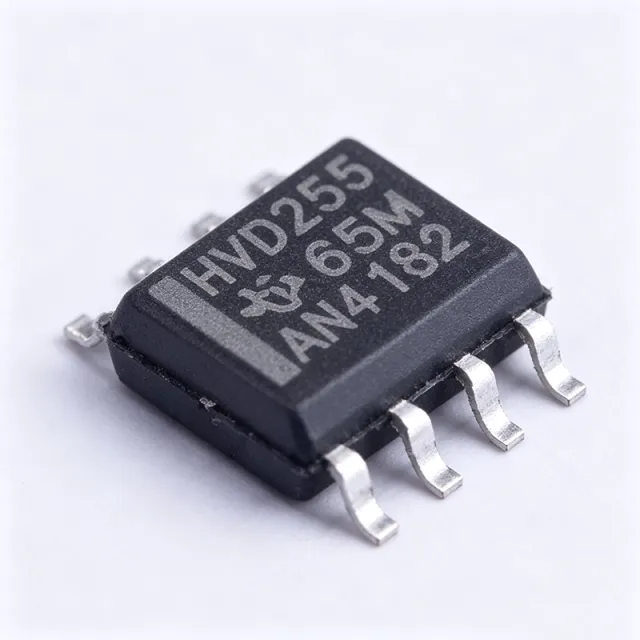
SN65HVD255DR - 1Mbps Turbo CAN Transceiver | TI
The Texas Instruments SN65HVD255DR is a Turbo CAN transceiver designed for highly loaded Controller Area Network (CAN) networks with data rates in excess of 1 Mbps. It is packaged in an 8-pin SOIC (D) surface-mount package and operates over an extended temperature range of -40C to +125C, implementing the ISO 11898-2 High-Speed CAN physical layer standard. A CAN transceiver is the physical-layer interface between a CAN protocol controller and the twisted-pair bus, converting controller TXD/RXD logic signals into differential CANH/CANL signals. Within the CAN system hierarchy (application layer, protocol controller, transceiver, bus), the transceiver provides the drive strength, common-mode tolerance, and ESD/fault robustness required for reliable communication in harsh electrical environments. Key features include fast loop propagation times that enhance timing margins on long, heavily loaded networks; functional-safety-oriented features per the TI datasheet; dominant and recessive output drive compliant with ISO 11898-2; and internal protection including thermal shutdown and short-circuit current limiting. The device operates from a nominal 5V supply. Low electromagnetic emission and high immunity make it suitable for demanding automotive and industrial buses. Typical applications include industrial automation and motor drives, building and climate control automation, security systems, and telecom base station status and control networks. In these systems the Turbo CAN fast loop times allow more nodes, longer cable runs, or higher bit rates than standard transceivers. When designing with the SN65HVD255DR, terminate both bus ends with 120-ohm resistors, place a 0.1uF bypass capacitor close to VCC, and keep the CANH/CANL traces symmetric and short to preserve signal integrity at extended data rates.

TCAN330GDR - 3.3V 5Mbps CAN FD Transceiver | Texas Instruments
The Texas Instruments TCAN330GDR is a 3.3-V single-channel CAN FD transceiver with a maximum signaling rate of 5 Mbps, designed for high-speed CAN bus communication. It is supplied in an 8-pin SOIC (D) package and supports the ISO 11898-2 high-speed CAN physical-layer standard. The device operates from a 3.0-V to 3.6-V single supply, making it suitable for embedded, industrial, and communications systems that use 3.3-V controller I/O. A CAN transceiver, also called a CAN physical-layer interface, converts logic-level signals from a CAN controller into differential bus signals and converts received differential signals back into digital logic. In the broader hierarchy, TCAN330GDR belongs to the CAN interface IC class, which sits within interface ICs and semiconductor communication components. Its CAN FD capability allows the physical layer to support higher signaling rates than classic CAN while maintaining compatibility with established CAN network infrastructure. Key features include single-supply operation from 3.0 V to 3.6 V, operation up to 5 Mbps, ISO 11898-2 compatibility, a wide common-mode operating range of ±12 V, and bus-pin fault protection to ±14 V. The TCAN330G family includes normal mode, silent mode, and shutdown mode functions, with the exact mode behavior depending on the selected family member. The TCAN330GDR uses the 8-pin SOIC package, which supports conventional surface-mount assembly and is available in standard distributor inventory. The TCAN330GDR is designed for systems in which a CAN controller or MCU includes a CAN host interface but requires an external physical-layer transceiver. Its 5-Mbps capability is useful for CAN FD nodes in industrial automation, automotive electronics, embedded control, and communication equipment. The ±14-V bus-pin fault protection provides additional robustness when the transceiver is connected to an externally powered or noisy vehicle, machine, or industrial bus. When designing a TCAN330GDR circuit, verify the controller supply level, CAN bus termination, common-mode range, and transceiver mode requirements against the complete datasheet. Place the transceiver close to the CAN connector, provide a proper ground reference, and use the recommended protection and decoupling layout. The exact pin assignments and application-specific timing values are not present in the supplied source snippets and should be confirmed from the official manufacturer datasheet before PCB release. This product page consolidates verified manufacturer and distributor information, same-package family alternatives, pricing references, and engineering design guidance. It is intended to support component selection and sourcing for TCAN330GDR rather than replace the complete Texas Instruments datasheet, which remains the authoritative source for electrical limits, timing, pinout, and application guidance.

TCAN334DCNT - 3.3V 1Mbps CAN FD Transceiver | Texas Instruments
The Texas Instruments TCAN334DCNT is a 3.3 V half-duplex CAN FD transceiver with a maximum data rate of 1 Mbps, packaged in an 8-pin SOT-23 (DCN) surface-mount package. It provides the physical-layer interface between a 3.3 V CAN controller and a CAN bus, supporting transmit, receive, standby, and bus-fault signaling functions. A CAN transceiver is an interface IC that converts logic-level controller signals into physical bus signals and converts incoming bus levels into digital data for the host controller. CAN, or Controller Area Network, is a deterministic multi-node serial-bus technology widely used in automotive, industrial, robotics, and embedded systems. CAN FD extends classical CAN by carrying larger data payloads while maintaining compatibility with the physical communication environment. The TCAN334 family operates from a 3 V to 3.6 V supply, allowing direct association with 3.3 V microcontrollers and CAN controllers. Its 1 Mbps capability supports the data rates used by many classical CAN networks. The half-duplex arrangement means the transmitter and receiver share the same bus connection, while the transceiver supplies separate digital transmit and receive paths to the controller. The device is offered in the compact DCN SOT-23 package, which supports high-density PCB placement in embedded control systems. Its operating-temperature range extends from -40°C to 125°C, making it suitable for industrial and automotive-style environments when the complete system requirements are met. The transceiver also includes power-down behavior and fault-detection functions, allowing a host controller to manage bus communication and detect abnormal bus states. Typical uses include CAN-connected sensor nodes, industrial control modules, automotive body electronics, robot controllers, and factory automation equipment. In each case, the TCAN334DCNT can interface a host CAN controller to a physical CAN bus while operating from the same 3.3 V rail as the controller. Network topology, termination, isolation, and transceiver selection still require system-level validation. For PCB design, place the transceiver and its required bypass capacitor close to the associated controller and CAN connector. Keep the CANH and CANL routing short, symmetrical, and away from sensitive analog or high-speed digital traces. Verify termination placement so that the two ends of the principal bus segments use the resistance required by the CAN network design. This page combines manufacturer product data, package details, verified cross-reference candidates, and application-oriented engineering guidance. It helps engineers compare same-footprint CAN transceiver options, identify functional differences, and plan interface layouts before requesting a quotation.

TCAN337G-Q1 - 3.3V CAN FD Transceiver | Texas Instruments
The TCAN337G-Q1 is a 3.3-V CAN transceiver with CAN FD (Flexible Data Rate) capability from Texas Instruments, designed for high-speed Controller Area Network (CAN) communication in automotive and industrial applications. It is part of the TCAN33x family, which is compatible with the ISO 11898 High Speed CAN Physical Layer standard. The device supports data rates up to 5 Mbps with CAN FD, enabling faster and more reliable data transfer in modern vehicle networks. It is available in a small SOT-23-8 package, making it ideal for space-constrained designs. A CAN transceiver is a physical layer device that interfaces between a CAN controller (such as a microcontroller with an integrated CAN peripheral) and the differential bus lines (CANH and CANL). It converts the digital signals from the controller into differential signals for transmission over the twisted-pair bus, and vice versa. The transceiver provides the necessary drive strength, receiver sensitivity, and protection features required for robust communication in harsh environments. In the system hierarchy, a CAN transceiver sits between the CAN controller (part of the MCU) and the physical bus, forming the physical layer of the CAN network. Key features of the TCAN337G-Q1 include a wide operating voltage range of 3.0V to 3.6V, low electromagnetic emission, and high immunity to electromagnetic interference. It offers a bus fault protection of ±58V, ensuring robustness against short circuits and miswiring. The device also features a silent mode for diagnostic and network management, and a dominant timeout function to prevent bus lock-up. The TCAN337G-Q1 is AEC-Q100 qualified for automotive applications, meeting the stringent reliability requirements of the automotive industry. Technically, the TCAN337G-Q1 uses a differential signaling scheme with a common-mode range of -12V to +12V, allowing it to operate in noisy environments. It has a loop delay symmetry of [DATA_NEEDED: loop delay symmetry] ns, which is critical for CAN FD operation at high data rates. The device is designed to be pin-compatible with other TCAN33x family members, such as TCAN337G and TCAN337, enabling easy design migration. It also includes a VIO pin for level shifting, allowing direct interface with 3.3V or 5V microcontrollers. Typical applications include automotive body control modules, infotainment systems, advanced driver-assistance systems (ADAS), industrial automation, and building automation. The TCAN337G-Q1 is particularly suited for applications requiring high data rates and robust communication in harsh environments. Its small SOT-23-8 package and low power consumption make it an excellent choice for space-constrained and power-sensitive designs. When designing with the TCAN337G-Q1, ensure proper termination resistors (typically 120Ω) at both ends of the CAN bus to minimize signal reflections. Also, place the transceiver close to the connector to reduce stub length and improve signal integrity. The VIO pin should be connected to the same supply voltage as the CAN controller to ensure proper logic level compatibility.
TJA1028T/3V3/10 - 3.3V LIN Transceiver with 70mA Regulator
The NXP Semiconductors TJA1028T/3V3/10 is a LIN bus transceiver with an integrated 3.3 V low-dropout voltage regulator capable of delivering up to 70 mA, housed in an 8-pin SOIC package. It combines LIN 2.0, LIN 2.1, SAE J2602, and ISO 17987-4:2016 for 12 V systems with local power delivery for compact automotive and industrial LIN nodes. A LIN transceiver is a physical-layer interface for the Local Interconnect Network, a low-cost, single-wire serial bus commonly used to connect sensors, actuators, door modules, climate controls, and other distributed automotive electronics. The TJA1028 combines that bus interface with a 3.3 V regulator, reducing the number of components required at a compact LIN slave node. The headline features are compliance with LIN 2.0, LIN 2.1, SAE J2602, and ISO 17987-4:2016, a regulated 3.3 V output rated to 70 mA, and an 8-pin SOIC package. The integrated regulator allows a peripheral device to receive local supply from the LIN system while the transceiver communicates over the same harness. The TJA1028 family is designed for compact nodes connected to 12 V LIN networks. Its integrated regulator supports the 3.3 V variant identified by the /3V3 ordering code, while the TJA1028 family also includes a 5.0 V regulator variant. This distinction is important because replacing the 3.3 V device with the 5.0 V device changes the local supply presented to attached circuitry. Typical uses include LIN-connected sensor modules, body-control submodules, automotive door and seat electronics, climate-control nodes, and industrial control modules that use LIN for inexpensive short-range networking. Compactness and local supply integration are particularly valuable when the node must fit behind a vehicle trim panel or within a sealed enclosure. When designing a TJA1028T/3V3/10 circuit, follow the NXP datasheet wiring and decoupling recommendations, preserve the transceiver's LIN bus and ground connections, and validate the regulator load transient response at the maximum 70 mA operating point. Check the package pin assignments against the selected PCB footprint before layout. This product overview consolidates the manufacturer-defined LIN compliance, integrated 3.3 V regulator capability, package information, sourcing guidance, and engineering considerations into one reference for compact LIN-node development.

TJA1124AHG/0Z - Quad LIN Transceiver | NXP Semiconductors
The NXP Semiconductors TJA1124AHG/0Z is a quad LIN transceiver with integrated pull-up resistors, packaged in a 24-terminal DHVQFN surface-mount package. It provides four LIN channels for controller-area-network communication in automotive electronics, combining LIN signal conditioning, bus termination, receive filtering, and transmit drive functions in one device. The verified manufacturer product page identifies the TJA1124AHG as an active quad LIN transceiver, while the manufacturer datasheet describes optimized LIN output waveforms and internal LIN commander termination resistors. A LIN transceiver is an interface integrated circuit that connects a microcontroller to a Local Interconnect Network bus. It converts microcontroller transmit commands into shaped LIN bus signals, receives bus states through high-impedance inputs, and transfers receive data to the host controller. LIN buses are commonly used for low-cost vehicle sub-networks involving sensors, switches, actuators, lighting, seat controls, and body electronics. The TJA1124AHG/0Z supports four independent LIN channels, reducing the number of interface devices required in a multi-node vehicle body controller. Its internal pull-up resistors help simplify bus implementation, while the LIN output stage is designed to produce low-emission bus signals. The receiver paths report bus activity to a microcontroller through dedicated receive pins, allowing the host processor to determine LIN frame status. The device is associated with an AEC-Q100 automotive qualification in distributor product information and an operating-temperature range of -40°C to 150°C junction temperature. Its 24-DHVQFN package is approximately 5.5 mm by 3.5 mm and includes an exposed thermal pad, supporting compact automotive controller layouts while providing a thermal path for the LIN output drivers. Typical applications include automotive body-domain controllers, door modules, climate-control panels, lighting controllers, seat and switch assemblies, ambient-sensing nodes, and central comfort systems. Four channels are especially useful when several distributed LIN loads share one central ECU. Designers should maintain the required external baud-rate timing, pull-up resistor, bus capacitance, and termination values from the manufacturer datasheet. This page combines the manufacturer datasheet and product-page information with pin-compatible family references, application guidance, and design checks for evaluating the TJA1124AHG/0Z in automotive LIN networks. Because the exact package pin names, electrical limits, and variant-specific behavior must be confirmed against the current NXP documentation before PCB release, use the pin-description and electrical-characteristics tables in the TJA1124 datasheet as the final engineering references.
TJA1128HTK/0Z LIN SBC with 85 mA LDO, 14-HVSON | NXP
The NXP Semiconductors TJA1128HTK/0Z is a LIN Mini System Basis Chip (SBC) that combines a half-duplex LIN transceiver, an 85 mA low-dropout voltage regulator, a window watchdog, two WAKE inputs, one general purpose input (GPI) and one high-voltage multipurpose (HVMPO) output in a 14-HVSON (3 x 4.5 mm) surface-mount package. A system basis chip sits between a microcontroller and the rest of an automotive electrical system, bundling the power conversion, bus interface and supervision functions that a node needs to talk to the vehicle network and to the outside world. In the hierarchy of automotive electronics, the TJA1128 is a LIN transceiver integrated into an SBC, which itself is a power-management and communication IC rather than a discrete transceiver. The TJA1128 also carries AEC-Q100 automotive qualification, so it is intended for harsh in-vehicle conditions rather than for consumer equipment. Key features include an integrated LDO capable of delivering up to 85 mA, available in 3.3 V and 5.0 V output versions, which removes the need for a separate regulator for small-signal sensor and logic nodes. The chip adds a window watchdog for host supervision, two wake inputs so the node can be brought out of sleep by external activity, a general purpose input for discrete switch sensing, and an HVMPO output capable of driving higher-current loads than a standard GPIO. The LIN transceiver is a 1/1 half-duplex implementation, matching the single-wire LIN physical layer. Architecturally, the device splits its supply into a battery-connected high-voltage domain for the LIN bus and wake detection and a regulated domain for the logic and microcontroller interface. That split lets the node remain operable while the host microcontroller is held in reset or power-down, which is the basis of the very low power operating modes described in the NXP TJA1128 datasheet. Typical applications include LIN sub-networks in body control modules, seat and door modules, smart junction boxes, ambient lighting controllers, LIN sensor nodes such as seat-occupancy or ambient sensors, and compact battery-backed telematics units where a single component must handle bus communication, regulation and host supervision. When designing around this part, budget the LDO current carefully: the 85 mA rating covers the transceiver, the local microcontroller and attached sensors, but not motors or lamps. Confirm headroom for the host supply so the regulator does not enter thermal or current limiting during load transients, and review the window-watcher timing in the datasheet against your host refresh cycle. This page brings together the manufacturer datasheet detail, package and pin information, drop-in alternatives and practical design notes so that an engineer can qualify the TJA1128HTK/0Z for a LIN node without chasing several documents.
TJA1441ATK/0Z - 5 Mbps CAN FD Transceiver | NXP
NXP Semiconductors TJA1441ATK/0Z is a high-speed CAN transceiver with Silent mode, one transmitter, and one receiver for Classical CAN and CAN FD networks. It operates from a 4.5 V to 5.5 V supply, supports data rates up to 5 Mbps, and is supplied in an 8-HVSON surface-mount package with a nominal body size of 3 mm by 3 mm. The device is listed as active and its series is identified as automotive and AEC-Q100. A CAN transceiver, also called a CAN bus interface or CAN controller interface, is the physical-layer component that connects a host controller or microcontroller to a differential CAN network. It converts logic-level signaling into the differential bus waveform and receives bus information back as digital logic. The TJA1441 family combines a CAN transmitter and receiver in one package, reducing component count while preserving compatibility with established CAN hardware. The principal benefits of the TJA1441ATK/0Z are its support for CAN FD, its 5 Mbps maximum data rate, and its Silent mode. Silent mode allows the transmitter to be disabled while the receiver continues monitoring bus activity, which is useful in power-management and bus-management arrangements. NXP describes the family as a straightforward replacement for high-speed Classical CAN and CAN FD transceivers such as the TJA1051 and TJA1057, with pin compatibility intended to reduce hardware and software changes during retrofit work. The TJA1441ATK/0Z is a half-duplex interface with one transmitter and one receiver. Its 8-HVSON package is intended for surface-mount assembly and tape-and-reel production. The specified operating range extends from -40 °C to 150 °C junction temperature, supporting industrial and automotive environments where temperature, EMI behavior, and dependable bus operation are important. Typical uses include automotive body and comfort electronics, industrial automation equipment, embedded control systems, CAN-based diagnostics, and retrofit platforms that previously used compatible NXP transceivers. The small 3 mm by 3 mm package also helps reduce board area beside tightly spaced microcontrollers, transceivers, and power-management components. When laying out the device, follow the manufacturer datasheet for CANH, CANL, VCC, ground, mode-control, RXD, and exposed-pad connections. Preserve the recommended termination and common-mode network implementation, and keep high-current bus paths compact. Validate silent-mode polarity and external transceiver logic against the host firmware before using the part for wake-up or redundant-bus arrangements. This product page combines the manufacturer specification with practical guidance for package selection, CAN bus integration, thermal and PCB considerations, qualification status, and drop-in replacement evaluation. It is intended to help engineers compare the TJA1441ATK/0Z against established NXP CAN interfaces before committing a board revision.
TJA1441DT/0Z - 5 Mbit/s CAN FD Transceiver | NXP
The NXP Semiconductors TJA1441DT/0Z is a high-speed CAN and CAN FD transceiver designed for use between a CAN protocol controller and a two-wire CAN bus. It supports CAN FD communication at data rates up to 5 Mbit/s and is presented in an 8-pin SO package. The device is intended as a replacement for high-speed Classical CAN and CAN FD transceivers, including NXP TJA1051 and TJA1057 devices, while preserving existing hardware and software designs. The TJA1441 belongs to the NXP TJA144x family of CAN transceivers. This family provides the physical-layer interface between a CAN controller and the differential CAN bus, allowing a host processor or dedicated CAN controller to exchange frames with other nodes. The family includes single-channel devices such as the TJA1441, TJA1442 and TJA1443, as well as the dual-channel TJA1448. Supporting CAN FD enables the transceiver to participate in networks carrying larger payloads and higher data rates than Classical CAN. The TJA1441DT/0Z includes selectable operating behavior described in the manufacturer documentation as Silent mode and selectable Off mode. These functions are useful in automotive and industrial CAN networks where a node may need to reduce bus activity, enter a low-power state, or control when its transmitter is connected to the bus. The transceiver also supports fault-tolerant CAN bus operation, an important characteristic for systems exposed to wiring faults, shorts, or excessive bus loading. Typical applications include electronic control units, body and chassis controllers, gateway modules, instrumentation, industrial automation equipment, diagnostic tools and CAN FD gateways. In these systems, the transceiver translates the controller's TXD logic signal into the differential CANH and CANL bus levels and converts received bus activity into an RXD signal for the controller. For PCB layout, place the transceiver close to the CAN connector or bus-header interface and keep the CANH and CANL routing symmetrical. Provide a solid ground-plane connection and follow the decoupling recommendations in the manufacturer datasheet. The bus network must also satisfy the termination, cable-length and topology requirements for the selected CAN communication standard. This product page combines the NXP family description, verified distributor identifiers, package information, replacement guidance and application-specific design considerations. It also provides drop-in alternatives identified from the available cross-reference information, allowing engineers to compare same-package candidates before changing an existing design.