STM32H730VBT6
STM32H730VBT6 - 550MHz Cortex-M7 MCU with 128KB RAM | STMicroelectronics
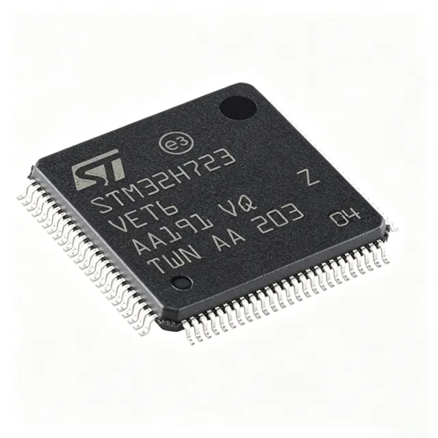
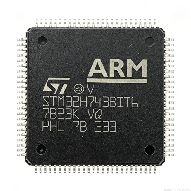
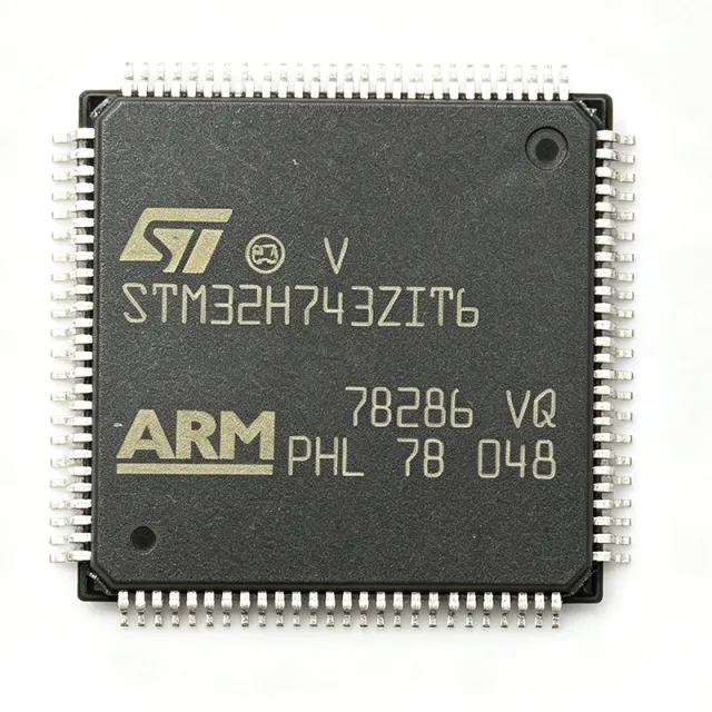
The STMicroelectronics STM32H730VBT6 is a high-performance 32-bit microcontroller based on the Arm Cortex-M7 core, operating at up to 550 MHz. It is part of the STM32H7 series, designed for applications requiring intensive computation, advanced connectivity, and rich peripheral integration. The device comes in a 100-pin LQFP package (LQFP100) and offers 128 KB of SRAM and 128 KB of flash memory, with an extensive set of peripherals including multiple communication interfaces, timers, ADCs, DACs, and cryptographic acceleration.
What is a microcontroller? A microcontroller (MCU) is a compact integrated circuit designed to govern a specific operation in an embedded system. It contains a processor core, memory (RAM and flash), and programmable input/output peripherals on a single chip. Microcontrollers are the brain of countless electronic devices, from automotive engine control units to IoT sensors and industrial automation systems. In the hierarchy of computing devices, a microcontroller sits between a simple logic gate and a full application processor, offering a balance of performance, power efficiency, and cost for dedicated control tasks.
Key features of the STM32H730VBT6 include a 550 MHz Arm Cortex-M7 core with double-precision floating-point unit (FPU), 128 KB of SRAM, and 128 KB of flash memory. It supports a wide range of communication interfaces: 6x SPI, 4x I2C, 4x USART, 2x UART, 2x FDCAN, 2x SDMMC, 1x USB 2.0 OTG FS/HS, 1x Ethernet MAC, and 1x camera interface. The device also integrates a 16-bit ADC with 3.6 MSPS, a 12-bit DAC, multiple 16-bit and 32-bit timers, and a true random number generator (TRNG). For security, it includes hardware cryptographic acceleration (AES, DES, 3DES, SHA-1, SHA-256, and CRC).
The STM32H730VBT6 is built on a high-performance architecture with an L1 cache (I-Cache and D-Cache) to optimize execution from external memory. It supports external memory interfaces for SDRAM, SRAM, and NOR/NAND flash via FMC (Flexible Memory Controller). The device operates from a 1.62V to 3.6V power supply and features multiple low-power modes (Sleep, Stop, Standby) to optimize energy consumption. The LQFP100 package provides a compact footprint with 100 pins, including multiple GPIOs with alternate functions.
Typical applications include industrial control systems, motor control, advanced IoT gateways, audio processing, and high-end consumer electronics. The combination of high clock speed, rich peripherals, and security features makes it suitable for real-time control and edge computing tasks. For example, in motor control, the high-resolution timers and ADC enable precise field-oriented control (FOC) of brushless DC motors.
When designing with this device, ensure proper decoupling of the power supply pins with 100nF capacitors close to each VDD pin and a bulk capacitor (e.g., 4.7uF) at the main supply. The VDDA pin must be connected to a clean analog supply, and VREF+ should be decoupled with a 1uF capacitor. For high-speed interfaces like USB and Ethernet, follow the layout guidelines in the datasheet to maintain signal integrity.
USD $8,10
Auf Lager