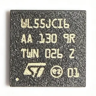
ADRV9009BBCZ - Dual RF Transceiver 75MHz-6GHz | Analog Devices
Teilenummer: ADRV9009BBCZ ✓ Aktiv| Menge | Stückpreis | Gesamt |
|---|---|---|
| 1 | $245 | $245,00 |
| 10 | $220.5 | $2.205,00 |
| 100 | $196 | $19.600,00 |
| 500 | $171.5 | $85.750,00 |
| 1.000 | $147 | $147.000,00 |
ADRV9009BBCZ Übersicht
An RF transceiver is a device that combines both a transmitter and a receiver in a single package, enabling bidirectional communication over radio frequencies. The ADRV9009 is a key component in modern wireless systems, providing the analog and digital signal processing needed to convert between baseband data and RF signals. It integrates multiple functions such as filtering, amplification, and frequency synthesis, reducing the need for external components and simplifying system design.
Key features of the ADRV9009BBCZ include support for 3G, 4G, and 5G macro cell time division duplex (TDD) base station applications, dual transmitters and receivers, and an observation receiver for transmit monitoring. The device also includes integrated synthesizers and digital signal processing, enabling high performance with low power consumption. The operating temperature range is -40°C to +85°C, and the device is RoHS compliant.
The ADRV9009 utilizes advanced mixed-signal processing to achieve high dynamic range and low noise, essential for demanding cellular infrastructure applications. Its agile frequency synthesis allows rapid hopping across the 75 MHz to 6 GHz band, supporting multi-band and multi-standard radios. The integrated digital signal processing offloads the baseband processor, reducing system complexity and power consumption.
Typical applications include 3G/4G/5G macro cell base stations, small cells, and other wireless infrastructure. The device is also used in phased array radar, satellite communications, and test and measurement equipment. Its wide frequency range and high integration make it a versatile choice for many RF systems.
When designing with the ADRV9009, careful attention must be paid to power supply decoupling and thermal management. The device requires multiple supply rails (1.3V, 1.8V, 1.89V) and a well-designed PCB layout to achieve optimal performance. Reference designs and evaluation boards are available from Analog Devices to accelerate development.
Drop-in-Alternativen für ADRV9009BBCZ – gleiches Gehäuse, Pin-kompatibel. Bauteile mit anderem Gehäuse, die eine PCB-Überarbeitung erfordern, sind ausgeschlossen.
Varianten dieser Serie
Modelle derselben Serie, die drop-in-kompatibel sind mit ADRV9009BBCZ (gleiche Bauform und Footprint) – abweichend in Frequency Range, Package, Supply Voltage, Number of Transmitters, Type.
Schnellvergleichstool – Wählen Sie Alternativbauteile für den Direktvergleich:
ADRV9009BBCZ-REEL
✅ Drop-In✓ Auf Lager
$300 / Stück
Datenblatt ansehen →ADRV9004BBCZ
✅ Drop-In ⚠️ Spezifikationen ungeprüft✓ Auf Lager
$90 / Stück
Datenblatt ansehen →ADRV9003BBCZ
✅ Drop-In ⚠️ Spezifikationen ungeprüft✓ Auf Lager
$95 / Stück
Datenblatt ansehen →ADRV9002BBCZ
✅ Drop-In ⚠️ Spezifikationen ungeprüft✓ Auf Lager
$210 / Stück
Datenblatt ansehen →AD9361BBCZ
✅ Drop-In ⚠️ Spezifikationen ungeprüft✓ Auf Lager
$62 / Stück
Datenblatt ansehen →ADRV9009BBCZ Technische Daten
| Frequency Range | 75 MHz to 6 GHz |
| Number of Transmitters | 2 |
| Number of Receivers | 2 |
| Observation Receiver | 1 |
| Versorgungsspannung | 1.3V, 1.8V, 1.89V |
| Gehäuse | 196-pin CSP-BGA |
| Montageart | Surface Mount |
| Betriebstemperaturbereich | -40°C to +85°C |
| RoHS | Compliant |
| Schnittstelle | JESD204B |
| Applications | 3G/4G/5G TDD Base Stations |
| Integrated Synthesizers | Yes |
| Digital Signal Processing | Yes |
ADRV9009BBCZ Pin-Konfiguration
| Pin A1 | GND — Ground |
| Pin A2 | VDD_1P3 — 1.3V power supply |
| Pin A3 | VDD_1P8 — 1.8V power supply |
| Pin A4 | VDD_1P89 — 1.89V power supply |
| Pin B1 | TX1_P — Transmitter 1 positive output |
| Pin B2 | TX1_N — Transmitter 1 negative output |
| Pin C1 | TX2_P — Transmitter 2 positive output |
| Pin C2 | TX2_N — Transmitter 2 negative output |
| Pin D1 | RX1_P — Receiver 1 positive input |
| Pin D2 | RX1_N — Receiver 1 negative input |
| Pin E1 | RX2_P — Receiver 2 positive input |
| Pin E2 | RX2_N — Receiver 2 negative input |
| Pin F1 | ORX_P — Observation receiver positive input |
| Pin F2 | ORX_N — Observation receiver negative input |
| Pin G1 | CLK_P — Clock positive input |
| Pin G2 | CLK_N — Clock negative input |
Typische Anwendungen
ADRV9009BBCZ ist geeignet für 6 Anwendungs: 5G Macro Cell Base Stations, Small Cells, Phased Array Radar, Satellite Communications, Test and Measurement Equipment, Wireless Infrastructure.
5G Macro Cell Base Stations
The ADRV9009BBCZ is designed for 3G/4G/5G macro cell TDD base stations. Its dual transmitters and receivers enable multiple channels, while the integrated synthesizers and DSP reduce external components. The wide frequency range (75MHz-6GHz) supports various bands, and the observation receiver allows transmit monitoring for linearization.
Empfohlen
Small Cells
For small cell deployments, the ADRV9009BBCZ provides a compact, high-integration solution. Its low power consumption and small footprint (196-pin CSP-BGA) are ideal for space-constrained enclosures. The device supports multiple frequency bands, enabling multi-standard operation in a single design.
Empfohlen
Phased Array Radar
The ADRV9009BBCZ's agile frequency synthesis and wide bandwidth make it suitable for phased array radar systems. Its dual transmitters and receivers support multiple channels, while the integrated DSP enables beamforming algorithms. The observation receiver aids in calibration and monitoring.
Empfohlen
Satellite Communications
In satellite communications, the ADRV9009BBCZ provides reliable RF performance across a wide frequency range. Its high integration reduces board space and power consumption, critical for space-constrained payloads. The device supports various modulation schemes and can be configured for different satellite bands.
Empfohlen
Test and Measurement Equipment
The ADRV9009BBCZ is used in test and measurement equipment such as spectrum analyzers and signal generators. Its wide frequency range and high dynamic range enable accurate signal analysis. The integrated synthesizers allow precise frequency tuning, and the dual channels support MIMO testing.
Empfohlen
Wireless Infrastructure
The ADRV9009BBCZ is a versatile choice for various wireless infrastructure applications, including repeaters and distributed antenna systems. Its dual transmitters and receivers enable simultaneous uplink and downlink processing. The device's wide frequency range supports multiple bands, reducing the need for multiple transceivers.
Empfohlen
Zusammenfassung der empfohlenen Produkte
Technische Referenzdaten für ADRV9009BBCZ – Vergleich, Designhinweise und Compliance-Informationen.
Auswahlhilfe
Vergleich mit Alternativen
| Parameter | Dieses Produkt | ADRV9009BBCZ-REEL | ADRV9004BBCZ | ADRV9003BBCZ | ADRV9002BBCZ | AD9361BBCZ |
|---|---|---|---|---|---|---|
| Package | 196-pin CSP-BGA | 196-pin CSP-BGA | 196-pin CSP-BGA | 196-pin CSP-BGA | 196-pin CSP-BGA | 196-pin CSP-BGA |
| Brand | Analog Devices | Analog Devices | Analog Devices | Analog Devices | Analog Devices | Analog Devices |
| Frequency Range | 75 MHz to 6 GHz | 75 MHz to 6 GHz | 75 MHz to 6 GHz | 75 MHz to 6 GHz | 75 MHz to 6 GHz | 70 MHz to 6 GHz |
| Number of Transmitters | 2 | 2 | 1 | 1 | 1 | 2 |
| Number of Receivers | 2 | 2 | 1 | 1 | 1 | 2 |
| Observation Receiver | Yes | Yes | No | No | No | Yes |
| Supply Voltage | 1.3V, 1.8V, 1.89V | 1.3V, 1.8V, 1.89V | 1.3V, 1.8V, 1.89V | 1.3V, 1.8V, 1.89V | 1.3V, 1.8V, 1.89V | 1.3V, 1.8V, 2.5V |
| Operating Temperature | -40°C to +85°C | -40°C to +85°C | -40°C to +85°C | -40°C to +85°C | -40°C to +85°C | -40°C to +85°C |
Wichtigste Unterscheidungsmerkmale
- Dual transmitters and receivers with observation receiver (vs. ADRV9004BBCZ)
- Wide frequency range up to 6 GHz (vs. AD9361BBCZ)
- Integrated observation receiver (vs. ADRV9002BBCZ)
Designhinweise
The ADRV9009BBCZ requires multiple supply rails: 1.3V, 1.8V, and 1.89V. Use low-noise LDOs or switching regulators with proper filtering to ensure clean power. Decouple each supply pin with 100nF and 10uF capacitors placed close to the pins. Refer to the Analog Devices reference design for recommended power tree.
The device dissipates significant power, especially in transmit mode. Ensure adequate thermal management by using a thermal pad and vias to a ground plane. The 196-pin CSP-BGA package has an exposed pad that must be soldered to the PCB for heat dissipation. Consider forced air cooling for high-power applications.
For optimal RF performance, use controlled impedance traces for RF inputs and outputs. Keep RF traces short and avoid sharp bends. Use a solid ground plane beneath the device and provide adequate grounding for the CSP-BGA package. Follow the layout guidelines in the ADRV9009 datasheet and evaluation board design files.
Compliance-Informationen
RoHS compliant per distributor data. Other compliance information not specified in the provided data.