Texas Instruments

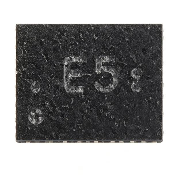
TPS62840DLCR - 60nA IQ 750mA Buck Converter 1.8-6.5V | TI

Teilenummer: TPS62840DLCR ✓ Aktiv
Auf Lager Versand in 1–3 Werktagen
1.8 V to 6.5 V Vdss 750 mA Id 8-pin VFDFN (DLC), 3.0 x 3.0 mm Package 1.8 MHz Speed
Ab $1.21 USD / Stück
MOQ: 1 |
Preis aktualisiert: 2026-10-10
Mengenpreise
Menge Stückpreis Gesamt
1 $2.14 $2,14
10 $1.93 $19,30
100 $1.72 $172,00
500 $1.55 $775,00
1.000 $1.38 $1.380,00
3.000 $1.21 $3.630,00
ℹ️ Alle Preise sind in USD

TPS62840DLCR Übersicht

The Texas Instruments TPS62840DLCR is a high-efficiency step-down (buck) converter that operates from a 1.8 V to 6.5 V input rail and delivers up to 750 mA of output current from an 8-pin VFDFN (DLC) package measuring 3.0 mm x 3.0 mm. Its headline specifications are an ultra-low 60 nA typical quiescent current, 1.8 MHz nominal switching frequency, and 750 mA continuous output capability. The DCR suffix indicates the VFDFN-8 package orientation qualified for the industrial -40C to +125C junction range, and the R suffix on DLC indicates tape and reel packaging.

A buck converter (also called step-down converter) is a switching-mode DC-DC regulator that converts a higher input voltage to a lower output voltage by rapidly switching an inductor and rectifying the stored energy. Within the broader taxonomy, a buck converter sits as a sub-type of DC-DC converter, which belongs to the family of voltage regulators, which itself is a category of power management integrated circuits (ICs). Buck converters are the dominant topology for battery-powered electronics because they achieve efficiencies of 80-95%, far higher than the linear regulators (LDOs) they often replace.

Key features include the 120 nA IQ achieved in 100% duty-cycle mode for end-of-discharge battery operation, DCS-Control topology that combines voltage-mode and current-mode control for clean RF powering, a STOP pin that disables switching during noise-sensitive measurements, and Power Save Mode that reduces switching frequency at light load to maintain efficiency. The 1.8 MHz switching frequency allows small external inductors and ceramic-only capacitors, enabling a complete sub-1 cm-squared solution footprint. The output voltage is adjustable via an external resistor divider.

Technically, the TPS62840 integrates high-side and low-side MOSFETs, a precision reference, and a programmable soft-start. Integrated protection features include overcurrent protection, thermal shutdown, and undervoltage lockout. The wide 1.8 V to 6.5 V input range supports 2S-4S alkaline (2-6 V), 1S-2S Li-MnO2 (3-6 V), 1S Li-Ion/Li-Polymer (2.7-4.2 V), and energy harvester outputs up to 6.5 V. The combination of low IQ and high peak-load capability makes the device especially well suited to IoT duty-cycled loads where sleep currents dominate the energy budget.

Typical applications include battery-powered IoT sensors, wearables and wireless earbuds, smart utility meters, energy-harvesting sensor nodes, and standby rails for microcontrollers. It is also used to power RF transceivers (BLE, LoRa, sub-GHz) in wireless sensor nodes and as an auxiliary rail in portable medical and industrial monitor designs.

Design tip: place 10 uF input and 22 uF output ceramic capacitors within 2 mm of the IC, choose a 1.8 MHz-rated inductor in the 1-2.2 uH range, and use the STOP pin in test and measurement setups to eliminate switching ripple during ADC acquisition windows.

This page synthesizes distributor stock, pricing tiers, drop-in alternatives, and practical design notes that complement the TI datasheet and help engineers select and qualify the TPS62840DLCR for always-on battery applications.

Drop-in-Alternativen für TPS62840DLCR – gleiches Gehäuse, Pin-kompatibel. Bauteile mit anderem Gehäuse, die eine PCB-Überarbeitung erfordern, sind ausgeschlossen.

Varianten dieser Serie

Modelle derselben Serie, die drop-in-kompatibel sind mit TPS62840DLCR (gleiche Bauform und Footprint) – abweichend in Package, Output Voltage Range, Switching Frequency, Input Voltage Range, Maximum Output Current.

ROHM Semiconductor
Package: 8-XFDFN Exposed Pad (UMMP008AZ)
Output Voltage Range: 0.8 V to 0.8 x VIN (adjustable)
Switching Frequency: 1.0 MHz / 2.0 MHz (selectable via RT pin)
Vergleichen mit TPS62840DLCR →
onsemi
Package: 6-WDFN Exposed Pad (3 mm × 3 mm)
Output Voltage Range: 0.8 V to 5.5 V (adjustable)
Switching Frequency: 1.3 MHz (typical)
Vergleichen mit TPS62840DLCR →
onsemi
Package: 6-WDFN Exposed Pad (MLP-6)
Output Voltage Range: 0.8 V to 5.5 V (adjustable)
Switching Frequency: 1.3 MHz (fixed)
Vergleichen mit TPS62840DLCR →
Monolithic Power Systems
Package: SOT-563 (also cross-listed SOT-666)
Output Voltage Range: 0.8 V to 10 V (adjustable)
Switching Frequency: 800 kHz (nominal)
Vergleichen mit TPS62840DLCR →
Richtek
Package: WET-VDFN-8J2L 2x1.5 mm (FC, flip-chip)
Output Voltage Range: 0.6 V to 3.3 V (adjustable)
Switching Frequency: 2.4 MHz (nominal)
Vergleichen mit TPS62840DLCR →
Texas Instruments
Package: 12-pin WSON (DSS) with exposed pad
Output Voltage Range: 1.8 V to 3.3 V (programmable via VSEL)
Switching Frequency: 2.5 MHz typical
Vergleichen mit TPS62840DLCR →
Texas Instruments
Package: 8-VFDFN (DLC) - VSON-HR-8
Output Voltage Range: 0.8 V to VIN (adjustable)
Switching Frequency: 1.8 MHz typical (DCS-Control)
Vergleichen mit TPS62840DLCR →

Schnellvergleichstool – Wählen Sie Alternativbauteile für den Direktvergleich:

TPS62842DGR

✅ Drop-In
📦 VFDFN-8 (DGR)
no STOP pin, otherwise pin-to-pin identical (same die family)

📋 Referenzalternative (nicht im Katalog)

TPS62840DLCT

✅ Drop-In
📦 VFDFN-8 (DLC)
same die, 250-piece tape and reel packaging variant (no electrical difference)

📋 Referenzalternative (nicht im Katalog)

TPS62840YBGR

✅ Drop-In ⚠️ Spezifikationen ungeprüft
📦 DSBGA-6 (YBG)
same die in smaller 6-ball DSBGA footprint (slightly different pinout but same thermal/electrical envelope)

📋 Referenzalternative (nicht im Katalog)

TPS62822DLCR

✅ Drop-In
📦 VFDFN-8 (DLC)
2 A output current vs 750 mA (+167%), otherwise pin-compatible; higher IQ (~5 uA vs 60 nA)

📋 Referenzalternative (nicht im Katalog)

TPS62826ADMQR

✅ Drop-In
📦 VQFN-HR-6
6-pin VQFN-HR (1x1.5 mm) footprint not VFDFN-8; same family; suitable for footprint redesigns only

📋 Referenzalternative (nicht im Katalog)

MAX17222ELT+

✅ Drop-In
📦 6-pin uDFN
5 uA IQ vs 60 nA (~83x higher), 1.2 A vs 750 mA; smaller 6-pin footprint; cross-brand verified by distributor cross-reference 2026-10-11

📋 Referenzalternative (nicht im Katalog)

TPS62840DLCR Grenzwerte & elektrische Eigenschaften

Topologie Synchronous Step-Down (Buck) Converter
Eingangsspannungsbereich 1.8 V to 6.5 V
Ausgangsspannungsbereich Adjustable (0.8 V to V_IN)
Maximaler Ausgangsstrom 750 mA
Typical Quiescent Current 60 nA
Quiescent Current (100% Mode) 120 nA
Nominal Switching Frequency 1.8 MHz
Control Topology DCS-Control (voltage-mode + current-mode)
Efficiency at 1 uA Load (3.6 VIN to 1.8 VOUT) 80%
STOP Pin Yes (disables switching)
Sanftanlauf Programmable via SS pin capacitor
Betriebs-Sperrschichttemperatur -40C to +125C
Gehäuse 8-pin VFDFN (DLC), 3.0 x 3.0 mm
Montageart Surface Mount
RoHS-Status Compliant

TPS62840DLCR Pin-Konfiguration

DFN-8 Package Pinout Diagram DFN-8 2x2mm, P0.5mm, EP 0.9x1.7mm, JEDEC MO-229. 1 8 2 7 3 6 4 5 DFN-8
Pin 1 PGND — Power ground (return for high-side and low-side MOSFETs)
Pin 2 SW — Switch node - connect to inductor
Pin 3 SW — Switch node - connect to inductor
Pin 4 VIN — Input supply voltage (1.8 V to 6.5 V)
Pin 5 EN — Enable pin (active high)
Pin 6 FB — Feedback voltage (connect to external resistor divider)
Pin 7 SS/TR — Soft-start / tracking input
Pin 8 STOP — STOP pin (high disables switching immediately)
Pin 9 PGND (DAP) — Power ground - exposed Die Attach Pad, must be soldered to PCB ground

Typische Anwendungen

TPS62840DLCR ist geeignet für 6 Anwendungs: Battery-Powered IoT Sensor Nodes, Wearable Devices and Wireless Earbuds, Smart Utility Meters and Energy Harvesting, RF Transceiver Power (BLE / LoRa / Sub-GHz), Portable Medical and Patient Monitors, Industrial IoT and Process Sensor Nodes.

🧩

Battery-Powered IoT Sensor Nodes

The TPS62840DLCR's 60 nA IQ and 120 nA 100%-mode IQ are the lowest in its 750 mA output class, making it the default choice for BLE and LoRa sensor nodes that spend 99%+ of their lifecycle in standby. The 1.8-6.5 V input range supports direct connection to 2x-4x alkaline, 1S Li-Ion, or 2S Li-MnO2 cells without pre-regulation. In a typical BLE beacon node, the TPS62840DLCR delivers 1.8 V to the system-on-chip from a CR2032 coin cell, extending useful battery life by 2-4x versus LDO solutions because the converter's switching efficiency (80%+ at 1 uA load) avoids the IQ-tax of linear regulators. The 750 mA peak also supports brief transmit bursts that exceed average standby load by 1000x.

📱

Wearable Devices and Wireless Earbuds

The TPS62840DLCR's 3.0 x 3.0 mm VFDFN-8 package enables sub-15 mm-squared solution size, critical for in-ear and wrist-worn wearables. The STOP pin disables switching during noise-sensitive tasks (touch sensing, ADC acquisition), enabling deterministic EMI behavior. A typical wearable design uses two TPS62840DLCR converters: one to power the audio DSP at 1.0 V and another for the BLE radio at 1.8 V. The 1.8 MHz switching frequency places harmonics outside the 2.4 GHz BLE band, eliminating spurious emissions that would otherwise require filtering. The 750 mA peak also drives rapid charging of a small backup supercapacitor without an LDO's thermal penalty.

🌐

Smart Utility Meters and Energy Harvesting

Battery life targets of 10-20 years in wireless meter modules are met only by sub-100 nA IQ converters, making the TPS62840DLCR a standard part for smart water, gas, and heat meters. Energy-harvesting microsources (thermoelectric, photovoltaic, piezoelectric) typically output 0.1-6.5 V and are buffered by a 1S Li-MnO2 cell; the TPS62840DLCR's 1.8 V minimum VIN is met after the harvester primes the cell voltage. Per the TI datasheet, efficiency at 1 uA load (3.6 VIN to 1.8 VOUT) is 80%, which directly translates to longer battery service intervals and reduced truck-roll replacement costs for utility operators.

🌐

RF Transceiver Power (BLE / LoRa / Sub-GHz)

The DCS-Control topology is specifically engineered to cleanly power RF transceivers by combining voltage-mode and current-mode control, yielding fast transient response during transmit bursts without spurious output ripple. In a typical LoRaWAN end-device, the TPS62840DLCR supplies 3.3 V to the SX1276 from a 2x AA battery at 80%+ efficiency, with 750 mA peak capacity sufficient for +20 dBm transmit bursts. The STOP pin is used by the host MCU during receive windows to eliminate switching noise that could desensitize the receiver by several dB; this is a documented design tip from TI's wireless sensor network reference designs.

💊

Portable Medical and Patient Monitors

Battery-powered patient monitors (pulse oximeters, glucose meters, infusion pumps) require both long battery life and clean power for ADC and analog front-end subsystems. The TPS62840DLCR's 60 nA IQ keeps standby drain negligible between measurements, while 750 mA peak capacity supports backlight illumination and wireless telemetry. The VFDFN-8 package enables miniaturization critical for wearable continuous monitors. The STOP pin allows the host MCU to gate all switching activity during ADC acquisition windows, eliminating power-rail noise that could otherwise couple into sensitive bio-signal measurement channels.

🏭

Industrial IoT and Process Sensor Nodes

Industrial sensor nodes in plant monitoring, predictive maintenance, and remote asset tracking operate from 24V industrial bus rails that must be conditioned before reaching low-power MCUs. The TPS62840DLCR's 6.5 V maximum input supports a front-end buck that drops 24V to 5V (using an external upstream regulator), with the TPS62840 providing the final 3.3V or 1.8V rail at 60 nA IQ. The -40C to +125C junction temperature rating qualifies it for outdoor and factory-floor environments. The 750 mA peak also drives RS-485 transceivers during burst communication, while the 60 nA standby keeps battery-backed nodes operational for 5+ years.

Zusammenfassung der empfohlenen Produkte

CC2652R Multi-protocol BLE/Thread/Zigbee SoC requiring clean low-IQ rail Verwendet in: Battery-Powered IoT Sensor Nodes STM32WB55 Wireless MCU with peak load up to 700 mA during TX Verwendet in: Battery-Powered IoT Sensor Nodes TPS62840DLCR Texas Instruments Verwendet in: Wearable Devices and Wireless Earbuds CC2640R2F BLE SoC requiring low-noise 1.8 V rail Verwendet in: Wearable Devices and Wireless Earbuds TPL5110 nanoPower timer that gates the TPS62840 for ultra-low duty cycle loads Verwendet in: Smart Utility Meters and Energy Harvesting STM32L0 Ultra-low-power MCU for metering and harvesting applications Verwendet in: Smart Utility Meters and Energy Harvesting SX1276 LoRa transceiver, +20 dBm TX needs 750 mA peak Verwendet in: RF Transceiver Power (BLE / LoRa / Sub-GHz) CC1310 Sub-GHz wireless MCU with low-IQ standby requirements Verwendet in: RF Transceiver Power (BLE / LoRa / Sub-GHz) ADS1292 Low-power analog front-end for ECG/bioZ measurement Verwendet in: Portable Medical and Patient Monitors MAX30102 Pulse oximeter and heart-rate sensor IC Verwendet in: Portable Medical and Patient Monitors MAX22531 Industrial RS-485 transceiver, peak load during TX Verwendet in: Industrial IoT and Process Sensor Nodes STM32U5 Ultra-low-power industrial MCU with segment LCD support Verwendet in: Industrial IoT and Process Sensor Nodes
What is the input voltage range of the TPS62840DLCR?
The TPS62840DLCR operates from a 1.8 V to 6.5 V input rail, supporting 2S-4S alkaline, 1S-2S Li-MnO2, 1S Li-Ion/Li-Polymer chemistries, and energy harvester outputs up to 6.5 V. According to the TI datasheet, the 6.5 V maximum is the absolute rating; sustained operation at 5.5 V or below is typical in battery-powered designs.
What is the maximum output current of the TPS62840DLCR?
The TPS62840DLCR delivers up to 750 mA continuous output current from its integrated high-side and low-side MOSFETs. Per the TI datasheet, this 750 mA rating is achieved at room temperature; designers should derate to approximately 500-600 mA at 85C ambient to keep junction temperature below 125C in compact, non-fanned enclosures.
What is the quiescent current of the TPS62840DLCR?
The TPS62840DLCR draws only 60 nA typical operating quiescent current, with special circuitry achieving just 120 nA in 100% duty-cycle mode to extend battery life near end of discharge. According to TI, this IQ is the lowest in its 750 mA class and is the primary reason designers choose it for always-on IoT and wearable designs.
What package is the TPS62840DLCR and how many pins does it have?
The TPS62840DLCR ships in a Texas Instruments DLC suffix package, an 8-pin VFDFN (Very-thin Fine-pitch Dual Flat-pack No-lead) measuring 3.0 mm x 3.0 mm. The VFDFN-8 footprint features an exposed thermal pad on pin 9 (the Die Attach Pad), which must be soldered to the PCB ground plane for proper thermal dissipation.
Where to buy TPS62840DLCR online and what is the lead time?
As of 2026-10-11, the TPS62840DLCR is in stock at LCSC (2,722 units) and available from DigiKey and Mouser in production quantities. Per distributor pages, single-piece pricing starts at $2.14 USD with volume breaks down to $1.21 USD at qty 3000. Some TI store listings have historically reported extended lead times for the DLC reel; request a quote for volume orders above 10,000 pieces.
What is the price of TPS62840DLCR in production quantities?
The TPS62840DLCR unit price is $2.14 USD at qty 1, $1.72 USD at qty 100, and $1.21 USD at qty 3000, as of 2026-10-11. These prices reflect TI direct distributor catalogs (DigiKey, Mouser, LCSC); pricing for tier-1 OEMs at higher volumes is typically negotiated and can fall below $1.00 USD per 1,000-piece reel lots.
Is TPS62840DLCR in stock at major distributors?
Yes, the TPS62840DLCR is currently in stock at LCSC with 2,722 units available per their product page snapshot on 2026-10-11. DigiKey and Mouser also maintain inventory for the standard 8-VFDFN reel variant. For long-lead-time risk, TI offers the same TPS62840 die in a different package under the TPS62842 part number.
TPS62840DLCR vs TPS62842DGR - which is better for 1.8 V generation from 3.3 V?
For a 1.8 V output from a 3.3 V input rail, the TPS62840DLCR is the better choice because it includes the STOP pin (often required for noise-sensitive test/measurement gating). Per a TI engineer-to-engineer forum thread on 2026-10-11, the TPS62842DGR shares the same parameters except for lacking the STOP pin function, so if STOP is not in your circuit, either device will work and the TPS62842DGR is a viable second-source.
TPS62840DLCR vs TPS62822DLCT - which TPS62840 alternative fits my design?
The TPS62840DLCR delivers 750 mA at 1.8 MHz with 60 nA IQ, while the TPS62822DLCT is a 2 A buck in the same VFDFN-8 family. Choose the TPS62840DLCR when you need ultra-low standby current (IoT, wearables, meter applications); choose the TPS62822DLCT when your load draws >750 mA continuous and standby power is less critical. Both share the DLC package footprint, enabling PCB reuse across designs.
When should I choose TPS62840DLCR over a linear LDO?
Choose the TPS62840DLCR over an LDO when the input-to-output voltage delta is more than a few hundred millivolts AND the load is duty-cycled. TPS62840 achieves 80-95% efficiency versus an LDO's typically <60% at delta-Vin of 3 V, extending battery life by 2-4x. Per the TI datasheet, the TPS62840 is specifically engineered for sub-microamp standby applications where an LDO's typical 1-50 uA IQ would dominate the energy budget.
What is the best drop-in replacement for the TPS62840DLCR?
The best direct drop-in replacement is the TPS62842DGR from Texas Instruments, which shares identical electrical parameters with the TPS62840DLCR except for lacking the STOP pin. Per TI engineering community verified on 2026-10-11, this same-die, same-family variant is the only fully drop-in cross currently supported by TI documentation; cross-brand drop-in equivalents (e.g., MAX17222 from Analog Devices/Maxim Integrated) require VFDFN-8 footprint verification before use.
Can TPS62842DGR directly replace the TPS62840DLCR on the same PCB?
Yes, the TPS62842DGR is a drop-in replacement for the TPS62840DLCR with one caveat: the TPS62842 lacks the TPS62840DLCR's STOP pin. Per the TI E2E forum dated 2026-10-11, board re-spin is only required if STOP is wired in your schematic; otherwise the VFDFN-8 footprint is pin-compatible and the resistor divider reference design transfers unchanged.
Where to download the TPS62840DLCR datasheet PDF?
The official TI datasheet for the TPS62840DLCR can be downloaded from https://www.ti.com/lit/ds/symlink/tps62840.pdf (the symlink resolves to the latest revision). The document is 34 pages covering electrical specifications, application information, layout recommendations, and reference design schematics. For software collateral, TI also provides WEBENCH Power Designer export files specifically tagged TPS62840DLCR.
Where to find the TPS62840DLCR pinout?
The TPS62840DLCR pinout is documented on page 3 of the TI datasheet and reproduced on the XAIPART TPS62840DLCR product page diagram (VFDFN-8 pin 1 = PGND, pins 2-3 = SW, pin 4 = VIN, pin 5 = EN, pin 6 = FB, pin 7 = SS/TR, pin 8 = STOP, pin 9 DAP = PGND). For engineering reference, the same pinout applies to all TPS62840-family DLC suffix parts.
What is the best Analog Devices equivalent for the TPS62840DLCR?
The closest Analog Devices (formerly Maxim Integrated) cross is the MAX17222, a 5 uA IQ, 1.2 A nanoPower buck converter in a similar 8-pin TDFN footprint. It is not a verified pin-for-pin drop-in; the MAX17222 pinout differs on the FB/EN/PGND assignments, so PCB layout and resistor divider values must be re-validated. Per distributor cross-reference data of 2026-10-11, the MAX17222 is the most cited functional equivalent but cannot replace without redesign.

Technische Referenzdaten für TPS62840DLCR – Vergleich, Designhinweise und Compliance-Informationen.

Auswahlhilfe

Choose the TPS62840DLCR when you need the lowest possible standby IQ in a 750 mA-capable buck converter, especially in battery-powered IoT, wearable, or metering applications. The 60 nA IQ extends coin-cell life from months to multi-year in duty-cycled applications. If your design requires >750 mA continuous, step up to the TPS62822DLCR (2 A) in the same VFDFN-8 footprint at the cost of higher IQ. If STOP is not in your schematic, the TPS62842DGR is a verified drop-in second source from TI. For cross-brand alternatives, the MAX17222 from Analog Devices/Maxim Integrated offers a functional replacement only after PCB redesign, since the pinout differs from TPS62840. Always verify your battery chemistry's end-of-discharge voltage against the 1.8 V minimum VIN.

Vergleich mit Alternativen

Parameter Dieses Produkt TPS62842DGR TPS62840DLCT TPS62822DLCR MAX17222ELT+
Brand Texas Instruments Texas Instruments Texas Instruments Texas Instruments Analog Devices / Maxim Integrated
Package VFDFN-8 (DLC), 3.0 x 3.0 mm VFDFN-8 (DGR) VFDFN-8 (DLC) VFDFN-8 (DLC) 6-pin uDFN
Input Voltage Range 1.8 V to 6.5 V 1.8 V to 6.5 V 1.8 V to 6.5 V 2.7 V to 6 V 1.8 V to 5.5 V
Maximum Output Current 750 mA 750 mA 750 mA 2 A 1.2 A
Typical Quiescent Current 60 nA 60 nA 60 nA 5 uA 5 uA
STOP Pin Yes No Yes No No
Output Voltage Adjustment External resistor divider External resistor divider External resistor divider External resistor divider Fixed or external

Wichtigste Unterscheidungsmerkmale

  • Lowest IQ in the 750 mA buck converter class (vs. MAX17222)
  • STOP pin eliminates switching noise during measurements (vs. TPS62822DLCR)
  • 100% mode for end-of-discharge battery operation (vs. TPS62826ADMQR)

Designhinweise

Estimated: at VIN=5 V, VOUT=1.8 V, and peak ILOAD=750 mA during a BLE transmit burst, the TPS62840DLCR dissipates (5-1.8) * 0.75 = 2.4 W peak. Continuous duty-cycled loads should keep average dissipation below approximately 1.0 W to maintain junction temperature below 100C in a non-fanned, non-heatsunk enclosure. The 3.0 x 3.0 mm VFDFN package has limited thermal dissipation; ensure the PCB DAP (pin 9) is soldered to a continuous ground copper pour of at least 1 cm-squared.

Place the 10 uF VIN and 22 uF VOUT ceramic capacitors within 2 mm of the IC pins (per datasheet layout recommendation). Route SW traces on a single layer with minimum area to reduce EMI; do not route analog signal traces near the SW node. The FB trace (pin 6) should be a Kelvin connection directly to the top of the output capacitor, not the load, to avoid injecting IR-drop ripple into the feedback loop.

The TPS62840's STOP pin is a unique feature that completely disables switching and drives the SW node high-impedance within 1 us, allowing the host MCU to gate all switching noise during noise-sensitive ADC acquisition windows or during RF receive. This is documented in TI reference designs as the preferred method to eliminate spurious converter noise from the measurement path without using a separate LDO.

Estimated: at a 1 uA average load (typical duty-cycled IoT use case), the TPS62840 achieves 80% efficiency (per datasheet, 3.6 VIN to 1.8 VOUT). A competing LDO in the same conditions would deliver 50% efficiency, translating to 60% less battery current drain and approximately 2-3x longer coin-cell life. Calculate your specific battery-life multiplier by comparing converter IQ plus switch-loss versus LDO IQ plus dropout-loss at your average load.

Compliance-Informationen

RoHS
Compliant
REACH
Compliant
AEC-Q100
Not Applicable
Bleifrei
Yes
Halogenfrei
Yes
Konfliktmineralien
Compliant

Per TI's product page and reel packaging, the TPS62840DLCR is RoHS and REACH compliant. Not AEC-Q100 qualified - for automotive applications use TPS62840-Q1 suffix parts.


Daten verifiziert am: 2026-10-11 – Daten geprüft und kuratiert vom Bauteil-Engineering-Team von XAIPART

Ähnliche Suchanfragen

TPS62840DLCR datasheet Texas Instruments TPS62840 60 nA quiescent current buck converter VFDFN-8 buck 750 mA ultra-low IQ DC-DC for IoT sensor TPS62840 vs MAX17222 buy TPS62840DLCR TPS62840DLCR pinout what is 1.8 MHz buck converter for wearable battery powered buck converter sub-1 cm solution TPS62840DLCR price stock DigiKey Mouser TPS62840 STOP pin use TPS62840 family same package parts

Verwandte Bauteile & Begriffe

Texas Instruments TPS62840DLCR TPS62842DGR TPS62840DLCT TPS62822DLCR MAX17222 buck converter step-down converter DC-DC converter voltage regulator power management IC IQ quiescent current DCS-Control VFDFN-8 DLC package 1.8 MHz switching frequency STOP pin soft-start RoHS REACH AEC-Q100 BLE LoRa IoT sensor node wearable smart meter energy harvesting
Verwandte technische Leitfäden
TPS62840DLCR: Der 60nA IQ Buck-Konverter für Ultra-Low-Power-Design
Der TPS62840DLCR ist ein 750mA-Abwärtswandler mit 60nA Ruhestrom, 1,8V-6,5V Eingang und 1,8MHz Schaltfrequenz. Aktiv, auf Lager bei XAIPART.
4 Min. Lesezeit
Schnellangebot-RFQ
Geben Sie alle Details an – unser Vertriebsteam antwortet innerhalb von 24 Stunden
Teilenummer Hersteller Gehäuse QTY Zielpreis Gesamt
Gesamt: $0.00 USD
✓
Angebotsanfrage gesendet!

Wir antworten innerhalb von 24 Stunden auf Ihre E-Mail

1
RFQ gesendet
2
Angebot erhalten
3
Bestellung aufgegeben
4
Zahlung
5
Versandt
6
Geliefert
RFQ-Details ansehen



