CI de memoria
Subcategorías
Productos (459)

MT53E2G32D4DE-046 AUT:C - 64Gbit LPDDR4X DRAM | Micron
The Micron Technology MT53E2G32D4DE-046 AUT:C is a 64 Gbit Mobile LPDDR4X SDRAM memory IC with a 32-bit data bus, operating at up to 2.133 GHz data rate with 3.5 ns cycle time, housed in a 200-ball TFBGA package measuring 10 x 14.5 mm. The AUT:C ordering suffix denotes automotive-grade qualification and die revision C, targeting ADAS, infotainment, and other vehicular memory applications. Mobile LPDDR4X (Low Power Double Data Rate 4X) is a type of SDRAM optimized for low power consumption, using a pseudo-dynamic core that reduces standby and deep-power-down current compared with conventional LPDDR4. In the system memory hierarchy, it sits below DDR5/SSD storage but above embedded SRAM, serving as the main working memory for application processors, SoCs, and graphics engines in power-constrained platforms. Key differentiating features include the high 64 Gbit density in a single package, the wide 32-bit parallel interface that raises peak bandwidth to approximately 17 GB/s at full data rate, the low-voltage LPDDR4X VDDQ domain that cuts I/O power versus LPDDR4, and deep power-down modes suited to battery-operated and always-on systems. Technically, the device is organized to deliver 2 G x 32 bits per channel access, using the JEDEC-standard LPDDR4X ball map on a fine-pitch 200-ball TFBGA (10 x 14.5 mm) substrate. Micron fabricates the die on an advanced DRAM process and screens AUT-suffixed parts to automotive temperature and reliability requirements, including extended thermal operating range and AEC-oriented quality flows. Typical applications include automotive infotainment head units, digital cockpit processors, ADAS sensor-fusion platforms, and high-end mobile or embedded computing where 8 GB-class DRAM density with low power is required. The 32-bit bus also allows dual-device 64-bit configurations for bandwidth-hungry SoCs. A key design consideration is signal integrity: LPDDR4X fly-by routing demands length-matched traces, careful Vref training, and reference design compliance for the host memory controller. This page synthesizes verified distributor listings, drop-in alternatives, and practical design notes not found in the manufacturer datasheet. Pricing shown is an estimate as of 2026-09-02; confirm current quotes with your distributor.

MT53E2G64D8TN-046 - 128Gbit LPDDR4X SDRAM 556-Ball | Micron
The Micron Technology MT53E2G64D8TN-046 is a 128Gbit LPDDR4X/LPDDR4 mobile SDRAM organized as 2G x 64, delivering a 2.133 GHz clock rate (4266 Mbps per pin data rate, -046 speed grade) with 3.5 ns access time in a 556-ball LFBGA (12.4 mm x 12.4 mm, 0.78 mm ball pitch) package. It operates from a 1.1V VDD core supply (LPDDR4X VDDQ 0.6V option for reduced I/O power) and supports industrial and automotive temperature grades across the -AAT, -AIT, -AUT, and -WT ordering variants. LPDDR4X (Low Power Double Data Rate 4X) SDRAM is a class of mobile DRAM within the broader memory hierarchy of SDRAM devices, optimized for high bandwidth and low power in battery-powered and thermally constrained systems. Compared to standard DDR4, LPDDR4X lowers the I/O termination voltage, cutting interface power substantially while sustaining multi-gigabit per-pin data rates. Key features include the 128Gbit (16 GB) density in a single monolithic package, a 64-bit wide data bus, parallel interface operation up to 2.133 GHz, and JEDEC-standard LPDDR4 protocol operation. The -046 speed bin supports 4266 Mbps/pin, enabling aggregate peak bandwidth in the tens of GB/s range for a single 64-bit channel. Micron fabrication on advanced DRAM process nodes keeps per-bit power low, and on-die termination plus low-voltage signaling reduce EMI and power consumption. Architecturally, the device is organized into banks supporting burst, refresh, and self-refresh operations per the JEDEC LPDDR4 specification. Power-down, deep power-down, and per-bank refresh modes allow aggressive power management in portable designs. DQS strobe-based source-synchronous signaling maintains signal integrity at 4266 Mbps. Typical applications include smartphone and tablet main memory, automotive infotainment and ADAS platforms, edge AI and vision modules, networking appliances, and embedded compute modules where 16 GB of low-power DRAM is required. Design considerations: LPDDR4X routing demands tightly length-matched fly-by or point-to-point topologies, careful VDDQ decoupling, and controller-initiated ZQ calibration for reliable operation at 4266 Mbps. This page synthesizes distributor pricing context, drop-in same-family alternatives, and practical design notes not consolidated in the manufacturer datasheet.
MT53E384M32D2DS-046 - 12Gb LPDDR4 SDRAM 2.133GHz | Micron
The Micron Technology MT53E384M32D2DS-046 AUT:E is a 12Gbit automotive-grade LPDDR4 SDRAM memory IC organized as 384M x 32, operating at a clock frequency of 2.133 GHz (data rate 4266 MT/s class), in a 200-ball WFBGA (10 x 14.5 mm) surface-mount package. LPDDR4 (Low Power Double Data Rate 4) is a JEDEC-defined mobile DRAM standard optimized for low operating voltage and high bandwidth. Within the memory hierarchy, LPDDR4 sits under the SDRAM family of volatile memory ICs and is widely used as main system memory in automotive SoC platforms, mobile devices, and embedded processors that require high throughput with limited power budget. Key features of the MT53E384M32D2DS include a 12Gbit density in a single-die x32 organization, 1.1V core supply operation, and double-die package (DDP) construction as identified by the D2 die designation. The device is AEC-Q100 qualified and specifically designated by Micron as automotive grade, per the AUT speed-grade suffix in the ordering part number. Technically, this LPDDR4 device uses a 200-ball fine-pitch ball grid array (WFBGA) footprint of 10 mm x 14.5 mm, which concentrates a high pin count (address, data, DQS strobes, and power) into a compact area. The 046 speed grade denotes operation at the 4266 MT/s data-rate bin (2.133 GHz clock), the highest commonly used LPDDR4 speed bin. The :E suffix denotes Micron's current die revision, an important consideration for firmware and driver compatibility in long-lifecycle automotive programs. Typical applications include automotive ADAS and infotainment main memory, telematics and gateway modules, industrial vision systems, and high-performance embedded computing where 12 Gbit of volatile memory at 2.133 GHz clock is required alongside AEC-Q100 qualification. When designing with this component, ensure the memory controller supports the LPDDR4 DDP (double-die package) configuration and the 046 speed bin timing parameters, and follow Micron's layout guidelines for length-matched LPDDR4 fly-by routing and VDDQ decoupling. This page synthesizes distributor pricing, drop-in same-family alternatives, and practical design notes not found in the manufacturer datasheet, with pricing as of 2026-09-02.
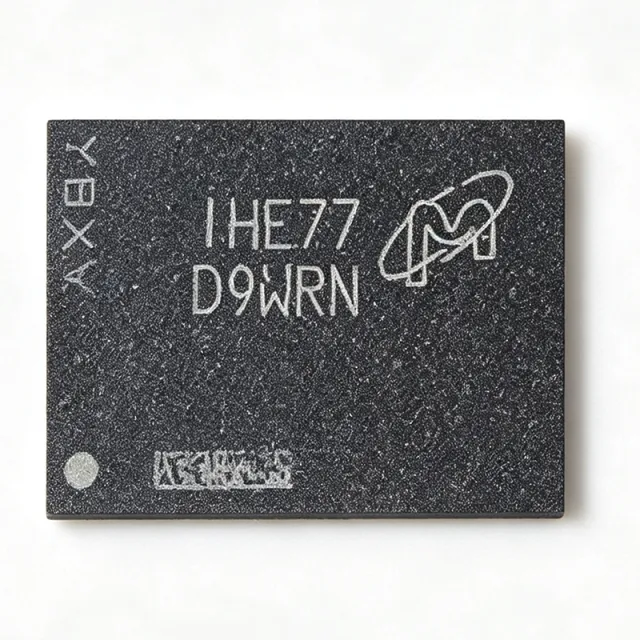
MT53E384M32D2DS-053 WT:E - 12Gbit LPDDR4 SDRAM | Micron
The Micron Technology MT53E384M32D2DS-053 WT:E is a 12Gbit mobile LPDDR4 SDRAM memory IC organized 384M x 32, operating at up to 1.866 GHz data rate in a 200-ball WFBGA (10 x 14.5 mm) package with Double Data Period (DDP) die architecture. Mobile LPDDR4 (Low Power Double Data Rate 4) SDRAM is a JEDEC-defined DRAM category optimized for battery-powered systems. Within the memory hierarchy, LPDDR4 sits in the mobile DRAM family alongside LPDDR4X and LPDDR5, descending from LPDDR3 and DDR3L. Compared with desktop DDR SDRAM, LPDDR4 trades absolute peak bandwidth for dramatically lower operating voltage and standby current, making it the dominant main-memory technology in smartphones, tablets, and embedded systems. Key features of this device include the 12Gbit total density implemented as two stacked 6Gbit die (DDP), a 32-bit data width, and a -053 speed grade corresponding to 1866 Mbps per pin. The WT:E suffix denotes the commercial-industrial operating temperature range and RoHS-compliant lead-free WFBGA packaging. The x32 organization simplifies memory controller interfacing for mid-range SoCs that do not use x16 split-bus topologies. Technically, the device uses a 1.1V-class core supply with LPDDR4 low-voltage swing I/O, bank-group architecture, and on-die termination to maintain signal integrity at gigabit-per-second data rates across the fine-pitch 200-ball array. Micron fabricates the part on a advanced DRAM process, and the DDP construction allows 12Gbit in a single footprint that historically held 8Gbit. Typical applications are mobile and IoT systems: smartphone and tablet main memory, automotive telematics and infotainment modules, networking equipment line-card buffers, and embedded vision or edge-AI platforms paired with application processors that integrate an LPDDR4 controller. A key design consideration is power-rail sequencing and VDDQ termination: LPDDR4 requires careful VDD1/VDD2/VDDQ rail management and fly-by-free point-to-point routing with controlled impedance to meet eye diagrams at 1866 Mbps. This page synthesizes distributor pricing and stock data, drop-in alternatives within the Micron LPDDR4 family, and practical design guidance not found in the manufacturer datasheet alone.
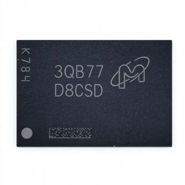
MT53E512M32D1ZW-046 - 16Gbit LPDDR4 SDRAM TFBGA-200 | Micron
The Micron Technology MT53E512M32D1ZW-046 is a 16Gbit (512M x 32) Mobile LPDDR4 SDRAM operating at up to 2.133 GHz with a 3.5 ns cycle time, housed in a 200-ball TFBGA (10 x 14.5 mm) package. Mobile LPDDR4 SDRAM is a low-power double-data-rate synchronous dynamic random-access memory optimized for battery-powered and thermally constrained systems. Within the memory hierarchy, it belongs to the DRAM family alongside DDR4 and LPDDR4X, distinguished by a 1.106 V nominal core voltage, deep power-down modes, and per-bank or all-bank refresh architectures that reduce idle power in smartphones, tablets, and embedded controllers. Key features include a wide x32 data bus for maximum bandwidth per chip-select, a built-in temperature sensor that drives self-refresh timing, auto precharge, write leveling, ZQ calibration, asynchronous reset, and data mask functions. The WT temperature grade covers -25C to +85C operation, while the D1 die provides 16Gbit of density in a single monolithic circuit. Architecturally, the device uses an 8n-prefetch pipeline with bank groups, delivering 2.133 Gb/s/pin data rates while maintaining low standby and deep-power-down currents. Dynamic voltage and frequency scaling, together with DVFS-compatible I/O termination, allows system designers to trade bandwidth against power in real time, which is essential for mobile SoC platforms and automotive infotainment stacks. Typical applications include smartphone and tablet main memory, automotive infotainment and ADAS SoC memory, industrial HMI panels, and networking equipment line-card buffers. The x32 organization suits SoCs with 32-bit memory controllers such as NXP i.MX, Rockchip, and Qualcomm embedded families. Design consideration: LPDDR4 requires per-device training of read/write leveling and DQS oscillation at every boot; ensure the SoC memory controller supports the -046 speed bin and that layout maintains length-matched, on-termination-capable fly-by routing. This page synthesizes distributor pricing, grade-level drop-in variants, and practical design notes not found in the manufacturer datasheet.

MT53E512M32D1ZW-046BAUT:B - 16Gbit LPDDR4X SDRAM | Micron
The Micron Technology MT53E512M32D1ZW-046BAUT:B is a 16 Gbit mobile LPDDR4X SDRAM memory IC organized as 512M x 32, operating at 2.133 GHz with a 3.5 ns access time, housed in a 200-ball TFBGA (10 mm x 14.5 mm) package. LPDDR4X SDRAM (Low Power Double Data Rate 4X synchronous dynamic random access memory) is a class of volatile DRAM optimized for mobile and embedded systems. Within the memory hierarchy it sits at the main-system-memory level, below CPU caches and above storage, and belongs to the broader JEDEC DDR SDRAM family. Compared with standard LPDDR4, the LPDDR4X variant lowers the I/O interface voltage (VDDQ) to approximately 0.6V, significantly reducing I/O power consumption, which is the dominant power draw at multi-gigabit data rates. Key features of this device include the 16 Gbit (2 GB) capacity in a single 32-bit-wide component, a parallel interface clocked at 2.133 GHz, and an automotive-grade AUT suffix designation. According to Microchip USA product data, the part is AEC-Q100 qualified and operates from a supply voltage range of 1.06V to 1.17V on the core rail, supporting the low-power behavior expected of the LPDDR4X family. Architecturally, the device is organized as 512M x 32 with internal banks accessed through a double-data-rate interface, allowing commands and data to be transferred on both clock edges for an effective 4266 MT/s class data rate. Deep power-down, self-refresh, and partial-array self-refresh style power management modes typical of Micron's MT53E mobile DRAM family minimize standby current in battery-operated systems. Typical applications include automotive infotainment and advanced driver assistance (ADAS) platforms, where AEC-Q100 qualification is mandatory, as well as high-performance embedded computing, industrial gateways, and networking equipment requiring dense DRAM in a compact footprint. A key design consideration is signal integrity: at 2.133 GHz operation, trace length matching, on-die termination (ODT) configuration, and VDDQ decoupling dominate the layout effort, and the memory controller must be configured for the LPDDR4X timing tables in the manufacturer datasheet. This page synthesizes distributor inventory data, drop-in alternatives, and practical design notes not found in the manufacturer datasheet alone.
MT53E512M32D2FW-046 - 16Gb LPDDR4 SDRAM 2133MHz | Micron
The Micron Technology MT53E512M32D2FW-046 AAT:D is a 16Gbit mobile LPDDR4/LPDDR4X SDRAM organized as 512M x 32, operating at 2133 MT/s (2.133 GHz) with a 5.3 GB/s peak data rate per pin, housed in a 200-ball TFBGA (10 mm x 14.5 mm) package. Mobile LPDDR (Low Power Double Data Rate) SDRAM is a class of DRAM optimized for low power consumption and high bandwidth in battery-powered and thermally constrained systems. Within the memory hierarchy, LPDDR4 sits under synchronous DRAM and power-management-aware memory ICs, and the unified LPDDR4/LPDDR4X die family allows the same hardware to run at 1.10V VDDQ (LPDDR4) or 0.60V VDDQ (LPDDR4X), dramatically reducing I/O power. Key features include a 16Gbit density in a single x32 die, 2133 MHz clock support (3.5 ns cycle time), dual-voltage operation covering both LPDDR4 and LPDDR4X protocols, and automotive-grade screening in the AAT:D temperature grade with operation from -40C to +105C. The die uses Micron LPDRAM process technology with bank-group architecture supporting eight internal banks, on-die termination, and standard LPDDR4 command timing per the JEDEC LPDDR4 interface (referenced generically per the manufacturer datasheet). The FW package's 10 mm x 14.5 mm footprint keeps routing short for high-speed 32-bit data buses in compact layouts. Typical applications include automotive infotainment and ADAS vision platforms, industrial HMI and edge-AI gateways, and high-performance embedded computing modules where 4 GB-class DRAM with low idle power is required. Design consideration: VDDQ selection (0.60V for LPDDR4X vs 1.10V for LPDDR4) must match the SoC memory controller configuration, and fly-by command/address routing requires per-byte line termination. This page synthesizes distributor availability, drop-in same-family alternatives, and practical design notes not found in the manufacturer datasheet. Pricing as of 2026-09-02.
MT53E512M64D2HJ-046 - 32Gbit LPDDR4X SDRAM | Micron | Mobile
The Micron Technology MT53E512M64D2HJ-046 is a 32 Gbit Mobile LPDDR4X SDRAM memory IC organized as 512M x 64, with a parallel interface, 2.133 GHz clock rate (3.5 ns access time) and a 556-ball WFBGA package measuring 12.4 mm x 12.4 mm. Mobile LPDDR4X (Low Power Double Data Rate 4X) SDRAM is a low-voltage DRAM derived from the LPDDR4 standard, optimized for battery-powered and thermally constrained systems. Within the memory hierarchy it sits under synchronous DRAM (SDRAM) -> mobile DRAM -> LPDRAM, and complements NOR/NAND flash in embedded and mobile platforms. LPDDR4X lowers the I/O termination voltage (VDDQ) relative to LPDDR4, reducing I/O power while preserving the LPDDR4 protocol and data rates. Key features of this device include the 32 Gbit density in a x64 organization, 4266 Mb/s data rate per pin enabled by the 2133 MHz clock, and the compact 556-ball FBGA (12.4 x 12.4 mm) footprint that supports space-limited SoC memory subsystems. Distributor listings cover industrial (AIT/AAT), automotive (AUT) and wide-temperature (WT) grade variants, allowing a common footprint across market segments. Architecturally, the device implements the LPDDR4/LPDDR4X mobile SDRAM protocol with bank groups and burst access, delivering the high bandwidth SoC application processors require. The parallel 64-bit data path minimizes the number of devices needed per system, simplifying routing compared to x32 organizations. Typical applications include automotive infotainment and ADAS platforms, industrial HMI and edge-compute modules, and networking/embedded systems where high-bandwidth, low-power DRAM is required alongside an application processor. Design consideration: LPDDR4X signal integrity demands length-matched fly-by routing, on-die-termination (ODT) tuning and careful VDDQ decoupling; follow the memory controller vendor's layout guide for the 556-ball FBGA footprint. This page synthesizes distributor pricing and stock data, same-footprint grade alternatives, and practical design notes not consolidated in the manufacturer part catalog.
MT53E768M32D2ZW-046 - 24Gbit LPDDR4X SDRAM 200-TFBGA | Micron
The Micron Technology MT53E768M32D2ZW-046 WT:C is a 24Gbit Mobile LPDDR4X SDRAM memory IC organized as 768M x 32, operating at 2.133 GHz data rate with LVSTL signaling, supplied in a 200-ball TFBGA package measuring 10 x 14.5 mm. LPDDR4X (Low Power Double Data Rate 4X) is a mobile-optimized SDRAM standard derived from the LPDDR4 JEDEC architecture. It belongs to the DRAM -> synchronous dynamic random-access memory -> volatile memory hierarchy and differs from standard DDR4 by using a lower VDDQ core I/O voltage (approximately 0.6V for LPDDR4X versus 1.2V for LPDDR4), which significantly reduces I/O power consumption in battery-operated systems. Key features include the 24Gbit (3 GB) single-die density, a 32-bit data bus, 3.5 ns clock cycle time, and the WT speed grade supporting 200/264 ball-out configurations. The LVSTL (Low Voltage Swing Termination Logic) interface reduces I/O switching power. A supply voltage range of 1.06V to 1.17V (VDD2) supports low-power operation. The device is available in commercial WT:C and automotive AAT:C/AIT:C grades, with the automotive variants qualified to AEC-Q100 and rated for operation down to -25C per distributor data. Micron manufactures this part on an advanced DRAM process, using bank-group architecture for high bandwidth efficiency at the 4266 MT/s class data rate of the -046 speed bin. Typical applications include smartphone and tablet main memory, automotive infotainment and ADAS domain controllers, edge AI compute modules, and embedded industrial systems that pair LPDDR4X with application processors from vendors such as Qualcomm, NXP i.MX, Rockchip, and MediaTek. Design consideration: LPDDR4X routing requires strict length matching on the 32-bit data bus, controlled impedance, and careful VDDQ decoupling; the Z ball-out requires a specific controller ball-map match, so verify your SoC memory controller supports the Z-die option before layout. This page synthesizes distributor pricing, same-package drop-in grade variants, design notes, and comparison data not found in the manufacturer datasheet.
MT53E768M32D4DT-046 - 24Gb LPDDR4 SDRAM x32 | Micron
The Micron Technology MT53E768M32D4DT-046 is a 24Gbit Mobile LPDDR4 SDRAM memory IC organized as x32, operating at a data rate of 2133 MT/s (2.133 GHz) in a 200-ball VFBGA package measuring 10 x 14.5 mm. Mobile LPDDR4 SDRAM is a low-power double-data-rate synchronous DRAM variant defined for battery-powered and thermally constrained systems. Within the memory hierarchy it sits under DRAM -> synchronous DRAM -> mobile LPDDR family, prioritizing low operating voltage and low standby power over the absolute bandwidth of desktop DDR4. LPDDR4 achieves this through reduced I/O swing, bank-group architecture, and deep power-down states. Key features of the MT53E768M32D4DT include a 24 Gbit total density (768 M x 32), a wide x32 data interface that simplifies 32-bit memory controller interconnects, and the -046 speed grade supporting 2133 MT/s operation. The VFBGA (Very Fine Pitch Ball Grid Array) 200-ball package saves board area versus discrete-drain packages and is standard for stacked mobile memory placement. Architecturally, the device uses the LPDDR4 bank-group structure, allowing back-to-back data access across bank groups to sustain the 2133 MT/s bus rate. Command/address and data interfaces run at point-to-point connections typical of LPDDR4 systems, with terminating on-die termination (ODT) schemes to preserve signal integrity at high data rates. Typical applications include i.MX8-class application processor memory subsystems (NXP community reports 8 GB configurations with MT53E768M32D4DT passing stress tests on i.MX8QM), mobile and wearable devices, industrial HMIs, and automotive infotainment platforms using the AAT:E automotive variant. A key design consideration: LPDDR4 requires controller tuning of read/write preamble, ODT values, and drive strength during memory training; migrating from an older MT53B LPDDR4 part at 1600 MT/s to this -046 grade requires raising the DDR PLL from 800 MHz to 1066 MHz in firmware. This page adds value beyond the datasheet by synthesizing distributor pricing and stock, pin/package cross-references, firmware migration notes, and practical alternatives in one place.
MT53E768M32D4DT-053 - 24Gbit LPDDR4 4266Mbps x32 | Micron
The Micron MT53E768M32D4DT-053 is a 24Gbit (3GB) Mobile LPDDR4 SDRAM memory IC organized as 768M x32, operating at up to 1.866 GHz clock frequency (4266 Mbps/pin data rate) in a 200-ball VFBGA (10 x 14.5 mm) package. This quad-die package (QDP) LPDRAM targets flagship smartphones, tablets, automotive infotainment, and high-performance embedded systems requiring maximum density in a mobile-optimized footprint. LPDDR4 (Low Power Double Data Rate 4) is a JEDEC-defined synchronous DRAM interface standard optimized for mobile and low-power computing. Within the memory hierarchy, it sits below DDR4 server memory in absolute bandwidth but delivers superior performance-per-watt, lower operating voltage (VDDQ = 1.1 V), and a smaller ball pitch, making it the dominant DRAM type for battery-powered SoC platforms. Key features include 24Gbit density in a single component, 32-bit data width, 1.866 GHz maximum clock, low-voltage 1.1 V I/O signaling, and Micron's quad-die package construction that stacks four 6Gbit dice to achieve density without enlarging the footprint. Temperature-grade suffix options (WT commercial, AIT industrial, AUT automotive) let designers qualify one layout across multiple environments. The LPDDR4 architecture uses bank-group based 8n prefetch, on-die termination, and DBI (data bus inversion) to reduce power and improve signal integrity at 4266 Mbps. DPD (deep power down) and self-refresh modes minimize standby current in always-on mobile designs. The -053 speed grade supports the highest LPDDR4 bin, enabling full-rate operation with flagship SoCs. Typical applications include smartphone and tablet application processor memory, automotive infotainment and ADAS domain controllers, networking appliances, and industrial HMI platforms where 3GB of DRAM in a compact 10 x 14.5 mm VFBGA is required. When designing with this part, follow JEDEC LPDDR4 routing practice: length-match the 32-bit data bus, use on-die termination settings from the mode register programming guide, and verify ZQ calibration resistor placement per the Micron datasheet. This page synthesizes verified distributor listings, drop-in speed/temp-grade alternatives, and practical design notes not found in the manufacturer part catalog.

MT58L64L32PT7.5 - 2Mbit Sync Burst SRAM 133MHz | Micron
The Micron MT58L64L32PT7.5 (also written MT58L64L32PT-7.5) is a 2Mbit synchronous pipelined burst SRAM memory organized as 64K x 32 bits, delivering a 4 ns access time and 133 MHz clock operation in a 100-pin TQFP (14 x 20.1 mm) surface-mount package. It operates from a 3.135V to 3.6V supply, consistent with a 3.3V LVTTL system interface. A synchronous burst SRAM is a type of static random-access memory that uses an external clock to synchronize address, data, and control signals, providing deterministic zero-wait-state access for processors and controllers. Within the memory hierarchy, SRAM sits above DRAM in speed (no refresh required) and is commonly used as cache or high-speed buffer memory in power management and data-path subsystems. The Micron SYNCBURST family implements a pipelined architecture in which the address is registered on the clock edge, allowing a short clock-to-data cycle while sustaining full-bandwidth back-to-back transfers. Key features of the MT58L64L32PT-7.5 include the 64K x 32 organization suited to 32-bit buses without byte-lane fan-out, 133 MHz operation with 4 ns clock-to-data access, burst address counter supporting linear and interleaved burst orders for x86 and PowerPC style bus protocols, and a synchronous burst control set (clock enable, address advance, output enable, byte write enable). The 3.3V core with LVTTL I/O simplifies interfacing with 1990s-to-2000s era CPUs, FPGAs, and ASICs. The pipelined architecture registers inputs internally, trading one cycle of latency for higher sustainable clock frequency. Data valid timing is governed by the 4 ns access time relative to the clock edge, enabling 133 MHz (7.5 ns cycle) operation with standard setup and hold margins. JEDEC-standard 100-lead TQFP packaging with 0.5 mm lead pitch supports conventional reflow assembly. Typical applications include cache memory for embedded PowerPC and MIPS processors, FPGA design buffers and look-up expansion memory, telecommunications and networking line-card buffers, and test/measurement instrumentation where deterministic latency matters more than density. Design-wise, ensure all unused address inputs are properly driven and decouple VDD with 0.1 uF ceramics at each power pin; synchronous inputs must meet datasheet setup/hold times relative to CLK, and floating controls cause undefined operation. This page synthesizes distributor pricing, drop-in family alternatives, and practical design notes not found in the manufacturer datasheet.

MT62F1536M64D8EK-023 - 96Gbit LPDDR5X SDRAM | Micron | Mobile
The Micron Technology MT62F1536M64D8EK-023 is a 96 Gbit Mobile LPDDR5X SDRAM memory IC organized as 1.5G x 64, operating at a clock frequency of 4.266 GHz with LVSTL (Low Voltage Swing Terminated Logic) memory interface signaling, housed in a 441-ball TFBGA (14 x 14 mm) package. LPDDR (Low Power Double Data Rate) SDRAM is a class of DRAM optimized for mobile and power-sensitive computing systems, sitting within the memory hierarchy as a main-memory solution beneath the broader DRAM family that also includes DDR4, DDR5, and GDDR variants. Unlike desktop DDR memory, LPDDR devices trade raw peak throughput per channel for significantly lower operating voltage and standby power, which is why they dominate smartphone, tablet, and edge-compute designs. Key features of this device include the LPDDR5X interface supporting data rates up to 4.266 GHz (4266 MT/s class), a narrow supply voltage window of 1.01 V to 1.12 V on the core rail, and the 441-ball fine-pitch TFBGA (14 x 14 mm) footprint that enables dense PoP or discrete mounting on mobile PCBs. The x64 bus organization allows a single package to serve as a complete 12 GB memory solution in wide-bus SoC platforms. At the silicon level, the device uses LVSTL signaling, which reduces I/O voltage swing relative to earlier SSTL/POD interfaces, cutting both dynamic I/O power and signal-integrity margins required at multi-gigabit data rates. The -023 speed bin places the part in the highest-frequency LPDDR5X tier, suitable for flagship mobile SoCs, AI accelerators at the edge, and high-bandwidth embedded processors. Typical applications include flagship smartphone main memory, tablet and notebook LPDDR5X memory subsystems, automotive infotainment and ADAS platforms (via the automotive AAT/AUT/AIT grade variants), and edge AI modules where 96 Gbit of low-power DRAM bandwidth is required next to an SoC. Design considerations: LPDDR5X routing requires careful length matching of the CA and DQ bus, and the 1.01 V to 1.12 V core supply demands a tight-tolerance PMIC with VDDQ dynamic voltage scaling support. Verify the exact grade suffix (WT, AAT, AIT, AUT) against your temperature and qualification requirements before layout freeze. This page synthesizes distributor pricing, drop-in grade-variant alternatives, and practical design notes not found in the manufacturer datasheet alone.
MT62F3G32D8DV-023 - 96Gb LPDDR5X SDRAM 4266Mbps | Micron
The Micron Technology MT62F3G32D8DV-023 is a 96Gbit (12GB) LPDDR5X SDRAM mobile memory IC organized as 3G x 32, operating at 4.266 GHz data rate (4266 Mbps/pin) over an LVSTL (Low Voltage Swing Terminated Logic) interface, housed in a 315-ball LFBGA package measuring 12.4 mm x 15 mm. LPDDR5X (Low Power Double Data Rate 5X) is the extended-speed evolution of the LPDDR5 JEDEC mobile DRAM standard, used across the memory hierarchy in smartphones, tablets, and edge-AI computing platforms. LPDDR SDRAM sits within the broader DRAM family alongside DDR SDRAM and GDDR, and it is distinguished by aggressively reduced supply voltages, deep power-down states, and per-bank refresh optimized for battery-powered systems. Key features of the MT62F3G32D8DV-023 include a 96Gbit density in a single die-composed package, a 32-bit wide data bus, LVSTL signaling at 4266 Mbps per pin, and industrial temperature support in the AIT (automotive/industrial temperature) speed-grade variants. The WT (commercial wide-temperature) grade supports -25C to +85C operation per distributor listings. Backward compatibility with LPDDR5 controllers at reduced rates simplifies platform integration where LPDDR5X speed is not required. Architecturally, the device uses Micron LPDDR5X core technology with bank-group organization, on-die termination, and dynamic voltage-frequency scaling support characteristic of the LPDDR5/5X generation, enabling high effective bandwidth of approximately 136.5 Gbps aggregate on a 32-bit bus (4266 Mbps x 32). Typical applications include flagship smartphone and tablet main memory, AI edge accelerators, automotive infotainment and ADAS compute platforms (AIT grade), 5G modems, and high-performance IoT gateways. Design consideration: LPDDR5X routing demands careful length matching and reference-plane discipline for the 4266 Mbps LVSTL interface; SoC controller training algorithms must be verified against Micron's speed-grade binning before locking timing parameters. This page synthesizes distributor pricing, same-family drop-in alternatives, and practical design notes not consolidated in the manufacturer datasheet.

MT62F512M64D2CZ-023FAUT:E - 32Gbit LPDDR5X SDRAM | Micron
The Micron Technology MT62F512M64D2CZ-023FAUT:E is a 32 Gbit mobile LPDDR5X SDRAM memory IC with a 64-bit data organization, LVSTL I/O interface, and a maximum data rate of 4.266 GHz (4266 Mbps/pin), housed in a 561-ball TFBGA package measuring 8 x 12.4 mm. LPDDR5X (Low Power Double Data Rate 5X) is an extension of the LPDDR5 DRAM standard defined by JEDEC, engineered for mobile, automotive, and edge-AI systems that require both high bandwidth and minimal power draw. As the highest-performance member of the low-power DRAM family, LPDDR5X raises the I/O speed ceiling beyond LPDDR5 while retaining the same command architecture and ballout, making it the dominant main-memory choice for flagship smartphones, ADAS domain controllers, and AI accelerators. Key features of this device include 32 Gbit (4 GB) of DRAM density in a single package, a 64-bit wide bus that yields roughly 34 GB/s of aggregate bandwidth at full speed, and the low-voltage LVSTL 0.5 I/O signaling class that reduces switching power versus LPDDR4X. The -023 speed grade designates operation at the 4.266 GHz data-rate class, and the :E suffix denotes Micron lead-free, RoHS-compliant termination. Automotive designation (AUT, per Newark listed as AEC-Q100 DRAM, Mobile LPDDR5X) targets harsh-environment designs requiring qualified supply continuity. Architecturally, the device inherits the LPDDR5X deep-power-down, per-bank refresh, and dynamic voltage-frequency scaling features, letting system controllers trade performance for power on the fly. The 561-ball TFBGA with 0.5 mm-class ball pitch supports standard mobile PCB stacking and PoP-adjacent layouts near an application processor. Typical applications include automotive ADAS/autonomous-driving compute platforms, flagship smartphone and tablet main memory, AI edge inference modules, and high-performance embedded vision systems. In each case the combination of 32 Gbit density, 64-bit width, and 4266 Mbps/pin data rate delivers the memory bandwidth that modern SoCs demand. Design consideration: LPDDR5X signal integrity requires careful length-matched routing and power integrity; consult the Micron datasheet for VDD/VDDQ termination and fly-by topology requirements before layout. This page synthesizes distributor availability data, same-package drop-in variants, and practical design notes beyond what the manufacturer datasheet alone provides. Pricing references are as of 2026-09-02.
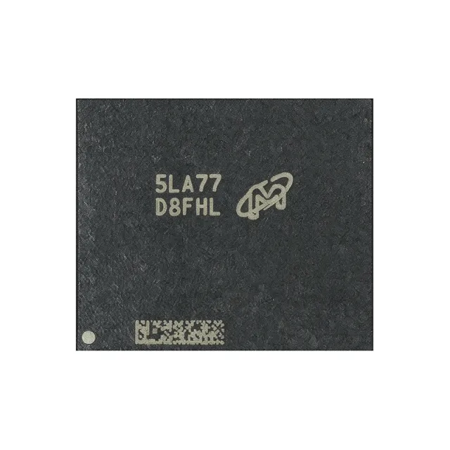
MT68A512M32DF-28:A - GDDR7 16Gbit 28Gbps | Micron
The Micron MT68A512M32DF-28:A is a 16Gbit (2GB) GDDR7 SDRAM graphics memory IC organized as 32-bit, operating at an effective data rate of 28 Gbps, housed in a 266-ball TFBGA (Fine-Pitch Ball Grid Array) package. As of 2026-10-11 the device has been designated End of Life by Micron alongside its 32 Gbps sibling MT68A512M32DF-32:A. GDDR7 (Graphics Double Data Rate 7) is the latest generation of high-bandwidth graphics DRAM, succeeding GDDR6 and GDDR6X. Graphics DRAM sits within the broader memory hierarchy of volatile semiconductor memory: DRAM -> synchronous DRAM -> graphics DRAM -> GDDR family. Unlike DDR5, which prioritizes capacity per channel for CPUs, GDDR prioritizes aggregate bandwidth for GPU workloads, using wider per-device interfaces and PAM3 signaling introduced in the GDDR7 generation to raise per-pin data rates. Key features of this device include the 16 Gbit density (2GB per chip), a 32-bit memory organization, and the 28 Gbps data rate, which matches the memory speed used by NVIDIA GeForce RTX 50 series cards such as the RTX 5060. The TFBGA package provides the short, controlled-impedance ball-out required for multi-gigabit signal integrity on graphics PCBs. Architecturally, GDDR7 devices retain a SDRAM-style bank/row/column core while adopting PAM3 (3-level pulse amplitude modulation) I/O, which transmits three bits over two cycles and reduces the required clock frequency relative to NRZ signaling at equivalent bandwidth. This lowers power and EMI at 28 Gbps while supporting the trainability and error-tolerance features expected in modern GPU memory subsystems. Typical applications include discrete graphics cards for gaming and workstation platforms, AI inference accelerators, video capture and broadcast equipment, and high-performance edge computing modules that require multi-hundred-GB/s memory bandwidth per chip. A key design consideration is supply chain risk: this exact part was marked EOL in September 2026 as Micron shifts 2GB GDDR7 capacity to denser 24Gb (3GB) devices, so new designs should qualify alternate density or speed grades early and secure last-time-buy inventory. This page synthesizes distributor listings, lifecycle reporting, and drop-in alternative guidance not found on a single manufacturer page, providing engineers a consolidated sourcing and design view.
MTC20F2085S1RC48BR - 32GB DDR5-4800 ECC RDIMM | Micron
The Micron Technology MTC20F2085S1RC48BR is a 32GB DDR5-4800 ECC Registered DIMM (RDIMM) server memory module operating at 1.1V with CL40 CAS latency, dual-rank x8 organization (2Rx8), in a 288-pin registered dual in-line memory module form factor. A Registered DIMM (RDIMM) is a type of memory module used in servers and workstations in which address and command signals are buffered by a register chip between the memory controller and the DRAM devices. This buffering reduces electrical loading on the memory controller, allowing higher-capacity and higher-density memory populations than unbuffered UDIMMs. RDIMMs sit within the memory module hierarchy of DRAM -> DDR5 SDRAM -> registered memory module, and they include on-module ECC (Error Correction Code) to detect and correct single-bit memory errors for data integrity. Key features of the MTC20F2085S1RC48BR include 32GB capacity in a dual-rank x8 configuration, PC5-38400 bandwidth at DDR5-4800 data rates, CL40 CAS latency, and 1.1V operation that lowers power consumption versus DDR4 equivalents. DDR5 moves the power management to an on-module PMIC (Power Management IC) and doubles bank groups versus DDR4, improving effective bandwidth and channel efficiency. Technically, this RDIMM uses registered address/command signaling with ECC, making it suitable only for server platforms with registered-memory controllers. It is NOT compatible with desktop UDIMM slots and cannot be mixed with unbuffered or load-reduced (LRDIMM) modules in the same channel. Typical applications include general-purpose server hosts, edge compute nodes, virtualization hosts with moderate VM density, and OEM server builds from vendors such as Dell PowerEdge and HPE ProLiant platforms using Intel Xeon Scalable (including Sapphire Rapids) processors. Design consideration: always populate memory channels symmetrically per the platform OEM memory population rules, and verify BIOS/UEFI support for DDR5-4800 at the installed CPU; data rate may derate at higher DIMM populations. This page synthesizes distributor pricing, verified cross-references to OWC and NEMIX replacement modules, and practical deployment notes not consolidated in the manufacturer datasheet.
MTFDKBA960TFR-1BC1ZABYY - 960GB NVMe Gen4 M.2 2280 SSD | Micron 7450 PRO
The Micron MTFDKBA960TFR-1BC1ZABYY is a 960 GB data-center-class NVMe SSD in the M.2 2280 (22 x 80 x 3.8 mm) form factor, part of the Micron 7450 PRO series built on 176-layer TLC NAND. The drive presents a PCIe Gen4 x4 NVMe 1.4 interface and is rated for read-intensive workloads, delivering sequential read performance up to 4000 MB/s and sequential write up to 1120 MB/s per the Arrow distributor listing. The PRO variant in this part number is non-SED (no self-encrypting drive silicon), making it appropriate for read-heavy workloads where hardware encryption is not a regulatory requirement. A data center NVMe SSD is a high-performance non-volatile storage device that uses the NVM Express protocol over a PCIe physical layer to deliver low-latency, high-IOPS access to host systems. The 7450 PRO belongs to Micron's third-generation data center NVMe family and uses the same NVMe 1.4 base specification as enterprise-grade SSDs from Kioxia, Samsung, and Solidigm. Within the storage hierarchy, M.2 NVMe SSDs sit between SATA SSDs (lower throughput) and U.2 / EDSFF enterprise NVMe drives (higher capacity and hot-swap features). The 7450 PRO is designed specifically for read-intensive workloads in hyperscale and mainstream data center deployments. Key features include 176-layer Micron TLC NAND, an in-house controller with PCIe Gen4 x4 NVMe 1.4, hot-plug capability, power-loss protection through the 12 V rail, and OCP-compliant telemetry. The drive supports a 1 DWPD endurance class (typical for read-intensive PRO variants) and is qualified for the Open Compute Project (OCP) NVMe Cloud SSD specification, easing integration into hyperscale racks. A M.2 2280 form factor means it drops directly into the standard M.2 socket found on most modern server motherboards and backplanes without cabling. Typical applications include boot drives for hyperscale data center servers, read-heavy caching tiers in front of large capacity HDD pools, NoSQL database acceleration (Aerospike, RocksDB, Cassandra), and edge compute nodes requiring low-latency NVMe storage in a compact M.2 envelope. The 7450 PRO's low power envelope and standard M.2 2280 form factor also make it suitable for OCP-compliant microserver platforms. Design considerations: ensure your host M.2 slot provides PCIe Gen4 x4 lanes rather than Gen3 or x2, otherwise peak bandwidth will be limited. M.2 NVMe SSDs dissipate up to approximately 8 W under sustained write workloads, so motherboard airflow across the M.2 slot is critical - consider an M.2 heatsink for sustained workloads. Verify that your BIOS/EFI has NVMe 1.4 support enabled; older NVMe 1.2-only stacks can still enumerate the drive at reduced performance. This page synthesizes distributor pricing, NVMe 1.4 datasheet references, and practical deployment guidance not aggregated on a single datasheet page.
MTFDKCC15T3TGH-1BC1ZABYY - 15.36TB 9400 PRO NVMe U.3 SSD
The Micron MTFDKCC15T3TGH-1BC1ZABYY is a 9400 PRO 15.36 TB enterprise NVMe solid-state drive in the U.3 (15 mm) 2.5-inch form factor, with a PCIe Gen4 x4 host interface and TLC 3D NAND. It is part of Micron's data-center SSD portfolio tuned for read-intensive workloads at 1 DWPD endurance. An enterprise NVMe SSD is a high-performance non-volatile storage device that connects to the host system via the Non-Volatile Memory Express protocol over a PCIe physical layer, bypassing legacy SAS/SATA controller overhead. Within the broader storage hierarchy, NVMe SSDs sit between DRAM (volatile, fastest) and SATA SSDs/HDDs (slower, larger capacity), and they are categorized as data-center SSDs (DC SSDs) when qualified for 24/7 mixed-workload server operation. The 9400 PRO family specifically targets read-intensive, capacity-dense workloads such as object stores, content delivery, and large-scale analytics. Key features of the MTFDKCC15T3TGH-1BC1ZABYY include a usable capacity of 15.36 TB, PCIe Gen4 NVMe 1.4 interface, sequential read performance up to 7,000 MB/s and sequential write up to 7,000 MB/s (class-leading for capacity), random 4 KB read up to 1.1M IOPS, and 1 DWPD endurance rated for five years. The drive uses Micron's 176-layer TLC NAND and ships in the 70 x 100 x 15 mm U.3 (SFF-TA-1001) hot-swap form factor, supporting U.3 backplane interoperability with U.2 hosts via adapter. Architecturally, the 9400 PRO leverages a multi-core NVMe controller with hardware-accelerated LDPC ECC, end-to-end data-path protection (PLP), and dynamic namespace management. PCIe Gen4 doubles per-lane throughput versus Gen3, and combined with 16 NAND channels this unlocks the dual 7 GB/s read/write figure. AES-256 hardware encryption, TCG Opal 2.0 (where ordered), Sanitize and Format NVM commands, and power-loss protection make it suitable for enterprise security and compliance frameworks. Typical applications include hyperscale object storage (Ceph, S3-compatible), AI/ML training data lakes, video streaming and CDN edge caches, database warehousing, VMware vSAN capacity tiers, and read-heavy analytics workloads. The 1 DWPD rating means it is best fitted to read-dominated rather than write-heavy log or database primary storage. When designing with this drive, ensure the host backplane supports the U.3 (SFF-TA-1001) connector; legacy U.2 (SFF-8639) backplanes remain compatible via dual-mode pinout. Confirm platform BIOS/UEFI NVMe driver support and thermal envelope (typically up to 25 W active) - server front-panel airflow above 1.5 m/s is recommended at full load. This page synthesizes distributor pricing, drop-in alternatives drawn from the verified web cross-reference, and practical design notes for data-center SSD selection not found in a single datasheet.
MTFDKCC6T4TFS-1BC1ZABYY - 6.4TB U.3 NVMe Data Center SSD | Micron
The Micron MTFDKCC6T4TFS-1BC1ZABYY is a 6.4 TB U.3 (15 mm) NVMe data-center SSD from the 7450 MAX family, featuring 176-layer TLC NAND, PCIe Gen 4 x4 host interface, and a mixed-use endurance rating, optimized for read/write-intensive enterprise workloads. It ships as a non-SED (no hardware encryption) 2.5-inch module. A U.3 NVMe SSD is a small-form-factor enterprise storage device that combines the hot-plug 2.5-inch mechanical envelope of SAS/SATA SSDs with the high-bandwidth NVMe protocol, enabling up to ~7 GB/s sequential reads over PCIe Gen 4 x4. The 7450 MAX line sits at the top of Micron's 7450 stack for mixed-use endurance, below the PRO (read-intensive) and above entry NVMe data-center parts. As a data-center SSD it belongs to the hierarchy: NAND flash module -> NVMe SSD -> enterprise storage -> data-center infrastructure, and uses Micron's 176-layer replacement-gate TLC NAND paired with an in-house controller for predictable QoS under heavy random IO. Key features include 6.4 TB raw TLC capacity, PCIe Gen 4 x4 NVMe interface, 176-layer NAND technology, and a 15 mm U.3 form factor (70 x 100 mm). The "MAX" classification indicates a higher drive-writes-per-day rating than PRO siblings, making this SKU appropriate for mixed read/write database and virtualization workloads rather than purely read-intensive archival use. The drive leverages Micron's vertical 7450 architecture that combines a PCIe Gen 4 controller, DRAM cache, and 176-layer NAND into a single 15 mm U.3 module. The MAX endurance class targets sustained random write workloads in databases such as SQL Server, Oracle, MySQL, RocksDB, Cassandra, and Aerospike, where IOPS/Watt and predictable tail latency matter more than raw sequential bandwidth. Typical applications include hyperscale data-center boot drives, mixed-use database acceleration (SQL, Oracle, NoSQL), virtualization and VDI storage tiers, software-defined storage nodes, AI/ML training data caches, and high-performance edge-compute servers. The U.3 form factor is drop-in compatible with U.2 backplanes that support NVMe Gen 4, simplifying fleet upgrades. When designing with this drive, ensure the host backplane supports PCIe Gen 4 x4 and provides adequate airflow - sustained mixed-use workloads generate meaningful heat inside the 15 mm chassis. Drive firmware should be kept current via Micron's Storage Executive utility, and SMART attributes should be monitored for endurance (percentage used) in production fleets.
MTFDKCC7T6TFR-1BC1ZABYY - 7.68TB U.3 NVMe Data Center SSD | Micron
The Micron MTFDKCC7T6TFR-1BC1ZABYY is a 7.68TB enterprise-class NVMe SSD from the 7450 PRO series, designed in a 2.5-inch U.3 (15mm) form factor with PCIe Gen4 x4 interface. Built on Micron's 176-layer TLC NAND technology, this non-SED drive delivers high sequential read performance suitable for read-intensive data center workloads. The drive targets cloud-scale and enterprise deployments where predictable latency and high throughput are critical. A U.3 (SFF-TA-1001) NVMe SSD is a 2.5-inch enterprise storage device that uses the PCIe interface to deliver significantly higher performance than SATA SSDs. U.3 (also known as U.2 backwards-compatible) supports hot-swap and tri-mode operation (NVMe/SATA/SAS) on compatible backplanes. The Micron 7450 PRO family uses TLC NAND with a 1 DWPD (Drive Write Per Day) endurance rating, positioning it for read-intensive workloads like content delivery, streaming, and boot drives. Key features of the MTFDKCC7T6TFR-1BC1ZABYY include PCIe Gen4 x4 NVMe 1.4 interface, 7.68TB usable capacity, 176-layer TLC NAND, and a 1 DWPD endurance rating for 5 years. The drive operates on a 12V supply and supports enterprise features such as power-loss protection, end-to-end data protection, AES-256 encryption (non-SED variant), and SMART/OCP-compliant telemetry. The U.3 15mm form factor provides robust thermal dissipation for sustained workloads. The 7450 PRO SSD uses Micron's proprietary controller and firmware stack, which implements advanced LDPC error correction and adaptive thermal throttling. The drive's latency profile is tuned for consistent QoS under mixed random read/write workloads, which is critical for virtualization and database deployments. PCIe Gen4 doubles the per-lane bandwidth of Gen3, enabling the 7450 to saturate the interface on sequential transfers. Typical applications include cloud-scale object storage, CDN edge caches, virtual desktop infrastructure (VDI) boot drives, read-intensive databases, AI/ML training data staging, and hyperscaler primary storage tiers. The 7.68TB capacity point is the most common for read-intensive workloads in the 7450 family. When designing with this drive, ensure the host platform supports U.3 hot-swap backplanes with proper PCIe bifurcation for x4 lanes. Validate firmware compatibility with the system BMC and OCP profile support for telemetry. For write-intensive workloads, consider the 7450 MAX (3 DWPD) variant instead. This page synthesizes distributor pricing, drop-in alternatives, and practical deployment notes not found in the manufacturer datasheet.
MX25L51245GXDI-08G - 512Mbit SPI NOR Flash 166MHz | Macronix
The Macronix MX25L51245GXDI-08G is a 512Mbit (64 MByte) 3V CMOS serial NOR Flash memory with Quad I/O, QPI, and DTR (Double Transfer Rate) support, running at up to 166 MHz in a 24-ball CSPBGA (6x8) package. It is organized as 64M x 8-bit and operates from a 2.7V to 3.6V supply. Serial NOR Flash is a non-volatile memory category within the broader flash memory hierarchy (NOR Flash -> flash memory -> semiconductor memory -> non-volatile memory IC). Unlike parallel NOR, serial NOR devices communicate over an SPI (Serial Peripheral Interface) bus, trading raw bandwidth for a much smaller pin count, smaller footprint, and lower system cost. Serial NOR is the dominant boot memory technology for embedded processors, FPGAs, microcontrollers, and networking SoCs. Key features of the MX25L51245G family include the MXSMIO (Serial Multi I/O) interface supporting x1, x2, and x4 I/O operation, QPI (Quad Peripheral Interface) mode for reduced command overhead, and DTR (Double Transfer Rate) mode that transfers data on both clock edges to maximize sequential read throughput. The device offers 100,000 program/erase cycles endurance and 20-year data retention per Macronix data. Technical depth: the XDI-08G speed grade supports a 166 MHz clock in Quad/DTR modes, enabling high read bandwidth for XIP (execute-in-place) code shadowing and fast FPGA configuration loading. Page program time is 750 microseconds with 60-microsecond word program support, and the architecture supports sector and block erase for flexible firmware update management. Typical applications include FPGA configuration/boot memory for Xilinx and Intel devices, embedded processor code storage in networking equipment, set-top boxes and automotive infotainment, and firmware storage in industrial controllers where high-density non-volatile code storage is required. Design consideration: verify VCC ramp and use the RESET#/hold features per the Macronix datasheet to ensure correct power-up state, and allocate proper decoupling at the 2.7V-3.6V supply pins. This page synthesizes distributor pricing, drop-in alternatives, pinout guidance, and practical design notes not found in the manufacturer datasheet alone.
MZ7WD480HCGM-00003 - Samsung SM843TN 480GB SATA SSD | 2.5" Enterprise
The Samsung MZ7WD480HCGM-00003 is the Samsung SM843TN enterprise-grade 2.5" SATA III (6 Gb/s) solid-state drive with a 480 GB capacity, utilizing Samsung's 20 nm MLC NAND flash and a proprietary Samsung controller. It is engineered for read-intensive data-center workloads, delivering sequential read performance up to 530 MB/s and sequential write performance up to 360 MB/s, with a 7 mm z-height that fits standard 2.5" server bays. A solid-state drive (SSD) is a data storage device that uses non-volatile flash memory (typically NAND) to persist data, replacing rotating hard disk drives (HDDs). SSDs sit in the storage hierarchy between DRAM caches and HDDs, offering orders-of-magnitude lower latency and much higher IOPS per watt. Enterprise SATA SSDs occupy the mainstream product-tier performance slot, balancing cost per GB against throughput and endurance; they fall under the broader category of NAND flash storage -> persistent memory -> data storage device -> computer hardware. Key specifications include 1.8 DWPD (drive writes per day) endurance rating over a 5-year warranty period, SED (Self-Encrypting Drive) support via TCG-Enterprise, power-loss data protection through onboard tantalum capacitors, and a sustained random 4 KB read IOPS figure suited for online transaction processing and virtual-desktop infrastructure (VDI) boot storms. The drive conforms to the SATA 3.2 specification and supports ATA-8 ACS command set, SMART monitoring, and NCQ (Native Command Queuing). The SM843TN architecture pairs Samsung's PX-series enterprise controller with MLC NAND and a DRAM cache buffer, achieving predictable latency under mixed read/write workloads typical of read-intensive applications. Power-loss protection circuitry uses the energy stored in capacitors to flush the in-flight write cache to NAND, preventing data corruption during unexpected power events — a critical feature for database and virtualization tiers. Typical deployment scenarios include read-intensive database servers, VDI boot images, content delivery network (CDN) edge caches, web-server front-end tiers, and email/messaging archive storage where sequential read throughput, predictable latency, and SED security outweigh the need for high write endurance. The 480 GB capacity is well-matched to boot partitions, indexing databases, and per-VM virtual-disk provisioning. When integrating this drive, verify that the host backplane supports SATA 6 Gb/s (SATA III) to achieve the rated 530 MB/s sequential read speed; legacy SATA II (3 Gb/s) hosts will throttle sequential throughput. For RAID arrays, match with other SM843T/SM843TN drives of identical firmware to avoid compatibility warnings on enterprise controllers (LSI/Broadcom, MegaRAID).

N24RF04DWPT3G - Dual Interface 4Kb EEPROM RFID NFC Tag | onsemi
The onsemi N24RF04DWPT3G is a dual-interface RFID/NFC tag IC with a 4 Kb EEPROM, an ISO/IEC 15693 contactless RF interface at 13.56 MHz, and an I2C contact interface operating from 1.8 V to 5.5 V, housed in an 8-pin SOIC (0.154 in, 3.90 mm width) package. A dual-interface EEPROM tag belongs to the family of memory ICs that combine passive radio-frequency access with a wired bus. The RFID/NFC tag hierarchy runs: dual-interface EEPROM tag -> RFID transponder IC -> RF memory IC -> memory IC -> semiconductor. The N24RF04 allows a reader (contactless, energy harvesting from the RF field) and a host microcontroller (contact, externally powered) to access the same non-volatile memory, enabling board-level identification, configuration storage, and traceability. Key features include the 4 Kb (512-byte) EEPROM organized with user and system blocks, ISO/IEC 15693 and ISO 18000-3 protocol support, NFC Forum Type 5 tag interoperability, an energy-harvesting output that can power small companion circuits, and data verification mechanisms for write integrity. The I2C interface requires an external supply and supports standard bus communication with any microcontroller, according to the onsemi N24RF04 datasheet. Technically, the device rectifies the 13.56 MHz carrier from the reader antenna coil connected between the AC0 and AC1 pins, regulates it to an internal supply, and manages read/write cycles to the EEPROM with error checking. The dual-interface arbitration ensures memory consistency regardless of which port accesses the data, a critical feature when both a reader and an MCU may write the same blocks. Typical applications include consumable identification and authentication in printers and medical cartridges, board-level manufacturing traceability, parameter storage for replaceable modules, and NFC-enabled configuration of industrial and IoT devices. When designing, keep the antenna loop close to the AC0/AC1 pins and respect the I2C supply requirement: the contact interface cannot rely on harvested field energy. Choose pull-up values for SDA/SCL appropriate to the 1.8 V to 5.5 V supply domain. This page synthesizes distributor pricing, drop-in alternatives, and practical design notes not found in the manufacturer datasheet.