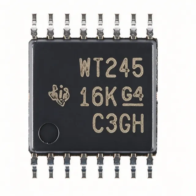
SN74AVC4T245PWR - 4-Bit Dual-Supply Level Shifter | TI
N.º de pieza: SN74AVC4T245PWR ✓ Activo| Cant. | Precio unitario | Total |
|---|---|---|
| 1 | $0.72 | $0,72 |
| 10 | $0.63 | $6,30 |
| 100 | $0.51 | $51,00 |
| 500 | $0.44 | $220,00 |
| 1.000 | $0.38 | $380,00 |
SN74AVC4T245PWR Descripción general
A bus transceiver is a digital integrated circuit that transfers data bidirectionally between two buses, using direction-control and output-enable inputs plus 3-state outputs so multiple devices can share a common bus. The SN74AVC4T245 belongs to the voltage translator (level shifter) family within the broader logic IC and interface IC hierarchy, and it is essential in mixed-voltage systems where MCUs, FPGAs, sensors, and memory operate at different logic levels.
Key features include configurable voltage translation on both ports, control inputs (1DIR, 2DIR, 1OE, 2OE) referenced to VCCA for simplified control logic, and Ioff partial-power-down circuitry that disables outputs and prevents damaging backflow current when either rail is at GND. A VCC isolation feature places all I/O in high-impedance if either supply is absent.
Technically, the device supports asynchronous communication between two data buses at data rates up to 380 Mbps with a typical propagation delay around 2.5 ns, suiting high-speed SPI, parallel bus, and GPIO interfaces. The TSSOP-16 package has a 4.4mm body width and 0.65mm pin pitch for space-constrained PCBs.
Typical applications include level shifting for SPI, UART, I2C-adjacent GPIO expansion, and FPGA or ASIC interconnects in industrial control, portable battery-powered electronics, and automotive modules where multiple voltage domains coexist.
Design tip: keep the DIR and OE pins driven from VCCA-domain logic and place 0.1uF decoupling capacitors close to both VCCA and VCCB pins; avoid bus contention by sequencing direction changes with a brief high-impedance interval.
This page synthesizes distributor pricing, drop-in alternatives, and practical design notes not found in the manufacturer datasheet.
Alternativas directas para SN74AVC4T245PWR — mismo encapsulado, compatible pin a pin. Se excluyen las piezas de otro encapsulado que requieren retrabajo de la PCB.
Variantes de esta serie
Modelos de la misma serie compatibles directamente con SN74AVC4T245PWR (mismo factor de forma y huella) — difiere en Package.
Herramienta de comparación rápida — seleccione piezas alternativas para compararlas lado a lado:
SN74AVC4T245QPWRQ1
✅ Sustitución directa📋 Alternativa de referencia (no en el catálogo)
SN74AVCH4T245PWR
✅ Sustitución directa📋 Alternativa de referencia (no en el catálogo)
SN74AXC4T245PWR
✅ Sustitución directa📋 Alternativa de referencia (no en el catálogo)
SN74LVC4T245PWR
✅ Sustitución directa ⚠️ Especificaciones sin verificar📋 Alternativa de referencia (no en el catálogo)
SN74AVC4T245PWR Especificaciones
| Función | 4-bit dual-supply bus transceiver with configurable voltage translation |
| VCCA Supply Range | 0.8 V to 3.6 V |
| VCCB Supply Range | 0.8 V to 3.6 V |
| Translation Type | Bidirectional, configurable (down/up translation both ports) |
| Bits per Element | 2 elements, 2 bits per element (4-bit total) |
| Tipo de salida | 3-State |
| Max Data Rate | 380 Mbps |
| Typical Propagation Delay | 2.5 ns |
| Control Input Reference | VCCA (1DIR, 2DIR, 1OE, 2OE) |
| Ioff Partial-Power-Down | Yes |
| VCC Isolation Feature | Yes (all I/O high impedance if either rail at GND) |
| Encapsulado | 16-TSSOP (PW), 4.4 mm body width, 0.65 mm pin pitch |
| Temperatura de funcionamiento | -40C to +85C |
| Tipo de montaje | Surface Mount |
| Marking Code | WT245 |
| AEC-Q100 Qualification | Not applicable (choose SN74AVC4T245QPWRQ1 for AEC-Q100 automotive grade) |
Configuración de pines de SN74AVC4T245PWR
| Pin 1 | 1DIR — Direction control for port 1 (VCCA-referenced) |
| Pin 2 | 1OE — Output enable for port 1 (VCCA-referenced) |
| Pin 3 | VCCA — A-port supply, 0.8V to 3.6V |
| Pin 4 | A1 — A-port data I/O, bit 1 |
| Pin 5 | A2 — A-port data I/O, bit 2 |
| Pin 6 | GND — Ground |
| Pin 7 | A3 — A-port data I/O, bit 3 |
| Pin 8 | A4 — A-port data I/O, bit 4 |
| Pin 9 | 2DIR — Direction control for port 2 (VCCA-referenced) |
| Pin 10 | 2OE — Output enable for port 2 (VCCA-referenced) |
| Pin 11 | B4 — B-port data I/O, bit 4 |
| Pin 12 | B3 — B-port data I/O, bit 3 |
| Pin 13 | VCCB — B-port supply, 0.8V to 3.6V |
| Pin 14 | B2 — B-port data I/O, bit 2 |
| Pin 15 | B1 — B-port data I/O, bit 1 |
| Pin 16 | GND — Ground |
Aplicaciones típicas
SN74AVC4T245PWR es adecuado para 6 aplicacións: SPI Bus Level Shifting, FPGA and ASIC Bank Interconnect, Industrial Control Systems, Portable Battery-Powered Electronics, Automotive Modules (Q1 Variant), UART and GPIO Expansion.
SPI Bus Level Shifting
The SN74AVC4T245PWR is an excellent SPI level shifter because its 380 Mbps data rate and 2.5 ns typical propagation delay comfortably support SPI clocks up to tens of MHz with minimal timing skew. One channel pair handles MOSI/SCLK from controller to peripheral while the other pair returns MISO, with DIR pins set per direction and 1OE/2OE gating each element independently. Placed between a 1.8V MCU and a 3.3V sensor bank, the device adds negligible delay to SPI timing budgets. Because control inputs are referenced to VCCA, the 1.8V controller drives direction and enable directly without extra translation. Add 0.1uF decoupling on both rails and keep traces short to preserve edge integrity at high SCLK rates.
Recomendado
FPGA and ASIC Bank Interconnect
Modern FPGAs and ASICs frequently mix 1.8V I/O banks with 3.3V legacy peripherals; the SN74AVC4T245PWR bridges these domains bidirectionally with its 0.8V to 3.6V dual-rail range. Its 2.5 ns propagation delay keeps setup-and-hold margins intact for parallel address/data buses, and 3-state outputs allow the transceiver to release the bus during high-impedance phases for shared-bus topologies. The VCC isolation feature protects the FPGA during power sequencing by forcing all I/O high-impedance if either rail is absent, avoiding latch-up stress on bank pins. With four bits per package, two devices serve an 8-bit parallel interface, and the 16-TSSOP footprint conserves board area near dense FPGA escape routing.
Recomendado
Industrial Control Systems
Industrial controllers routinely mix 3.3V microcontrollers with 5V-tolerant-tolerated or 2.5V PLC-adjacent logic; the SN74AVC4T245PWR provides robust translation in its -40C to +85C industrial temperature range. The Ioff partial-power-down circuitry prevents damaging backflow current when subsystems power down independently, a common condition in modular industrial cabinets where boards are hot-plugged or selectively de-energized. Direction control referenced to VCCA simplifies interfacing with the 3.3V main MCU. The 380 Mbps capability also covers fast incremental-encoder and parallel communication interfaces. Designers should sequence DIR changes through a brief high-impedance interval via the OE pins to prevent bus contention when reversing a shared industrial data bus.
Recomendado
Portable Battery-Powered Electronics
Battery-powered products often combine a low-voltage (1.2V or 1.8V) application processor with 3.3V peripheral ICs, and the SN74AVC4T245PWR's 0.8V minimum rail support accommodates deep sub-1V-class core-adjacent I/O as batteries discharge. The Ioff circuitry is particularly valuable in portable designs: when a subsystem is switched off for power saving, the transceiver outputs go high-impedance and block backflow current that would otherwise drain the battery or damage powered-down ICs. The small 16-TSSOP package with 0.65mm pitch suits dense handheld PCBs. At a typical $0.38-$0.72 unit price (as of 2026-09-03), the BOM impact is minimal for consumer electronics platforms.
Recomendado
Automotive Modules (Q1 Variant)
Automotive ECUs and body-control modules require AEC-Q100 qualification, so designers should specify the SN74AVC4T245QPWRQ1, which is the identical die function and TSSOP-16 pinout qualified for automotive use. Translation tasks mirror the standard part: bridging 1.8V/3.3V domains between microcontrollers, CAN/LIN transceiver digital sides, and sensor arrays. The VCC isolation and Ioff features address automotive power-moding, where individual rails collapse during crank or partial-sleep states without damaging I/O. Because the Q1 part is pin-to-pin identical, dual-sourcing the standard SN74AVC4T245PWR for non-automotive SKUs shares one PCB footprint across product families, reducing qualification and inventory overhead for tier-one suppliers.
Recomendado
UART and GPIO Expansion
UART links, status lines, and general-purpose I/O between mixed-voltage blocks are classic low-speed uses for the SN74AVC4T245PWR, where its 380 Mbps capability provides large timing headroom well above typical 115200-baud to multi-Mbps UART rates. Each 2-bit element can be independently enabled with 1OE/2OE and steered with 1DIR/2DIR, letting one package serve a TX/RX pair plus two status lines with separate control. The 3-state outputs allow safe sharing of connector-mediated I/O, and the 2.5 ns delay is negligible for asynchronous signaling. For designs where direction changes dynamically, drive DIR through the VCCA-domain logic and observe the datasheet-enable timing to avoid transient contention during turnarounds.
Recomendado
Resumen de productos recomendados
Datos de referencia de ingeniería para SN74AVC4T245PWR — comparación, orientación de diseño e información de cumplimiento.
Guía de selección
Comparación con alternativas
| Parámetro | Este producto | SN74AVC4T245QPWRQ1 | SN74AVCH4T245PWR | SN74AXC4T245PWR | SN74LVC4T245PWR |
|---|---|---|---|---|---|
| Package | 16-TSSOP (PW) | 16-TSSOP (PW) - same | 16-TSSOP (PW) - same | 16-TSSOP (PW) - same | 16-TSSOP (PW) - same |
| Brand | Texas Instruments | Texas Instruments | Texas Instruments | Texas Instruments | Texas Instruments |
| Ioff / VCC Isolation | Yes / Yes | Yes / Yes | Yes / Yes | Yes / Yes | Yes / Yes |
Diferenciadores clave
- Highest speed class in the TI 4-bit translator family (frente a SN74LVC4T245PWR)
- Wide 0.8V low-rail support (frente a SN74LVC4T245PWR)
- Cost-qualified drop-in path to automotive (frente a SN74AVC4T245QPWRQ1)
Notas de diseño
Place a 0.1uF ceramic decoupling capacitor within 2-3 mm of both the VCCA (pin 3) and VCCB (pin 13) pins, each returning to its own ground via pin 6/16. Because AVC-class outputs drive very fast edges, supply bounce on an undecoupled rail translates directly into overshoot and ringing on the I/O lines. Estimated: at 380 Mbps with a 15 pF load, per-bit dynamic current can approach tens of milliamps during transitions, so local charge storage is mandatory even at modest duty cycles.
Never change a DIR pin while OE is active on a shared bus - the driver will fight the opposing bus master for a logic state, causing large transient currents and possible long-term degradation. Sequence direction turnarounds by first asserting OE (outputs high-impedance), then switching DIR, then releasing OE after a one-clock settling interval. Also remember control pins are VCCA-referenced: driving 1OE/2OE/DIR from the VCCB domain can violate VIH/VIL thresholds when VCCA is low (e.g., 1.2V).
Keep A-side and B-side routing grouped by port to isolate the two voltage domains, and keep transceiver traces under 10 cm where possible to limit reflection at AVC-class edge rates. TSSOP-16 lead pitch of 0.65 mm is solderable with standard reflow; use the datasheet land-pattern dimensions and add thermal relief-free solid ground connections on pins 6 and 16. Avoid routing fast A/B signals parallel to the DIR/OE control lines for long distances to minimize crosstalk-induced false direction switching.
Información de cumplimiento
Standard commercial grade (not AEC-Q100); the SN74AVC4T245QPWRQ1 variant is the automotive-qualified option. Verify RoHS/REACH status on the TI product page for the specific orderable suffix.







