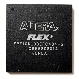
XC6SLX45-2FG484I - 43,661-Cell Spartan-6 FPGA | Xilinx
N.º de pieza: XC6SLX45-2FG484I ✗ Fin de vidaXC6SLX45-2FG484I Descripción general
A field-programmable gate array is a programmable digital integrated circuit whose logic, memory, and signal-processing functions are configured after manufacture. Within the product hierarchy, an FPGA is a semiconductor and reconfigurable digital logic device. The Spartan-6 LX family balances programmable logic capacity with cost-sensitive integration, making devices in this family suitable for embedded control, communications, industrial, medical, and test systems.
Verified listing data identifies 43,661 logic cells, 316 I/O, 500 MHz internal frequency, 45 nm CMOS fabrication, and a 1.2 V supply for this device. It belongs to the Spartan-6 speed-grade portfolio, where the -2 suffix identifies the performance grade and the industrial I suffix identifies the extended-temperature qualification. Other verified details include the 484-BBGA surface-mount package and a lead-free package designation.
The Spartan-6 architecture provides a large fabric of configurable logic and dedicated DSP and memory resources, allowing multiple data-processing paths to execute in parallel. The 316 available I/O support interfaces to external memories, converters, communications transceivers, and control peripherals. The -2 speed grade should be selected when the design requires a balance between processing capability and cost rather than the higher performance offered by a -3 grade.
Typical uses include industrial automation controllers, communications equipment, medical signal-processing systems, network interface controllers, and embedded test platforms. Its 316 I/O are particularly useful for designs requiring multiple external interfaces, while its 43,661 logic cells support parallel datapaths, protocol engines, control logic, and fixed-function accelerator blocks within one programmable device.
The primary design consideration is package and temperature-grade continuity. XC6SLX45-2FG484I must be checked against the exact 484-ball land pattern and the industrial temperature range before substitution. Designers should also validate timing with the appropriate Xilinx timing tools and verify that the selected speed grade satisfies the system clock and I/O requirements without changing the PCB footprint.
This page consolidates verified distributor specifications, same-family drop-in alternatives, application guidance, and design cautions. It distinguishes electrically similar device variants from genuinely interchangeable industrial-temperature replacements and identifies where additional manufacturer documentation is required before a procurement or redesign decision.
Alternativas directas para XC6SLX45-2FG484I — mismo encapsulado, compatible pin a pin. Se excluyen las piezas de otro encapsulado que requieren retrabajo de la PCB.
Variantes de esta serie
Modelos de la misma serie compatibles directamente con XC6SLX45-2FG484I (mismo factor de forma y huella) — difiere en Package, Operating Temperature, Device Type, Package Dimensions, Temperature Grade.
XC6SLX45-2FGG484I
✅ Sustitución directaConsulte el precio
Ver hoja de datos →XC6SLX45-2FG484C
✅ Sustitución directaConsulte el precio
Ver hoja de datos →XC6SLX45-3FG484I
✅ Sustitución directaConsulte el precio
Ver hoja de datos →XC6SLX45-2FGG484C
✅ Sustitución directaConsulte el precio
Ver hoja de datos →XC6SLX45-3FGG484C
✅ Sustitución directaConsulte el precio
Ver hoja de datos →XC6SLX45-2FG484I Valores máximos y características eléctricas
| Device Type | Spartan-6 LX Field Programmable Gate Array (FPGA) |
| Logic Cells | 43,661 cells |
| Number of I/O | 316 I/O |
| Listed Internal Frequency | 500 MHz |
| Process Technology | 45 nm CMOS |
| Core Operating Voltage | 1.2 V |
| Device Family | Spartan-6 LX |
| Speed Grade | -2 |
| Temperature Grade | Industrial |
| Rango de temperatura de funcionamiento | -40°C to +100°C (junction temperature) |
| Encapsulado | 484-BBGA |
| Tipo de montaje | Surface mount |
| Package Pitch | 0.80 mm |
| Package Lead-Free Status | Lead free |
| Number of Logic Cells in Alternative Comparison | 43,661 cells |
Guía de configuración de pines de XC6SLX45-2FG484I lead free
Configuración de pines para XC6SLX45-2FG484I (encapsulado lead free). Este CI digital incluye GPIO, interfaces de comunicación (UART, SPI, I2C) y pines de alimentación. Consulte la hoja de datos del fabricante para conocer las funciones alternativas de los pines y las opciones de configuración. Esencial para el diseño de sistemas embebidos y el diseño de PCB.

No hay datos detallados de patillaje disponibles para XC6SLX45-2FG484I.
Consulte la hoja de datos para ver la configuración completa de patillas.
Aplicaciones típicas
XC6SLX45-2FG484I es adecuado para 6 aplicacións: Industrial Automation and Control, Communications Interface and Protocol Engine, Medical Signal Processing, Network Appliance and Data Preprocessing, Embedded Test and Measurement, Digital Signal Processing Accelerator.
Industrial Automation and Control
The XC6SLX45-2FG484I fits industrial controllers that combine parallel machine-control logic with numerous sensor, actuator, and communications connections. Its 43,661 logic cells provide substantial capacity for motion sequencing, state machines, safety interlocks, and protocol engines, while 316 I/O simplify connection to encoders, I/O modules, analog converters, and field buses. The verified industrial junction-temperature range of -40°C to +100°C is relevant to factory equipment, although the complete enclosure and thermal design determine the final operating margin. The -2 speed grade should be retained when it meets the controller clock requirements, reducing unnecessary timing margin compared with a -3 device.
Recomendado
Communications Interface and Protocol Engine
The XC6SLX45-2FG484I is appropriate for communications equipment requiring parallel packet processing and a high I/O count. The 43,661 logic cells can support framing, routing, filtering, and state-machine workloads, while 316 I/O allow direct connection to transceivers, memories, and network controllers. A 500 MHz listed internal frequency provides ample implementation headroom for parallel datapaths, although external interface rates remain limited by I/O specifications and board-level timing. The -2 grade is the conservative choice when the timing analysis passes; move to a -3 option only if critical paths require the additional performance.
Recomendado
Medical Signal Processing
The XC6SLX45-2FG484I can support parallel medical signal-conditioning and analysis functions where multiple data paths must be processed concurrently. Its 43,661 logic cells are suitable for filtering, feature extraction, timing control, and data acquisition orchestration, while the 316 I/O provide ample connections to sensors, converters, and capture hardware. The industrial temperature suffix is useful for equipment operating across an extended industrial ambient range, but medical-system requirements may demand separate qualification, isolation, and safety validation. The 45 nm CMOS implementation and 1.2 V core supply must also be accounted for in the power architecture and thermal assessment.
Recomendado
Network Appliance and Data Preprocessing
The XC6SLX45-2FG484I is well suited to network appliances that require hardware-assisted packet inspection, buffering, or protocol transformation before data reaches a host processor. Its 43,661 logic cells allow parallel lookup, filtering, and queue-control logic, while 316 I/O can connect multiple memory or communications devices. The listed 500 MHz internal frequency supports high-rate parallel pipelines, but actual network throughput depends on I/O timing, memory architecture, and board constraints. Using the -2 grade where timing closes can reduce procurement and power overhead relative to a -3 device while preserving the same 484-ball mechanical format.
Recomendado
Embedded Test and Measurement
The XC6SLX45-2FG484I can implement parallel test logic, pattern generation, data capture, and instrument-control functions in a compact FPGA-based platform. The 43,661-cell fabric supports timing-intensive state machines and DSP-oriented datapaths, while 316 I/O provide connections to acquisition devices, memory, trigger logic, and communication ports. The listed 500 MHz internal frequency is useful for synchronous pipelines, although instrument timing must be analyzed at the I/O and board level. For a laboratory instrument, the -2 grade can meet many designs, while higher-bandwidth or shorter critical paths may justify evaluating the -3 alternative.
Recomendado
Digital Signal Processing Accelerator
The XC6SLX45-2FG484I is useful when a design needs programmable filtering, correlation, modulation, or other parallel digital signal processing. The 43,661 logic cells can be combined with the Spartan-6 LX DSP resources to implement fixed or parameterized pipelines, while 316 I/O allow direct integration with converters and digital memory. The listed 500 MHz internal frequency provides a basis for high-throughput parallel implementations, but real performance depends on resource sharing, memory bandwidth, and timing closure. The -2 grade should be used when it meets the sample-rate requirement; the -3 grade is an option only for additional timing margin.
Recomendado
Resumen de productos recomendados
Datos de referencia de ingeniería para XC6SLX45-2FG484I — comparación, orientación de diseño e información de cumplimiento.
Guía de selección
Comparación con alternativas
| Parámetro | Este producto | XC6SLX45-2FGG484I | XC6SLX45-2FG484C | XC6SLX45-3FG484I | XC6SLX45-2FGG484C | XC6SLX45-3FGG484C |
|---|---|---|---|---|---|---|
| Package | 484-BBGA | 484-BBGA | 484-BBGA | 484-BBGA | 484-BBGA | 484-BBGA |
| Brand | Xilinx | Xilinx | Xilinx | Xilinx | Xilinx | Xilinx |
| Series | Spartan-6 LX | Spartan-6 LX | Spartan-6 LX | Spartan-6 LX | Spartan-6 LX | Spartan-6 LX |
| Logic Cells | 43,661 cells | 43,661 cells | 43,661 cells | 43,661 cells | 43,661 cells | 43,661 cells |
| Number of I/O | 316 I/O | 316 I/O | 316 I/O | 316 I/O | 316 I/O | 316 I/O |
| Speed Grade | -2 | -2 | -2 | -3 | -2 | -3 |
| Temperature Grade | Industrial, -40°C to +100°C junction | Industrial | Commercial | Industrial | Commercial | Commercial |
| Process Technology | 45 nm CMOS | 45 nm CMOS | 45 nm CMOS | 45 nm CMOS | 45 nm CMOS | 45 nm CMOS |
| Core Operating Voltage | 1.2 V | 1.2 V | 1.2 V | 1.2 V | 1.2 V | 1.2 V |
Diferenciadores clave
- Preserves the original -2 speed grade and industrial temperature class (frente a XC6SLX45-2FGG484C)
- Matches the 43,661-cell and 316-I/O resource configuration (frente a XC6SLX45-3FG484I)
- Avoids the performance and power implication of a -3 upgrade (frente a XC6SLX45-3FGG484C)
Notas de diseño
Do not treat a shared 484-BBGA footprint as sufficient proof of interchangeability. The target uses the -2 speed grade and industrial suffix, while the listed alternatives include -3 speed grades, commercial temperature grades, and G package designations. Before releasing a substitute, compare the complete ordering code, AMD package pinout file, temperature qualification, speed-grade timing models, and power implications. A replacement that passes a distributor cross-reference search can still alter timing closure or environmental suitability.
Budget the 1.2 V core rail and all I/O supplies independently rather than treating the device as a single 1.2 V load. The available excerpts do not provide static or dynamic current tables, so use the current Xilinx power-estimation data for the exact configuration and temperature grade. Include switching activity, clock rate, I/O standards, and accessory utilization in the calculation. Estimated power cannot be derived reliably from the 45 nm process or 500 MHz listed frequency alone because actual FPGA power is configuration-dependent.
Use the official Spartan-6 package pinout file for decoupling, configuration, clock, and I/O ball assignments. Place power and ground connections according to AMD’s package and board-design guidance, and route configuration signals so their state is safe during power-up and reset. The verified excerpts do not provide the complete ball map, so engineers must not infer BGA connectivity from a generic 484-ball drawing. Validate escape routing, via-in-pad or via fanout rules, and solder-assembly capability against the selected PCB process.
Separate clocks, high-speed I/O, and sensitive inputs from noisy power and configuration paths. Apply the I/O timing constraints and board-level budget for every external interface because the device’s listed 500 MHz internal frequency does not guarantee equivalent external signaling performance. For memory or transceiver interfaces, use the manufacturer’s trace-impedance and reference-plane guidance and complete signal-integrity simulation where edge rates are high. These checks are especially important when moving between -2 and -3 alternatives.
Información de cumplimiento
The verified DigChip excerpt explicitly identifies the package as lead free. No explicit RoHS, REACH, halogen-free, conflict-minerals, or AEC-Q100 declaration for the exact ordering code was supplied.