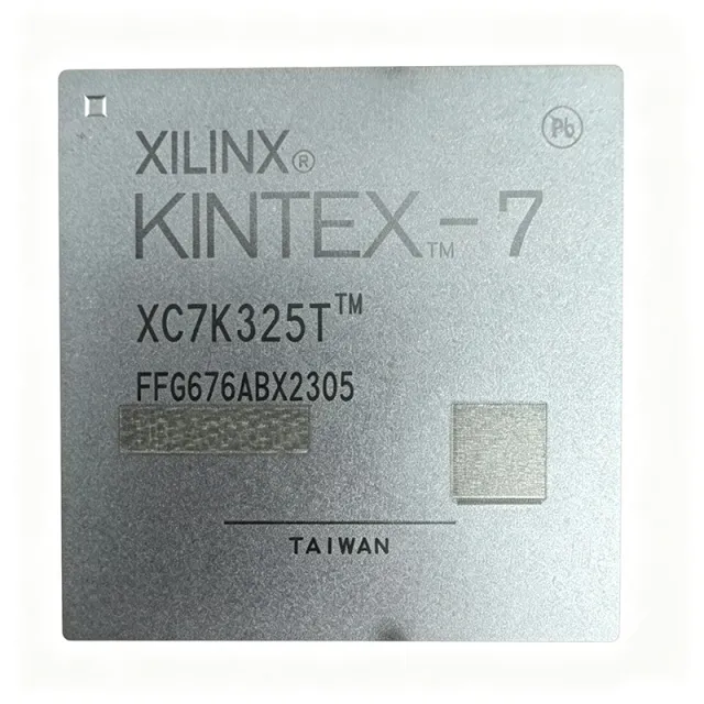
XC7K325T-2FFG676I - Kintex-7 FPGA 326K Logic Cells | AMD
MPN: XC7K325T-2FFG676I ✓ فعال| تعداد | قیمت واحد | قیمت کل |
|---|---|---|
| 1 | $123.63 | $123.63 |
| 10 | $118 | $1,180.00 |
| 100 | $110 | $11,000.00 |
| 500 | $105 | $52,500.00 |
| 1,000 | $98 | $98,000.00 |
XC7K325T-2FFG676I نمای کلی
An FPGA (Field Programmable Gate Array) is an integrated circuit that can be configured by the customer or designer after manufacturing. Unlike fixed-function ASICs, FPGAs contain an array of programmable logic blocks and a hierarchy of reconfigurable interconnects that allow the hardware to be customized to perform specific functions. This flexibility makes FPGAs ideal for prototyping, low-to-mid volume production, and applications requiring hardware acceleration or frequent design updates. The Kintex-7 family sits within the broader FPGA hierarchy, offering a balance between the cost-optimized Artix-7 and the high-performance Virtex-7 families.
Key features of the XC7K325T-2FFG676I include 840 DSP slices for high-throughput digital signal processing, 500 I/O pins (400 user I/Os), and support for a core voltage of 0.97V to 1.03V. The device operates at a maximum frequency of 470.37 MHz and includes advanced clock management tiles (CMTs) with MMCM and PLL for precise clock generation. The -2 speed grade provides a strong balance between performance and power consumption, making it suitable for a wide range of high-speed applications.
Technically, the Kintex-7 architecture integrates a 28nm high-k metal gate (HKMG) process, enabling high logic density and low power. The device includes hardened memory controllers, high-speed transceivers, and PCIe blocks, reducing the need for external components and simplifying system design. The 676-ball FCBGA package offers excellent thermal and electrical performance, supporting the high I/O count and high-speed interfaces required for demanding applications.
Typical applications include software-defined radio, high-performance computing, medical imaging, and aerospace and defense systems. The device's high DSP ratio and support for 10G Ethernet make it particularly well-suited for signal processing and high-throughput data acquisition. Its cost-effective packaging and mainstream standard support also make it a popular choice for communications infrastructure and test and measurement equipment.
When designing with this FPGA, careful attention must be paid to power supply decoupling and thermal management. The core voltage must be maintained within the specified range, and adequate cooling should be provided to keep the junction temperature within limits. The device's configuration interface should be planned early in the design to ensure reliable programming and reconfiguration.
جایگزینهای drop-in برای XC7K325T-2FFG676I — همان پکیج، سازگار پینبهپین. قطعات با پکیج متفاوت که نیاز به تغییر PCB دارند مستثنی هستند.
گونهها در این سری
مدلهای همسری که جایگزین مستقیم هستند برای XC7K325T-2FFG676I (همان فرمفاکتور و فوتپرینت) — متفاوت در Operating Temperature, Mounting Type, RoHS Status.
ابزار مقایسه سریع — قطعات جایگزین را برای مقایسه کنار به کنار انتخاب کنید:
XC7K325T-2FFG676C
📋 جایگزین مرجع (خارج از کاتالوگ)
XC7K325T-1FFG676I
📋 جایگزین مرجع (خارج از کاتالوگ)
XC7K325T-3FFG900E
📋 جایگزین مرجع (خارج از کاتالوگ)
CWC2P300T-FFG676I
📋 جایگزین مرجع (خارج از کاتالوگ)
XC7K325T-2FFG676
📋 جایگزین مرجع (خارج از کاتالوگ)
XC7K325T-2FFG676I حداکثر مقادیر مجاز و مشخصات الکتریکی
| Family | Kintex-7 |
| Number of Logic Elements/Cells | 326080 |
| Number of LABs/CLBs | 25475 |
| Total RAM Bits | 16404480 |
| Number of I/O | 400 |
| Number of DSP Slices | 840 |
| Voltage - Supply | 0.97V ~ 1.03V |
| Maximum Operating Frequency | 470.37 MHz |
| بستهبندی / کیس | 676-BBGA, FCBGA |
| نوع نصب | Surface Mount |
| دمای کاری | -40°C ~ 100°C (TJ) |
| Speed Grade | -2 |
| Number of MMCM/PLL | 10 MMCM, 4 PLL |
| وضعیت RoHS | Compliant |
پیکربندی پین XC7K325T-2FFG676I
| پین A1 | IO_L1P_T0 — User I/O bank 0, differential pair P |
| پین A2 | IO_L1N_T0 — User I/O bank 0, differential pair N |
| پین B1 | VCCINT — Internal core voltage supply (0.97V-1.03V) |
| پین B2 | GND — Ground |
| پین C1 | IO_L2P_T0 — User I/O bank 0, differential pair P |
| پین C2 | IO_L2N_T0 — User I/O bank 0, differential pair N |
| پین D1 | VCCAUX — Auxiliary voltage supply (1.8V) |
| پین D2 | GND — Ground |
| پین E1 | IO_L3P_T0 — User I/O bank 0, differential pair P |
| پین E2 | IO_L3N_T0 — User I/O bank 0, differential pair N |
| پین F1 | VCCIO_0 — I/O bank 0 voltage supply |
| پین F2 | GND — Ground |
کاربردهای معمول
XC7K325T-2FFG676I مناسب است برای 6 کاربردs: Software-Defined Radio, High-Performance Computing, Medical Imaging, Aerospace and Defense, Communications Infrastructure, Test and Measurement.
Software-Defined Radio
The XC7K325T-2FFG676I is ideal for software-defined radio (SDR) due to its 840 DSP slices and high-speed transceivers. It can handle complex modulation and demodulation algorithms, digital down/up conversion, and channel filtering. The device's 400 user I/Os allow for flexible interfacing with ADCs and DACs. Its support for PCIe Gen3 enables high-throughput data transfer to host processors, making it a robust platform for cognitive radio and spectrum monitoring systems.
پیشنهادی
High-Performance Computing
In high-performance computing (HPC), the XC7K325T-2FFG676I accelerates data-intensive workloads such as financial modeling, scientific simulations, and big data analytics. Its 326,080 logic cells and 16.4 Mb of block RAM enable efficient implementation of custom arithmetic units and memory hierarchies. The device's high-speed transceivers support low-latency interconnects like 10G Ethernet, facilitating cluster communication. The -2 speed grade ensures high clock rates for compute-intensive kernels.
پیشنهادی
Medical Imaging
The XC7K325T-2FFG676I is well-suited for medical imaging systems such as ultrasound, CT, and MRI. Its high DSP slice count enables real-time image processing, including filtering, enhancement, and reconstruction. The device's 400 user I/Os allow for direct interfacing with high-speed ADCs and image sensors. The industrial temperature grade ensures reliable operation in clinical environments. Its support for PCIe Gen3 facilitates high-speed data transfer to display and storage systems.
پیشنهادی
Aerospace and Defense
The XC7K325T-2FFG676I is designed for aerospace and defense applications, including radar, electronic warfare, and secure communications. Its industrial temperature range (-40°C to 100°C) ensures operation in harsh environments. The device's high logic density and DSP resources support complex signal processing and beamforming. Its support for 10G Ethernet and PCIe Gen3 enables high-speed data links. The 676-ball FCBGA package provides robust mechanical and thermal performance for mission-critical systems.
پیشنهادی
Communications Infrastructure
The XC7K325T-2FFG676I is a key component in communications infrastructure, including base stations, switches, and routers. Its support for 10G Ethernet and PCIe Gen3 enables high-speed packet processing and forwarding. The device's 326,080 logic cells provide ample resources for implementing protocol stacks and traffic management. The -2 speed grade ensures low-latency operation. Its 400 user I/Os allow for flexible interfacing with PHYs and network processors.
پیشنهادی
Test and Measurement
The XC7K325T-2FFG676I is used in test and measurement equipment such as oscilloscopes, logic analyzers, and signal generators. Its high-speed transceivers and DSP resources enable real-time signal acquisition and analysis. The device's 400 user I/Os allow for direct interfacing with high-speed ADCs and DACs. The industrial temperature grade ensures stable operation in lab environments. Its support for PCIe Gen3 facilitates high-speed data transfer to host computers for visualization and control.
پیشنهادی
خلاصه محصولات پیشنهادی
دادههای مرجع مهندسی برای XC7K325T-2FFG676I — مقایسه، راهنمای طراحی و اطلاعات انطباق.
راهنمای انتخاب
مقایسه با جایگزینها
| پارامتر | این محصول | XC7K325T-2FFG676C | XC7K325T-1FFG676I | XC7K325T-3FFG900E | CWC2P300T-FFG676I |
|---|---|---|---|---|---|
| Package | 676-BBGA, FCBGA | 676-BBGA, FCBGA | 676-BBGA, FCBGA | 900-BBGA, FCBGA | 676-BBGA, FCBGA |
| Brand | AMD | AMD | AMD | AMD | CWC |
تفاوتهای کلیدی
- Industrial temperature grade (در مقابلXC7K325T-2FFG676C)
- Higher speed grade (در مقابلXC7K325T-1FFG676I)
- Pin-compatible with commercial variant (در مقابلXC7K325T-2FFG676C)
یادداشتهای طراحی
The XC7K325T-2FFG676I requires a core voltage of 0.97V to 1.03V. Use a dedicated power management IC to provide a clean, stable supply. Decouple each power pin with a 100nF ceramic capacitor and a 10uF bulk capacitor. Ensure the power supply can handle the device's dynamic current demands, especially during configuration and high-speed operation.
The 676-ball FCBGA package has a thermal resistance that requires careful thermal management. For high-performance applications, use a heatsink and ensure adequate airflow. The junction temperature must not exceed 100°C for the industrial grade. Consider using thermal vias under the package to improve heat dissipation to the PCB ground plane.
For high-speed signals, maintain controlled impedance traces and minimize crosstalk. Use differential pairs for high-speed serial links and ensure proper termination. Place decoupling capacitors close to the FPGA power pins. Follow the layout guidelines in the AMD UG475 for the FCBGA package to ensure reliable operation.
اطلاعات انطباق
RoHS compliant per DigiKey listing. Other compliance data not explicitly provided.
