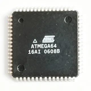
ATMEGA16A-AUR - 8-bit AVR MCU, 16KB Flash, 44-TQFP | Microchip
Référence : ATMEGA16A-AUR ✓ Actif| Qté | Prix unitaire | Total |
|---|---|---|
| 1 | $3.12 | $3,12 |
| 10 | $2.85 | $28,50 |
| 100 | $2.58 | $258,00 |
| 500 | $2.36 | $1 180,00 |
| 1 000 | $2.14 | $2 140,00 |
ATMEGA16A-AUR Présentation
A microcontroller unit (MCU) integrates a processor core, memory, and peripherals on a single silicon die, forming the lowest level of the embedded-system hierarchy: semiconductor -> integrated circuit -> microcontroller -> application-specific embedded controller. The AVR family uses a Harvard architecture with single-cycle instruction execution, allowing throughputs approaching 1 MIPS per MHz so designers can optimize power consumption versus processing speed.
Key features include 133 powerful RISC instructions, most executed in a single clock cycle; 32 x 8-bit general purpose working registers; an 8-channel 10-bit ADC; and an on-chip JTAG interface supporting boundary-scan and on-chip debugging. The device operates from 2.7V to 5.5V, covering both 3.3V and 5V logic systems, and provides three flexible timers/counters with PWM outputs plus a hardware USART for serial communication.
Architecturally, the ATmega16A is a die shrink of the original ATmega16 on a smaller process node, reducing power draw while preserving the pinout and peripheral set. The 16KB self-programmable Flash supports boot-loader based field firmware updates, while the separate 512-byte EEPROM retains calibration data through power cycles.
Typical applications include industrial automation controllers, motor control nodes, sensor data loggers, home appliances, and general-purpose embedded control boards where a 5V-tolerant MCU with integrated ADC and PWM is preferred.
A key design consideration: at 5V the ATmega16A is rated up to 16 MHz, but at 3.3V operation the safe maximum frequency is lower per the datasheet frequency-versus-voltage curve, so clock configuration must match the supply rail.
This page adds value beyond the datasheet by synthesizing distributor pricing tiers, drop-in alternatives, and practical design notes in one place.
Alternatives de remplacement direct pour ATMEGA16A-AUR — même boîtier, compatible broche à broche. Les références à boîtier différent nécessitant une retouche du PCB sont exclues.
Variantes de cette série
Modèles de la même série directement compatibles avec ATMEGA16A-AUR (même facteur de forme et même empreinte) — différant par ADC, Core Architecture, Package, EEPROM, SRAM.
Outil de comparaison rapide — sélectionnez des références alternatives pour une comparaison côte à côte :
ATMEGA16A-AU
✅ Remplacement direct✓ En stock
$2.05 / unité
Voir la fiche technique →ATMEGA32A-AUR
✅ Remplacement direct ⚠️ Spécifications non vérifiées✓ En stock
$2.96 / unité
Voir la fiche technique →ATMEGA162-16AUR
✅ Remplacement direct📋 Alternative de référence (hors catalogue)
ATMEGA8535-16AUR
✅ Remplacement direct ⚠️ Spécifications non vérifiées📋 Alternative de référence (hors catalogue)
ATMEGA16-16AUR
✅ Remplacement direct✓ En stock
$5.98 / unité
Voir la fiche technique →ATMEGA16A-AUR Valeurs maximales et caractéristiques électriques
| Core Architecture | 8-bit AVR RISC |
| Flash Program Memory | 16 KB (8K x 16) |
| SRAM | 1 KB |
| EEPROM | 512 B |
| Fréquence d'horloge maximale | 16 MHz |
| Supply Voltage Range | 2.7 V to 5.5 V |
| Température de fonctionnement | -40C to +85C |
| ADC | 8-channel 10-bit |
| Timers/Counters | 2 x 8-bit, 1 x 16-bit |
| USART | 1 (hardware serial) |
| JTAG Interface | Yes (on-chip debug + boundary scan) |
| Number of I/O | 32 GPIO (4 x 8-bit ports) |
| PWM Channels | 4 |
| Instruction Count | 133 instructions |
| Boîtier | 44-TQFP (10 x 10 mm) |
| Type de montage | Surface Mount |
| Largeur du bus de données | 8 bit |
Configuration des broches de ATMEGA16A-AUR
| Broche 1 | PA7 (ADC7) — Port A bit 7 / ADC channel 7 |
| Broche 2 | PA6 (ADC6) — Port A bit 6 / ADC channel 6 |
| Broche 3 | PA5 (ADC5) — Port A bit 5 / ADC channel 5 |
| Broche 4 | PA4 (ADC4) — Port A bit 4 / ADC channel 4 |
| Broche 5 | PA3 (ADC3) — Port A bit 3 / ADC channel 3 |
| Broche 6 | PA2 (ADC2) — Port A bit 2 / ADC channel 2 |
| Broche 7 | PA1 (ADC1) — Port A bit 1 / ADC channel 1 |
| Broche 8 | PA0 (ADC0) — Port A bit 0 / ADC channel 0 |
| Broche 9 | VCC — Digital supply voltage |
| Broche 10 | GND — Ground |
| Broche 11 | PB7 (SCK) — Port B bit 7 / SPI clock |
| Broche 12 | PB6 (MISO) — Port B bit 6 / SPI data in |
| Broche 13 | PB5 (MOSI) — Port B bit 5 / SPI data out |
| Broche 14 | PB4 (SS) — Port B bit 4 / SPI slave select |
| Broche 15 | PB3 (OC0/AIN1) — Port B bit 3 / Timer0 PWM output / analog comparator input 1 |
| Broche 16 | PB2 (INT2/AIN0) — Port B bit 2 / external interrupt 2 / analog comparator input 0 |
| Broche 17 | PB1 (T1) — Port B bit 1 / Timer1 external clock input |
| Broche 18 | PB0 (T0/XCK) — Port B bit 0 / Timer0 external clock / USART external clock |
| Broche 19 | RESET — Reset input (active low) |
| Broche 20 | VCC — Digital supply voltage |
| Broche 21 | GND — Ground |
| Broche 22 | XTAL2 — Crystal oscillator output 2 |
| Broche 23 | XTAL1 — Crystal oscillator input 1 / external clock input |
| Broche 24 | PD0 (RXD) — Port D bit 0 / USART receive |
| Broche 25 | PD1 (TXD) — Port D bit 1 / USART transmit |
| Broche 26 | PD2 (INT0) — Port D bit 2 / external interrupt 0 |
| Broche 27 | PD3 (INT1) — Port D bit 3 / external interrupt 1 |
| Broche 28 | PD4 (OC1B) — Port D bit 4 / Timer1 output compare B (PWM) |
| Broche 29 | PD5 (OC1A) — Port D bit 5 / Timer1 output compare A (PWM) |
| Broche 30 | PD6 (ICP1) — Port D bit 6 / Timer1 input capture |
| Broche 31 | PD7 (OC2) — Port D bit 7 / Timer2 output compare (PWM) |
| Broche 32 | VCC — Digital supply voltage |
| Broche 33 | GND — Ground |
| Broche 34 | PC0 (SCL) — Port C bit 0 / TWI clock |
| Broche 35 | PC1 (SDA) — Port C bit 1 / TWI data |
| Broche 36 | PC2 (TCK) — Port C bit 2 / JTAG test clock |
| Broche 37 | PC3 (TMS) — Port C bit 3 / JTAG test mode select |
| Broche 38 | PC4 (TDO) — Port C bit 4 / JTAG test data out |
| Broche 39 | PC5 (TDI) — Port C bit 5 / JTAG test data in |
| Broche 40 | PC6 (TOSC1) — Port C bit 6 / Timer oscillator input 1 |
| Broche 41 | PC7 (TOSC2) — Port C bit 7 / Timer oscillator output 2 |
| Broche 42 | AVCC — ADC supply voltage (connect to VCC via low-pass filter) |
| Broche 43 | AREF — ADC analog reference input |
| Broche 44 | AGND — Analog ground |
Applications typiques
ATMEGA16A-AUR convient pour 6 applications: Industrial Automation Controllers, Motor Control and PWM Drivers, Sensor Data Acquisition Nodes, Home Appliances and White Goods, Legacy AVR Design Maintenance, Security and Access Control Systems.
Industrial Automation Controllers
The ATMEGA16A-AUR suits industrial control nodes because its 8-channel 10-bit ADC digitizes multiple sensor inputs (temperature, potentiometer setpoints, current shunts) while four PWM channels drive actuators or heater control elements. Its 5V supply range and -40C to +85C rating tolerate factory-floor electrical noise and temperature swings, and the 16KB Flash accommodates Modbus or custom protocol stacks with headroom. Placed as the local controller between field sensors and relays, the 16 MHz AVR core achieves roughly 16 MIPS, sufficient for 1 ms control loops. The on-chip JTAG interface enables in-target debugging during commissioning without additional debug chips, and the 512B EEPROM stores calibration constants that survive power interruptions.
Recommandé
Motor Control and PWM Drivers
With one 16-bit timer and two 8-bit timers delivering four PWM channels, the ATMEGA16A-AUR directly generates speed-control PWM for DC motors, servo positioning pulses, and BLDC commutation schemes in small drives. The 16 MHz clock provides PWM resolutions up to 16-bit at low frequencies or fast 20 kHz switching with 10-bit resolution for quiet fan and pump control. ADC feedback reads current-sense shunts via the 10-bit converter for closed-loop torque limiting. Operating from 5V, its GPIO can interface through MOSFET gate drivers; at 16 MHz the core completes control-loop math within microseconds, and the external interrupt pins (INT0/INT1/INT2) capture encoder pulses for position feedback.
Recommandé
Sensor Data Acquisition Nodes
The 8-channel 10-bit ADC with an internal reference and differential input capability makes the ATMEGA16A-AUR a compact front end for multi-sensor acquisition nodes. Analog inputs on Port A scan thermistors, humidity elements, and pressure bridges; the hardware USART streams readings over RS-485 or RS-232 links at standard baud rates derived from the 16 MHz clock. The 512B EEPROM holds sensor offset tables and device IDs, while 1KB SRAM buffers rolling-window data for filtering. Successive-approximation conversion times of roughly 13 ADC clock cycles allow tens of thousands of samples per second - ample for environmental monitoring where minute-level logging and local threshold alarms are the primary workload.
Recommandé
Home Appliances and White Goods
Consumer appliances benefit from the ATMEGA16A-AUR's combination of robust 5V operation, PWM-driven heater or motor control, and low-cost BOM position. Buttons and encoder inputs map naturally onto the 32 GPIO lines across four 8-bit ports, LED and seven-segment displays are driven directly from spare pins, and the 16KB Flash stores both control logic and UI behavior without external memory. Its -40C to +85C automotive-style temperature range covers kitchen and laundry environments, and the watchdog timer plus brown-out detector deliver the fault recovery expected in mains-powered products. Wide 2.7V-5.5V supply tolerance also simplifies designs powered by unregulated wall-transformer DC.
Recommandé
Legacy AVR Design Maintenance
The ATMEGA16A-AUR is the designated active-production replacement for boards designed around the original ATmega16: per Microchip application note AVR522, the ATmega16A is a functionally identical drop-in replacement passing the same qualification and production tests. Engineers maintaining industrial controllers, instrumentation, or robotics designed in the 2000s can reflow the ATMEGA16A-AUR onto the existing TQFP-44 footprint without PCB or firmware changes, though minor electrical differences from the new process should be reviewed in the current datasheet. This makes it the standard choice for end-of-life mitigation, keeping certified legacy products in production without requalification.
Recommandé
Security and Access Control Systems
Access-control panels use the ATMEGA16A-AUR to scan keypad matrices on Port B/C, drive door-strike relays through PWM-timed GPIO, and communicate events over the USART to a central controller. The JTAG interface on Port C doubles as a boundary-scan resource for production board testing, while the EEPROM stores user codes and event logs across power cycles. At 16 MHz the AVR executes authentication and encryption routines fast enough for sub-100 ms card-read response, and the brown-out detector prevents EEPROM corruption during brownouts. The wide 2.7V-5.5V input range supports battery-backup operation when mains power fails, a requirement in security installations.
Recommandé
Récapitulatif des produits recommandés
Données de référence d'ingénierie pour ATMEGA16A-AUR — comparaison, recommandations de conception et informations de conformité.
Guide de sélection
Comparaison avec les alternatives
| Paramètre | Ce produit | ATMEGA16A-AU | ATMEGA32A-AUR | ATMEGA162-16AUR | ATMEGA8535-16AUR |
|---|---|---|---|---|---|
| Brand | Microchip Technology | Microchip Technology | Microchip Technology | Microchip Technology | Microchip Technology |
| Package | 44-TQFP (10x10) | 44-TQFP (10x10) - same | 44-TQFP (10x10) - same | 44-TQFP (10x10) - same | 44-TQFP (10x10) - same |
| Flash Memory | 16 KB | 16 KB | 32 KB | 16 KB | 8 KB |
| SRAM | 1 KB | 1 KB | 2 KB | 1 KB | 512 B |
| Max Clock Frequency | 16 MHz | 16 MHz | 16 MHz | 16 MHz | 16 MHz |
| USART Count | 1 | 1 | 1 | 2 | 1 |
| Packaging | Tape & Reel | Tray | Tape & Reel | Tape & Reel | Tape & Reel |
Principaux différenciateurs
- Lowest-cost entry point with JTAG debug (vs ATMEGA32A-AUR)
- Active-production replacement for legacy ATmega16 (vs ATMEGA16-16AUR)
- Larger memory vs. smaller-footprint family members (vs ATMEGA8535-16AUR)
Notes de conception
Decouple all three VCC pins (9, 20, 32) plus AVCC (pin 42) with 100 nF ceramic capacitors placed within 5 mm of each pin, plus one bulk 10 uF per supply rail. AVCC should be connected to VCC through a low-pass RC network (e.g. 10 ohm / 100 nF) when ADC accuracy matters - Microchip's datasheet notes AVCC must stay within 0.3V of VCC. The brown-out detector should be enabled via fuse for reliable EEPROM writes during supply sag.
Keep the crystal traces from XTAL1/XTAL2 (pins 23/22) short and guard them with ground pour to avoid stray pickup; load capacitors should match the 16 MHz crystal spec, typically 22 pF. Route the analog Port A ADC traces away from PWM outputs on Port D (OC1A/OC1B/OC2) to prevent switching noise coupling into conversions. Use a solid ground plane and connect AGND (pin 44) to it at a single quiet point for best ADC performance.
The most frequent ATmega16 design error is running 16 MHz at 3.3V: the datasheet frequency-vs-voltage curve limits maximum clock at reduced VCC, causing marginal-timing failures that appear only over temperature. Second, fuse-bit misconfiguration (disabling SPIEN or enabling the wrong clock source) can brick the part in-circuit; recovery requires high-voltage parallel programming. Third, if migrating from the original ATmega16, review AVR522 for electrical characteristic changes on the new die process before requalification.
Informations de conformité
Distributor listings categorize ATMEGA16A-AUR as RoHS Compliant; PartGenie data confirms RoHS compliance. REACH and conflict-minerals declarations not present in provided data.