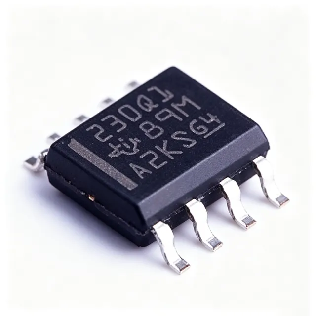
SN65HVD230QDRQ1 - 3.3V CAN Transceiver AEC-Q100 | Texas Instruments
Référence : SN65HVD230QDRQ1 ✓ Actif| Qté | Prix unitaire | Total |
|---|---|---|
| 1 | $1.69 | $1,69 |
| 10 | $1.53 | $15,30 |
| 100 | $1.3853 | $138,53 |
| 500 | $1.24 | $620,00 |
| 1 000 | $1.11 | $1 110,00 |
SN65HVD230QDRQ1 Présentation
A controller area network (CAN) transceiver is a physical-layer interface IC that converts the logic-level TXD and RXD signals of a CAN controller into the differential CANH and CANL bus signals defined by the ISO 11898-2 High Speed CAN Physical Layer standard. Within the interface IC hierarchy, it sits between the protocol controller and the twisted-pair bus, providing driver, receiver, ESD protection, and fault-tolerance functions for the network node.
Key features include ISO 11898-2 compatibility, a low-current standby mode drawing approximately 370 uA typical, bus-pin ESD protection exceeding 15 kV HBM (exceeding 2000 V per MIL-STD-883 on the device), controlled driver output transition times for improved signal quality, and a dominant-timeout feature. An unpowered node does not disturb the bus, and the RS pin selects slew-rate control or low-power mode.
The SN65HVD230Q family (SN65HVD230Q, SN65HVD231Q, SN65HVD232Q) was designed to pair directly with TI TMS320Lx240x 3.3-V DSPs with on-chip CAN controllers, and also serves as a low-power replacement for the classic PCA82C250 footprint. Operating from a single 3.3-V rail eliminates level shifting when the host MCU or DSP is a 3.3-V device, reducing BOM count and board area in automotive body electronics, gateway modules, and industrial CAN nodes.
Typical applications include automotive body control modules, battery management systems with 3.3-V MCUs, industrial 3.3-V CAN networks, and building automation nodes where a 5-V supply is unavailable.
Design consideration: the RS pin mode selection determines standby and sleep behavior - drive or tie it so the node can wake the transceiver from its 370 uA standby state when bus activity resumes, and provide a 4.7 kOhm to 10 kOhm split-termination network on CANH/CANL per ISO 11898-2 layout practice.
This page synthesizes verified distributor pricing, same-package drop-in alternatives, and practical design notes not found in the manufacturer datasheet.
Alternatives de remplacement direct pour SN65HVD230QDRQ1 — même boîtier, compatible broche à broche. Les références à boîtier différent nécessitant une retouche du PCB sont exclues.
Variantes de cette série
Modèles de la même série directement compatibles avec SN65HVD230QDRQ1 (même facteur de forme et même empreinte) — différant par Package, Data Rate, Protocol, Supply Voltage, Function.
Outil de comparaison rapide — sélectionnez des références alternatives pour une comparaison côte à côte :
SN65HVD230DR
✅ Remplacement direct✓ En stock
$0.94 / unité
Voir la fiche technique →SN65HVD230QDR
✅ Remplacement direct📋 Alternative de référence (hors catalogue)
SN65HVD231QDRQ1
✅ Remplacement direct ⚠️ Spécifications non vérifiées📋 Alternative de référence (hors catalogue)
SN65HVD232QDRQ1
✅ Remplacement direct📋 Alternative de référence (hors catalogue)
TCAN337G
✅ Remplacement direct✓ En stock
$0.55 / unité
Voir la fiche technique →TJA1051T/3/1
✅ Remplacement direct✓ En stock
$0.4102 / unité
Voir la fiche technique →SN65HVD230QDRQ1 Spécifications
| Transceiver Type | CAN (Half-duplex, 1 driver / 1 receiver) |
| Débit de données | Up to 1 Mbps |
| Tension d'alimentation | 3.3 V |
| Standby Mode Current | 370 uA (typical) |
| Bus Pin ESD Protection | Exceeds 15 kV HBM |
| Device ESD Rating | Exceeds 2000 V per MIL-STD-883 |
| Protocol Compatibility | ISO 11898-2 High Speed CAN Physical Layer |
| Standby Mode | Yes (RS pin controlled) |
| Dominant Timeout | Yes |
| Slew Rate Control | Yes (RS pin) |
| Unpowered Node Behavior | Does not disturb the bus |
| Plage de température de fonctionnement | -40C to +125C |
| AEC-Q100 Qualification | Qualified (Automotive Catalog) |
| Boîtier | 8-SOIC (D), 3.90 mm width |
| Type de montage | Surface Mount |
| Packaging | Tape & Reel (DR) |
Configuration des broches de SN65HVD230QDRQ1
| Broche 1 | D (TXD) — Driver input from CAN controller transmit data |
| Broche 2 | GND — Ground |
| Broche 3 | VCC — 3.3-V supply voltage |
| Broche 4 | R (RXD) — Receiver output to CAN controller receive data |
| Broche 5 | VREF — Reference output voltage |
| Broche 6 | CANL — Low-level CAN bus line |
| Broche 7 | CANH — High-level CAN bus line |
| Broche 8 | RS — Mode selection: slope control, high-speed, standby, or sleep |
Applications typiques
SN65HVD230QDRQ1 convient pour 6 applications: Automotive Body Electronics, Automotive Gateway Modules, Battery Management Systems (3.3V), Industrial CAN Networks, Low-Power Battery-Fed CAN Nodes, Legacy PCA82C250 Footprint Migration.
Automotive Body Electronics
The SN65HVD230QDRQ1 is AEC-Q100 qualified and rated -40C to +125C, making it a direct fit for automotive body control modules, door modules, lighting controllers, and seat-control nodes that run 3.3-V MCUs. Its ISO 11898-2 compatibility guarantees interoperability with the vehicle high-speed CAN bus at up to 1 Mbps, while bus-pin ESD protection exceeding 15 kV HBM withstands the harsh electrical environment of vehicle harnesses. In body nodes that sleep for long periods, the RS-pin standby mode cuts transceiver consumption to approximately 370 uA typical, preserving battery budget. Place the device close to the connector with a 100 nF local decoupling capacitor and route CANH/CANL as a tightly coupled differential pair. Per the TI datasheet, an unpowered node does not disturb the bus, improving network robustness during module faults.
Recommandé
Automotive Gateway Modules
Gateway modules bridge multiple CAN channels and require transceivers with proven automotive qualification and predictable bus behavior. The SN65HVD230QDRQ1's controlled driver output transition times improve signal quality on long harness segments, reducing ringing and electromagnetic emissions at 1 Mbps. The dominant-timeout feature prevents a hung controller TXD from blocking the entire bus, a key safety consideration in gateways that fan out traffic across networks. Because the gateway MCU typically runs from a 3.3-V rail, the 3.3-V transceiver supply eliminates level-shift circuitry and its associated delay. TI supports customer-specific configuration control along with major-change approval, easing PPAP-style change management for Tier-1 builds. Combined with an unpowered-node non-disturbing bus characteristic, the device keeps partial gateway failures from taking down the whole network.
Recommandé
Battery Management Systems (3.3V)
Battery management systems built on 3.3-V MCUs (or DSPs like the TMS320Lx240x family this part was designed for) benefit directly from the SN65HVD230QDRQ1's native 3.3-V operation, which removes level shifters between the CAN controller and the bus. The low 370 uA standby current matters in battery-powered or always-on monitoring nodes, and the RS-pin slew-rate control lets the designer trade edge speed for EMC margin near sensitive cell-measurement front ends. ESD robustness above 15 kV HBM on CANH/CANL helps survive pack assembly and service handling. Note the trade-off: a 3.3-V transceiver provides less differential output swing margin on heavily loaded or long bus runs than a 5-V part, so verify loop delay and termination resistance across the full pack temperature range before committing the layout.
Recommandé
Industrial CAN Networks
In factory automation, motor-drive control, and building automation, 3.3-V CAN networks are increasingly common as controllers migrate from 5-V to 3.3-V silicon. The SN65HVD230QDRQ1 meets ISO 11898-2 at 1 Mbps for the high-speed physical layer these networks require, and its controlled transition times reduce radiated emissions on cable trays and bus bars. The standby mode suits periodically-woken sensor and actuator nodes, dropping supply current to approximately 370 uA when idle. Its unpowered-node bus behavior allows hot-plugging of nodes on a live network without corrupting frames - a practical benefit in modular industrial systems. For electrically noisy environments or long cable runs, pair the transceiver with proper split termination (two resistors of 60-66 Ohm each with a 2.2-4.7 nF capacitor to ground) and twisted-pair cabling per standard practice.
Recommandé
Low-Power Battery-Fed CAN Nodes
Remote telemetry units, wireless-tethered sensors, and periodically-woken actuators live or die by average current draw. Here the SN65HVD230QDRQ1's headline feature is the 370 uA typical standby mode, controllable by the host MCU through the RS pin. The sleep state persists until the RS pin is reactivated with a low logic level, letting a supervisor or RTC schedule wake windows around bus activity. Because the transceiver shares the 3.3-V rail with the MCU, no second regulator is needed, cutting quiescent budget further. Design carefully around wake latency: the node must allow time for the transceiver to exit standby before the first frame is transmitted, typically by scheduling a wake period ahead of the expected bus message. Verify recessive bus biasing in standby so the node does not split the differential bus voltage while sleeping.
Recommandé
Legacy PCA82C250 Footprint Migration
Many legacy industrial and automotive boards were designed around the 5-V Philips/NXP PCA82C250 CAN transceiver, now obsolete or cost-prohibitive. TI explicitly positions the SN65HVD230Q family as a low-power replacement for the PCA82C250 footprint, allowing designers to refresh the bill of materials while keeping the same 8-pin SOIC layout intent. The migration cuts quiescent power substantially through the 370 uA standby mode and permits consolidation on a 3.3-V rail when the controller is also 3.3 V. Before dropping in, audit three areas: supply rail availability (3.3 V must be present and clean), recessive bias differences versus the 5-V original, and RS pin termination, which the PCA82C250 did not have. TI's datasheet typical application section provides the recommended RS mode resistor values for slope control at various bit rates.
Recommandé
Récapitulatif des produits recommandés
Données de référence d'ingénierie pour SN65HVD230QDRQ1 — comparaison, recommandations de conception et informations de conformité.
Guide de sélection
Comparaison avec les alternatives
| Paramètre | Ce produit | SN65HVD230DR | SN65HVD230QDR | SN65HVD231QDRQ1 | SN65HVD232QDRQ1 | TCAN337G | TJA1051T/3/1 |
|---|---|---|---|---|---|---|---|
| Package | 8-SOIC (D) | 8-SOIC (D) - same | 8-SOIC (D) - same | 8-SOIC (D) - same | 8-SOIC (D) - same | 8-SOIC (D) - same | 8-SOIC (D) - same |
| Brand | Texas Instruments | Texas Instruments | Texas Instruments | Texas Instruments | Texas Instruments | Texas Instruments | NXP Semiconductors |
| Supply Voltage | 3.3 V | 3.3 V | 3.3 V | 3.3 V | 3.3 V | 3.3 V | 5 V core / VIO 3.3 V |
| Data Rate | 1 Mbps | 1 Mbps | 1 Mbps | 1 Mbps | 1 Mbps | 1 Mbps / CAN FD tolerant | 1 Mbps (5 Mbps pin-selected up to 500 kbps default) |
| Standby Mode | Yes (370 uA typical) | Yes (370 uA typical) | Yes (370 uA typical) | Yes (with wake-up) | No | No standby; low-power modes differ | No |
| Pin 5 Function | VREF | VREF | VREF | VREF | NC / VREF-related | WAKE / auxiliary (verify per datasheet) | VIO (3.3 V logic supply) |
Principaux différenciateurs
- Lowest-power idle state in the family (vs SN65HVD232QDRQ1)
- Automotive change-control support (vs SN65HVD230DR)
- Genuine 3.3-V single-supply operation (vs TJA1051T/3/1)
- Modern upgrade path exists without footprint change (vs TCAN337G)
Notes de conception
Place a 100 nF ceramic decoupling capacitor within 3 mm of the VCC pin (pin 3) with a solid via to the ground plane. Route CANH (pin 7) and CANL (pin 6) as a tightly coupled differential pair with matched lengths, exiting the board toward the bus connector without crossing high-di/dt switching nets. Use a split termination (two 60-66 Ohm resistors with 2.2-4.7 nF to GND) at the two physical bus ends. Keep the RS pin (pin 8) trace short; a grounding resistor here sets the slew rate for EMC per TI datasheet guidance.
The RS pin governs mode: leaving it floating can produce undefined standby/sleep behavior and a silent node. Drive it deliberately - ground for high-speed, resistor for slope control, high level for 370 uA standby. Also remember the dominant-timeout feature limits how long a stuck TXD can hold the bus dominant; do not disable your controller watchdog assuming the transceiver alone guarantees recovery. Finally, when migrating from a 5-V PCA82C250, confirm your 3.3-V rail is present before bus frames are exchanged, since the recessive bias changes.
At 1 Mbps the bit time is 1 us, so loop delay (controller plus transceiver plus cable) must remain well inside the ISO 11898-2 budget. The SN65HVD230Q's controlled transition times trade edge speed for lower ringing and emissions - beneficial on unshielded harnesses, but at long cable lengths verify propagation delay across temperature (-40C to +125C) using the datasheet typical curves. Add a small common-mode choke (e.g., 51 uH dual-winding class) at the connector if the vehicle or factory EMC specification demands it.
Estimated: standby consumption of 370 uA (datasheet typical) at 3.3 V yields about 1.2 mW, negligible versus a battery's self-discharge; active dominant loading dominated by termination current is roughly 60 mA into 60 Ohm effective load (Estimated: 3.3 V / 60 Ohm approximately 55 mA, most of it dissipated in the external termination, not the IC). Budget the 3.3-V regulator for the dominant-state current of every simultaneously transmitting node if the local supply also feeds termination resistors.
Informations de conformité
AEC-Q100 qualification confirmed in TI datasheet (Automotive Catalog). RoHS/lead-free assumed from TI current-production status for DR suffix; REACH, halogen-free, and conflict-minerals status must be confirmed on the TI quality portal for the specific date code.







