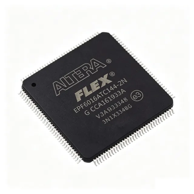
EPF6016ATC144-2
EPF6016ATC144-2 - FLEX 6000 FPGA, 16K Gates, 117 I/O | Intel
The Intel (formerly Altera) EPF6016ATC144-2 is a member of the FLEX 6000 family of SRAM-based reprogrammable FPGAs, delivering 16,000 typical gates (24,000 maximum logic elements) in a 144-pin LQFP (LFQFP) surface-mount package with 117 user I/Os. Built on a 0.30 µm CMOS SRAM process, the device combines 1,320 logic elements organized into 132 Logic Array Blocks (LABs), each containing 10 LEs connected by carry and cascade chains for high-speed arithmetic and wide-input functions.
What is an FPGA? A Field-Programmable Gate Array (FPGA) is a semiconductor IC containing a matrix of configurable logic blocks (CLBs), programmable interconnect, and I/O cells, all defined by a user-supplied bitstream after manufacturing. FPGAs sit between fixed-function ASICs and software-driven processors in the digital-design hierarchy, offering hardware-timed parallelism, fast time-to-prototype, and field re-programmability for design iteration, algorithm acceleration, and glue-logic integration. The FLEX 6000 family targets low-to-mid density glue logic and is part of the broader programmable logic device (PLD) taxonomy.
Key features of the EPF6016ATC144-2 include 117 user I/Os, 132 LABs, on-chip SRAM-based configuration memory, in-system programmability via JTAG (IEEE 1149.1), and support for Altera MAX+PLUS II and Quartus design flows. The device operates from a single supply voltage and supports the commercial temperature grade. Carry chains support high-speed arithmetic functions such as counters and adders, while cascade chains implement wide-input functions with minimum delay. Dedicated clock pins and global routing enable deterministic timing for synchronous designs.
The EPF6010/EPF6016 family uses the OptiFLEX architecture with continuous horizontal routing across rows and vertical routing in columns, balancing density and routability for designs up to ~16K gates. The architecture supports LPM, VHDL, Verilog HDL, and EDIF 2.0/3.0 design entry, allowing seamless integration with third-party EDA synthesis and simulation tools. Internal configuration memory is volatile and must be loaded from an external serial or parallel PROM at power-up, or via JTAG.
Typical applications for the EPF6016ATC144-2 include glue logic for industrial control boards, I/O expansion and bus interfacing, prototyping of mid-density digital designs, replacement of discrete TTL/CMOS logic, custom peripheral controllers in embedded systems, and educational platforms teaching FPGA design with MAX+PLUS II. The 117 I/Os make it suitable for designs with moderate I/O count, while the 144-pin LQFP package simplifies PCB assembly with standard surface-mount equipment.
When designing with this device, consider that configuration memory is volatile - a serial configuration EPROM (e.g., EPC2, EPC4) is required to load the bitstream on power-up, or JTAG can be used for prototype programming. The 144-pin LQFP package has a 0.5 mm pin pitch and requires careful PCB layout for signal integrity. Decoupling capacitors (0.1 µF and 10 µF) should be placed adjacent to every supply pin to minimize switching noise.
This page synthesizes distributor pricing, lifecycle data, drop-in package-compatible alternatives from the FLEX 6000/10K family, and practical design notes not found in the manufacturer datasheet alone, helping engineers select the right pin-compatible FPGA for legacy or new designs.
USD $13,85
Kontak