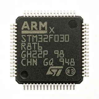
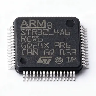
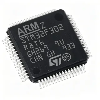
STM32F103RBT6 - 72MHz Cortex-M3 MCU 128KB Flash | ST
MPN: STM32F103RBT6 ✓ AktifSTM32F103RBT6 Ringkasan
A microcontroller unit (MCU) is a single integrated circuit that combines a processor core, memory, and programmable peripherals into one device, forming the lowest layer of the embedded-system hierarchy: MCU -> microcontroller -> embedded processor -> system-on-chip. The ARM Cortex-M3 is a 32-bit RISC processor core optimized for cost-sensitive and power-conscious embedded control. The STM32F103 family was one of the first mainstream Cortex-M families adopted at scale across industrial electronics, in large part because of its rich peripheral set and pin compatibility across Flash derivatives.
Key features include the 72 MHz Cortex-M3 core delivering 1.25 DMIPS/MHz, 128 KB on-chip Flash, 20 KB SRAM, a 2.0 V to 3.6 V supply range with a 3.3 V operating point, two 12-bit ADCs with up to 1 microsecond conversion time and up to 16 input channels, two I2C, two SPI, three USART, one USB 2.0 full-speed interface, one CAN 2.0B active controller, and seven 16-bit timers including PWM-capable channels. An 8 MHz high-speed internal RC oscillator and support for an external 4 to 16 MHz crystal allow flexible clocking without external components.
Architecturally, the device uses an ARMv7-M Harvard structure with a three-stage pipeline and a Nested Vectored Interrupt Controller (NVIC) for low-latency interrupt response. An AHB/APB bus matrix allows peripheral DMA and core execution to proceed concurrently, while a Flash interface with prefetch buffer minimizes stalls when the 72 MHz core fetches instructions from Flash.
Typical applications include industrial control nodes, motor-control auxiliary boards, USB and CAN communication modules, low-cost development platforms, and legacy 8-bit/16-bit MCU upgrades where the ARM tool ecosystem reduces software cost. Designers also use this device in smart-metering peripherals and low-cost HMIs.
Design consideration: pin compatibility across the STM32F1 family means Flash upgrades from 128 KB to 256 KB (e.g., STM32F103RCT6) require no PCB change, but verify RAM sizing, peripheral count, and the 72 MHz maximum frequency when porting between derivative families.
This page synthesizes distributor pricing, verified drop-in alternatives including the GD32F103RBT6 cross-brand P2P candidate and STM32F103RCT6 same-family upgrade, plus practical design notes not found in the manufacturer datasheet.
Alternatif penggantian untuk STM32F103RBT6 — paket yang sama, pin-pada-pin kompatibel. Bagian paket yang berbeda memerlukan kerja ulang PCB diabaikan.
Variasi di dalam seri ini
Model-series yang sama yang kompatibel dengan penggantian STM32F103RBT6 (sama faktor bentuk dan footprint) — berbeda di dalam Package, Timers, Flash Memory, ADC, Operating Temperature.
STM32F103RCT6
✅ Drop-InKontak untuk harga
Lihat Datasheet →STM32F103R8T6
✅ Drop-InKontak untuk harga
Lihat Datasheet →GD32F103RBT6
✅ Drop-In📋 Alternatif referensi (tidak dalam katalog)
APM32F103RBT6
✅ Drop-In📋 Alternatif referensi (tidak dalam katalog)
STM32F103RBT6 Rating Maksimal & Karakteristik Listrik
| Core | ARM Cortex-M3 32-bit RISC |
| Frekuensi Bawah Maximum | 72 MHz |
| Core Performance | 1.25 DMIPS/MHz |
| Program Memory (Flash) | 128 KB |
| SRAM | 20 KB |
| Supply Voltage (VDD) | 2.0 V to 3.6 V |
| Suhu Kerja | -40 C to +85 C (industrial grade) |
| Paket | LQFP-64 (10x10 mm) |
| Tipe Mounting | Surface Mount |
| ADC | 2 x 12-bit, 1 us conversion, up to 16 channels |
| Timers | 7 x 16-bit (including PWM) |
| Communication Interfaces | 2 x SPI, 2 x I2C, 3 x USART, 1 x USB 2.0 FS, 1 x CAN 2.0B |
| I/O Pins (approx.) | 51 GPIOs |
| Internal Oscillator | 8 MHz HSI RC |
| External Crystal Range | 4 MHz to 16 MHz |
| DMA Channels | 7 channels |
| Level MSL | 3 (per JEDEC J-STD-020) |
| Status RoHS | Compliant |
Konfigurasi Pin STM32F103RBT6
| Pin produk 1 | VBAT — RTC backup supply |
| Pin produk 2 | PC13/TAMPER-RTC — GPIO PC13 or RTC tamper input |
| Pin produk 3 | PC14/OSC32_IN — GPIO PC14 or 32 kHz crystal in |
| Pin produk 4 | PC15/OSC32_OUT — GPIO PC15 or 32 kHz crystal out |
| Pin produk 5 | OSC_IN — External clock input / crystal in |
| Pin produk 6 | OSC_OUT — External clock output / crystal out |
| Pin produk 7 | NRST — Reset input (active low) |
| Pin produk 8 | VSSA — Analog ground |
| Pin produk 9 | VDDA — Analog supply (3.3 V) |
| Pin produk 10 | PA0/WKUP — GPIO PA0 / wakeup / ADC_IN0 |
| Pin produk 11 | PA1 — GPIO PA1 / ADC_IN1 |
| Pin produk 12 | PA2 — GPIO PA2 / USART2_TX / ADC_IN2 |
| Pin produk 13 | PA3 — GPIO PA3 / USART2_RX / ADC_IN3 |
| Pin produk 14 | PA4 — GPIO PA4 / SPI1_NSS / ADC_IN4 |
| Pin produk 15 | PA5 — GPIO PA5 / SPI1_SCK / ADC_IN5 |
| Pin produk 16 | PA6 — GPIO PA6 / SPI1_MISO / ADC_IN6 |
| Pin produk 17 | PA7 — GPIO PA7 / SPI1_MOSI / ADC_IN7 |
| Pin produk 18 | PB0 — GPIO PB0 / ADC_IN8 |
| Pin produk 19 | PB1 — GPIO PB1 / ADC_IN9 |
| Pin produk 20 | PB2/BOOT1 — GPIO PB2 / boot mode select |
| Pin produk 21 | PB10 — GPIO PB10 / I2C2_SCL / USART3_TX |
| Pin produk 22 | PB11 — GPIO PB11 / I2C2_SDA / USART3_RX |
| Pin produk 23 | VSS_1 — Ground |
| Pin produk 24 | VDD_1 — Digital supply (3.3 V) |
| Pin produk 25 | PB12 — GPIO PB12 / SPI2_NSS |
| Pin produk 26 | PB13 — GPIO PB13 / SPI2_SCK |
| Pin produk 27 | PB14 — GPIO PB14 / SPI2_MISO |
| Pin produk 28 | PB15 — GPIO PB15 / SPI2_MOSI |
| Pin produk 29 | PA8 — GPIO PA8 / USART1_CK / TIM1_CH1 |
| Pin produk 30 | PA9 — GPIO PA9 / USART1_TX / TIM1_CH2 |
| Pin produk 31 | PA10 — GPIO PA10 / USART1_RX / TIM1_CH3 |
| Pin produk 32 | PA11/USBDM — GPIO PA11 / USB D- |
| Pin produk 33 | PA12/USBDP — GPIO PA12 / USB D+ |
| Pin produk 34 | PA13/SWDIO — GPIO PA13 / SWD data |
| Pin produk 35 | VSS_2 — Ground |
| Pin produk 36 | VDD_2 — Digital supply (3.3 V) |
| Pin produk 37 | PA14/SWCLK — GPIO PA14 / SWD clock |
| Pin produk 38 | PA15 — GPIO PA15 / TIM2_CH1_ETR / SPI1_NSS_remap |
| Pin produk 39 | PB3 — GPIO PB3 / TIM2_CH2 / SPI1_SCK_remap |
| Pin produk 40 | PB4 — GPIO PB4 / TIM3_CH1 / SPI1_MISO_remap |
| Pin produk 41 | PB5 — GPIO PB5 / I2C1_SMBAI / TIM3_CH2 |
| Pin produk 42 | PB6 — GPIO PB6 / I2C1_SCL / TIM4_CH1 |
| Pin produk 43 | PB7 — GPIO PB7 / I2C1_SDA / TIM4_CH2 |
| Pin produk 44 | BOOT0 — Boot mode select (system / bootloader) |
| Pin produk 45 | PB8 — GPIO PB8 / TIM4_CH3 / CAN_RX |
| Pin produk 46 | PB9 — GPIO PB9 / TIM4_CH4 / CAN_TX |
| Pin produk 47 | VSS_3 — Ground |
| Pin produk 48 | VDD_3 — Digital supply (3.3 V) |
| Pin produk 49 | VSS_4 — Ground |
| Pin produk 50 | VDD_4 — Digital supply (3.3 V) |
| Pin produk 51 | PC0 — GPIO PC0 / ADC_IN10 |
| Pin produk 52 | PC1 — GPIO PC1 / ADC_IN11 |
| Pin produk 53 | PC2 — GPIO PC2 / ADC_IN12 |
| Pin produk 54 | PC3 — GPIO PC3 / ADC_IN13 |
| Pin produk 55 | VREF- — ADC negative reference |
| Pin produk 56 | VREF+ — ADC positive reference |
| Pin produk 57 | PA0 (NC duplicate) — Not connected (per datasheet) |
| Pin produk 58 | VSS_5 — Ground |
| Pin produk 59 | VDD_5 — Digital supply (3.3 V) |
| Pin produk 60 | PA8 (NC) — Not connected (per datasheet) |
| Pin produk 61 | NC — Not connected (per datasheet) |
| Pin produk 62 | NC — Not connected (per datasheet) |
| Pin produk 63 | VSS_6 — Ground |
| Pin produk 64 | VDD_6 — Digital supply (3.3 V) |
Aplikasi Umum
STM32F103RBT6 cocok untuk 6 aplikasis: Industrial Control Node, USB Communication Module, Motor Control Auxiliary Board, Smart Metering Peripheral, Low-Cost Development Platform, Legacy 8/16-bit MCU Upgrade Path.
Industrial Control Node
The STM32F103RBT6 fits industrial control nodes thanks to its 72 MHz Cortex-M3 core, 128 KB Flash for protocol stacks, and on-chip CAN 2.0B for fieldbus integration. Its 2.0 V to 3.6 V supply and -40 C to +85 C industrial temperature range cover factory-floor conditions without extra regulation. The two 12-bit ADCs with 1 us conversion time sample 4 to 20 mA sensor signals at high update rates, while seven 16-bit timers drive PWM outputs to motor drivers and SSR banks. Engineers typically pair this MCU with an external CAN transceiver such as a TJA1050 for CANopen or DeviceNet nodes, reusing the same LQFP-64 footprint across product variants.
Direkomendasikan
USB Communication Module
The STM32F103RBT6's on-chip USB 2.0 full-speed device/host interface eliminates the need for an external PHY, allowing direct connection to a USB connector with pull-up resistors. The 128 KB Flash comfortably holds USB device class stacks (HID, CDC, MSC) and 20 KB SRAM buffers HID and CDC packets at full-speed rates. Designers use this MCU in HID input devices, USB-to-UART bridges, and USB mass-storage controllers where the Cortex-M3's deterministic interrupt response keeps USB SOF jitter within spec. According to the ST datasheet, the USB DP/DM pins are 5 V tolerant when VDD is present, simplifying bus-powered designs.
Direkomendasikan
Motor Control Auxiliary Board
The STM32F103RBT6 drives BLDC and stepper auxiliary boards via its seven 16-bit timers, of which TIM1 and TIM8 provide complementary PWM outputs with programmable dead-time insertion. Its 72 MHz Cortex-M3 executes field-oriented control loops at typical 10 to 20 kHz PWM while leaving cycles for commutation, current sampling via the two ADCs, and CAN status reporting. The 51 GPIOs on the LQFP-64 footprint give enough headroom for Hall sensors, encoder inputs, and fault inputs. This MCU is commonly chosen as a low-cost companion to a dedicated FOC controller or as a stand-alone TRINAMIC-style stepper driver.
Direkomendasikan
Smart Metering Peripheral
The STM32F103RBT6 fits smart-metering peripherals where its 128 KB Flash stores DLMS/COSEM or Modbus stacks and 20 KB SRAM buffers metering frames. Its dual 12-bit ADC pair samples voltage and current channels at high accuracy, while RTC domain with VBAT retains time and tamper counters across power cycles. The on-chip CAN or USART link to a metering concentrator simplifies sub-meter designs, and the -40 C to +85 C temperature range suits outdoor enclosures. Engineers reuse the same LQFP-64 PCB across 1-phase and 3-phase variants by selecting the Flash derivative that matches firmware size.
Direkomendasikan
Low-Cost Development Platform
The STM32F103RBT6 is a long-standing favorite for low-cost development boards, including STM32 Nucleo-64 and countless third-party clones, because the 128 KB Flash, 64-pin LQFP, and rich peripherals make it ideal for teaching ARM toolchains. Students and engineers get full-speed USB drag-and-flash programming, on-chip CAN for automotive demos, and enough timers to drive RGB LED matrices. Its 72 MHz headroom and 20 KB SRAM run FreeRTOS with multiple tasks comfortably. The same package as the RBT6 hosts the lower-Flash R8T6 and the higher-Flash RCT6, letting one PCB support a development family.
Direkomendasikan
Legacy 8/16-bit MCU Upgrade Path
The STM32F103RBT6 is widely used to upgrade designs from legacy 8-bit PIC16/AVR and 16-bit MSP430 parts because the Cortex-M3 delivers 10x to 20x the DMIPS at a similar price point. The 128 KB Flash absorbs larger C/C++ firmware, while the 51 GPIOs on LQFP-64 usually cover pin requirements of older designs without re-routing. Its USART, SPI, and I2C peripherals drop into existing peripheral buses with minimal driver changes. The -40 C to +85 C range and 3.3 V operation match typical industrial 8-bit replacement scenarios, and the STM32 ecosystem shortens software porting from 8 to 32 bits.
Direkomendasikan
Ringkasan Produk Direkomendasikan
Data referensi engineering untuk STM32F103RBT6 — pembandingan, panduan desain, dan informasi konformitas.
Panduan Pemilihan
Pembandingan dengan Alternatif
| Parameter Umum | Produk Ini | STM32F103RCT6 | STM32F103R8T6 | STM32F103VBT6 | GD32F103RBT6 | APM32F103RBT6 |
|---|---|---|---|---|---|---|
| Brand | STMicroelectronics | STMicroelectronics | STMicroelectronics | STMicroelectronics | GigaDevice | GigaDevice (APM32 series) |
| Package | LQFP-64 | LQFP-64 (same) | LQFP-64 (same) | LQFP-100 (different) | LQFP-64 (same) | LQFP-64 (same) |
| Core | ARM Cortex-M3 | ARM Cortex-M3 | ARM Cortex-M3 | ARM Cortex-M3 | ARM Cortex-M3 | ARM Cortex-M3 |
| Maximum Clock | 72 MHz | 72 MHz | 72 MHz | 72 MHz | 108 MHz | 72 MHz |
| Flash Memory | 128 KB | 256 KB | 64 KB | 128 KB | 128 KB | 128 KB |
| SRAM | 20 KB | 48 KB | 20 KB | 20 KB | 20 KB | 20 KB |
| USB 2.0 FS | Yes | Yes | Yes | Yes | Yes | Yes |
| CAN 2.0B | Yes | Yes | Yes | Yes | Yes | Yes |
| Operating Temperature | -40 C to +85 C | -40 C to +85 C | -40 C to +85 C | -40 C to +85 C | -40 C to +85 C | -40 C to +85 C |
Diferensiator Kunci
- Higher SRAM headroom on same LQFP-64 footprint (vsSTM32F103R8T6)
- Pin-compatible Flash upgrade (vsSTM32F103RCT6)
- 50% faster core clock in cross-brand second source (vsGD32F103RBT6)
Catatan Desain
Estimated: at 72 MHz full Cortex-M3 load, the STM32F103RBT6 core draws roughly 36 mA from VDD, while USB enumeration can add another 10 to 20 mA on VDDA through the internal 3.3 V regulator. Decouple each VDD pin with 100 nF X7R placed within 3 mm, add a 4.7 uF bulk cap near the package, and place a ferrite bead between VDDA and VDD if analog accuracy matters.
A common STM32F103RBT6 design pitfall is leaving BOOT0 floating - it must be tied to GND through 10 kohm for normal boot from Flash, or to VDD for system memory bootloader. Also remember NRST requires a 10 kohm pull-up and a 100 nF cap to GND; without the cap, USB enumeration can fail because NRST glitches during USB attach.
Keep the OSC_IN/OSC_OUT traces short and symmetric, and route the 32 kHz crystal traces away from switching signals. The USB DP/DM pair must be 90 ohm differential with length matching to within 2 mm; place the 22 ohm series resistors within 5 mm of the MCU. According to ST application note AN2860, ground the crystal body to the same ground as VSS with a single via to avoid oscillator jitter.
Informasi Konformitas
RoHS and REACH compliance per ST product page. Not AEC-Q100 qualified; use STM32F103RCT7 or STM32F103VDT7 for AEC-Q100 automotive designs.