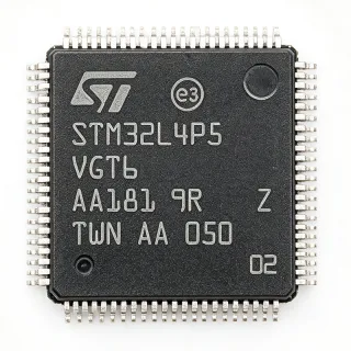
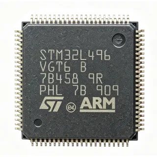
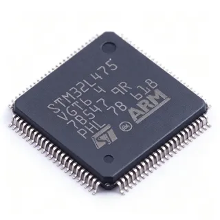
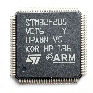
STM32F105VCT7 - 72MHz Cortex-M3 MCU 256KB Flash | STMicroelectronics
MPN: STM32F105VCT7 ✓ AktifSTM32F105VCT7 Ringkasan
An MCU (microcontroller unit) is a single-chip computer containing a processor core, program memory, data memory, and integrated peripherals. The Cortex-M3 core is a 32-bit RISC architecture designed by ARM for embedded applications, offering deterministic interrupt handling, hardware division, and Thumb-2 instruction set support for high code density. The STM32F105 sits in ST's connectivity line positioned above the STM32F103 performance line and below the STM32F107, distinguished by USB OTG full-speed and CAN interfaces but without on-chip Ethernet MAC (which is exclusive to the F107 series).
Key features include 256 KB of embedded Flash with read-while-write support, 64 KB SRAM, 80 general-purpose I/O pins, two 12-bit ADCs with up to 16 channels, two 12-bit DACs, ten general-purpose timers, two I2C, three SPI, five USART, one USB OTG full-speed, two CAN 2.0B interfaces, and an SDIO interface. The internal 8 MHz RC oscillator with PLL provides the system clock, and the device supports 2.0 V to 3.6 V operating voltage.
Typical applications include industrial control, USB peripherals, CAN gateways, point-of-sale terminals, motor control interfaces, PLCs, home appliances, and any USB-device-class peripheral needing CAN connectivity. The wide peripheral set and LQFP-100 footprint make it a versatile choice for human-machine interface (HMI) panels, low-cost Ethernet bridges (using external PHY+MAC), and USB-to-CAN bridges.
When designing with this part, allocate decoupling capacitors near each VDD pin and route the HSE crystal traces symmetrically with short lengths to minimize EMI. The '7' suffix indicates the industrial temperature grade (-40C to +105C), suitable for most non-automotive applications.
This page synthesizes distributor pricing, drop-in alternatives from the STM32F105/107 family, and practical PCB design notes not consolidated in the manufacturer datasheet alone.
Alternatif penggantian untuk STM32F105VCT7 — paket yang sama, pin-pada-pin kompatibel. Bagian paket yang berbeda memerlukan kerja ulang PCB diabaikan.
Variasi di dalam seri ini
Model-series yang sama yang kompatibel dengan penggantian STM32F105VCT7 (sama faktor bentuk dan footprint) — berbeda di dalam Timers, ADC, Package, DAC, Operating Temperature.
STM32F107VCT7
✅ Drop-In📋 Alternatif referensi (tidak dalam katalog)
STM32F105VCT6
✅ Drop-InKontak untuk harga
STM32F105VCT7TR
✅ Drop-In📋 Alternatif referensi (tidak dalam katalog)
STM32F103VCT6
✅ Drop-InKontak untuk harga
Lihat Datasheet →GD32F303VCT6
✅ Drop-In📋 Alternatif referensi (tidak dalam katalog)
STM32F105VCT7 Rating Maksimal & Karakteristik Listrik
| Core | ARM Cortex-M3 32-bit RISC |
| Frekuensi Bawah Maximum | 72 MHz |
| Program Memory (Flash) | 256 KB (256K x 8) |
| RAM | 64 KB |
| Number of I/O Pins | 80 |
| Paket | 100-LQFP (14x14 mm) |
| Tegangan Pemuat | 2.0 V to 3.6 V |
| Suhu Kerja | -40C to +105C (Grade 7) |
| ADC | 2 x 12-bit, up to 16 channels |
| DAC | 2 x 12-bit |
| Timers | 10 (general-purpose + advanced-control) |
| Communication Interfaces | 5 USART, 3 SPI, 2 I2C, 2 CAN, 1 USB OTG FS, 1 SDIO |
| Tipe Mounting | Surface Mount |
| Packaging | Tray |
| Status RoHS | Compliant |
Konfigurasi Pin STM32F105VCT7
| Pin produk 1 | PE2 — GPIO PE2, TRACECLK (trace clock) |
| Pin produk 2 | PE3 — GPIO PE3, TRACED0 |
| Pin produk 3 | PE4 — GPIO PE4, TRACED1 |
| Pin produk 4 | PE5 — GPIO PE5, TRACED2 |
| Pin produk 5 | PE6 — GPIO PE6, TRACED3 |
| Pin produk 6 | VBAT — Battery supply for RTC and backup registers |
| Pin produk 7 | PC13 — GPIO PC13, TAMPER-RTC (anti-tamper / RTC) |
| Pin produk 8 | PC14 — GPIO PC14, OSC32_IN (32.768 kHz crystal) |
| Pin produk 9 | PC15 — GPIO PC15, OSC32_OUT (32.768 kHz crystal) |
| Pin produk 10 | VSS_5 — Ground |
| Pin produk 11 | VDD_5 — Digital supply voltage 2.0-3.6 V |
| Pin produk 12 | OSC_IN — External clock input / HSE crystal input |
| Pin produk 13 | OSC_OUT — HSE crystal output |
| Pin produk 14 | NRST — Reset input (active low) |
| Pin produk 15 | PC0 — GPIO PC0, ADC1_IN10 |
| Pin produk 16 | PC1 — GPIO PC1, ADC1_IN11 |
| Pin produk 17 | PC2 — GPIO PC2, ADC1_IN12 |
| Pin produk 18 | PC3 — GPIO PC3, ADC1_IN13 |
| Pin produk 19 | VSSA — Analog ground |
| Pin produk 20 | VREF+ — ADC reference voltage positive |
| Pin produk 21 | VDDA — Analog supply voltage 2.0-3.6 V |
| Pin produk 22 | PA0 — GPIO PA0, WKUP, ADC1_IN0, TIM2_CH1 |
| Pin produk 23 | PA1 — GPIO PA1, ADC1_IN1, TIM2_CH2 |
| Pin produk 24 | PA2 — GPIO PA2, USART2_TX, ADC1_IN2, TIM2_CH3 |
| Pin produk 25 | PA3 — GPIO PA3, USART2_RX, ADC1_IN3, TIM2_CH4 |
| Pin produk 26 | VSS_4 — Ground |
| Pin produk 27 | VDD_4 — Digital supply voltage 2.0-3.6 V |
| Pin produk 28 | PA4 — GPIO PA4, SPI1_NSS, USART2_CK, ADC1_IN4 |
| Pin produk 29 | PA5 — GPIO PA5, SPI1_SCK, ADC1_IN5, DAC_OUT2 |
| Pin produk 30 | PA6 — GPIO PA6, SPI1_MISO, ADC1_IN6, TIM3_CH1, DAC_OUT1 |
| Pin produk 31 | PA7 — GPIO PA7, SPI1_MOSI, ADC1_IN7, TIM3_CH2 |
| Pin produk 32 | PB0 — GPIO PB0, ADC1_IN8, TIM3_CH3 |
| Pin produk 33 | PB1 — GPIO PB1, ADC1_IN9, TIM3_CH4 |
| Pin produk 34 | PB2 — GPIO PB2, BOOT1 |
| Pin produk 35 | VSS_3 — Ground |
| Pin produk 36 | VDD_3 — Digital supply voltage 2.0-3.6 V |
| Pin produk 37 | PE7 — GPIO PE7, TIM1_ETR |
| Pin produk 38 | PE8 — GPIO PE8, TIM1_CH1N |
| Pin produk 39 | PE9 — GPIO PE9, TIM1_CH1 |
| Pin produk 40 | PE10 — GPIO PE10, TIM1_CH2N |
| Pin produk 41 | PE11 — GPIO PE11, TIM1_CH2 |
| Pin produk 42 | PE12 — GPIO PE12, TIM1_CH3N |
| Pin produk 43 | PE13 — GPIO PE13, TIM1_CH3 |
| Pin produk 44 | PE14 — GPIO PE14, TIM1_CH4 |
| Pin produk 45 | PE15 — GPIO PE15, TIM1_BKIN |
| Pin produk 46 | PB10 — GPIO PB10, I2C2_SCL, USART3_TX |
| Pin produk 47 | PB11 — GPIO PB11, I2C2_SDA, USART3_RX |
| Pin produk 48 | VSS_2 — Ground |
| Pin produk 49 | VDD_2 — Digital supply voltage 2.0-3.6 V |
| Pin produk 50 | PB12 — GPIO PB12, SPI2_NSS, I2C2_SMBAI |
| Pin produk 51 | PB13 — GPIO PB13, SPI2_SCK, USART3_CK |
| Pin produk 52 | PB14 — GPIO PB14, SPI2_MISO, TIM1_CH2N |
| Pin produk 53 | PB15 — GPIO PB15, SPI2_MOSI, TIM1_CH3N |
| Pin produk 54 | PD8 — GPIO PD8, USART3_TX |
| Pin produk 55 | PD9 — GPIO PD9, USART3_RX |
| Pin produk 56 | PD10 — GPIO PD10 |
| Pin produk 57 | PD11 — GPIO PD11 |
| Pin produk 58 | PD12 — GPIO PD12, TIM4_CH1 |
| Pin produk 59 | PD13 — GPIO PD13, TIM4_CH2 |
| Pin produk 60 | PD14 — GPIO PD14, TIM4_CH3 |
| Pin produk 61 | PD15 — GPIO PD15, TIM4_CH4 |
| Pin produk 62 | VSS_1 — Ground |
| Pin produk 63 | VDD_1 — Digital supply voltage 2.0-3.6 V |
| Pin produk 64 | PC6 — GPIO PC6, TIM8_CH1, SDIO_D6 |
| Pin produk 65 | PC7 — GPIO PC7, TIM8_CH2, SDIO_D7 |
| Pin produk 66 | PC8 — GPIO PC8, TIM8_CH3, SDIO_D0 |
| Pin produk 67 | PC9 — GPIO PC9, TIM8_CH4, SDIO_D1 |
| Pin produk 68 | PA8 — GPIO PA8, USART1_CK, TIM1_CH1, MCO |
| Pin produk 69 | PA9 — GPIO PA9, USART1_TX, TIM1_CH2 |
| Pin produk 70 | PA10 — GPIO PA10, USART1_RX, TIM1_CH3 |
| Pin produk 71 | PA11 — GPIO PA11, USB_DM, CAN1_RX |
| Pin produk 72 | PA12 — GPIO PA12, USB_DP, CAN1_TX |
| Pin produk 73 | PA13 — GPIO PA13, JTMS, SWDIO |
| Pin produk 74 | VSS_6 — Ground |
| Pin produk 75 | VDD_6 — Digital supply voltage 2.0-3.6 V |
| Pin produk 76 | PA14 — GPIO PA14, JTCK, SWDCLK |
| Pin produk 77 | PA15 — GPIO PA15, JTDI, TIM2_CH1 |
| Pin produk 78 | PC10 — GPIO PC10, UART4_TX, SDIO_D2 |
| Pin produk 79 | PC11 — GPIO PC11, UART4_RX, SDIO_D3 |
| Pin produk 80 | PC12 — GPIO PC12, UART5_TX, SDIO_CK |
| Pin produk 81 | PD0 — GPIO PD0, CAN1_RX, OSC_IN (remap) |
| Pin produk 82 | PD1 — GPIO PD1, CAN1_TX, OSC_OUT (remap) |
| Pin produk 83 | PD2 — GPIO PD2, TIM3_ETR, SDIO_CMD |
| Pin produk 84 | PD3 — GPIO PD3, USART2_CTS |
| Pin produk 85 | PD4 — GPIO PD4, USART2_RTS |
| Pin produk 86 | PD5 — GPIO PD5, USART2_TX |
| Pin produk 87 | PD6 — GPIO PD6, USART2_RX |
| Pin produk 88 | PD7 — GPIO PD7, USART2_CK |
| Pin produk 89 | PB3 — GPIO PB3, JTDO, TIM2_CH2, SPI1_SCK (remap) |
| Pin produk 90 | PB4 — GPIO PB4, NJTRST, TIM3_CH1, SPI1_MISO (remap) |
| Pin produk 91 | PB5 — GPIO PB5, TIM3_CH2, SPI1_MOSI (remap), I2C1_SMBAI |
| Pin produk 92 | PB6 — GPIO PB6, I2C1_SCL, TIM4_CH1, USART1_TX |
| Pin produk 93 | PB7 — GPIO PB7, I2C1_SDA, TIM4_CH2, USART1_RX |
| Pin produk 94 | BOOT0 — Boot mode selection (0=main flash, 1=system memory bootloader) |
| Pin produk 95 | PB8 — GPIO PB8, TIM4_CH3, CAN1_RX (remap) |
| Pin produk 96 | PB9 — GPIO PB9, TIM4_CH4, CAN1_TX (remap) |
| Pin produk 97 | PE0 — GPIO PE0, TIM4_ETR |
| Pin produk 98 | PE1 — GPIO PE1 |
| Pin produk 99 | VSS_7 — Ground |
| Pin produk 100 | VDD_7 — Digital supply voltage 2.0-3.6 V |
Aplikasi Umum
STM32F105VCT7 cocok untuk 6 aplikasis: USB-to-CAN Industrial Bridge, Human-Machine Interface (HMI) Panel Controller, USB Barcode Scanner / HID Peripheral, Industrial Control PLC Module, Motor Control Interface Board, Medical Patient Monitoring Data Logger.
USB-to-CAN Industrial Bridge
The STM32F105VCT7's USB OTG full-speed peripheral combined with dual CAN 2.0B controllers (bxCAN) makes it ideal for USB-to-CAN gateway modules used in industrial automation, automotive diagnostics, and CANopen networks. The Cortex-M3 core handles USB CDC class enumeration and CAN frame transmission with deterministic latency, while the 64 KB SRAM buffers CAN traffic bursts. The 256 KB Flash is sufficient for USB stack (e.g., LibUSB) and CANopen/CANFestival protocols. Placed on a small PCB with USB Type-B connector and CAN transceiver (e.g., TJA1050), the part delivers a compact bridge solution operating at 72 MHz with 12 Mbps USB and 1 Mbit/s CAN simultaneously.
Direkomendasikan
Human-Machine Interface (HMI) Panel Controller
The 100-pin LQFP package provides 80 GPIO pins, ample for driving TFT displays, keypads, status LEDs, and external peripherals in HMI panels. The STM32F105VCT7's two 12-bit ADCs support touch-screen digitizer scanning, while the SPI and SDIO peripherals connect to display controllers and microSD storage. Running at 72 MHz, the Cortex-M3 executes FreeRTOS-based UI frameworks smoothly with the 64 KB SRAM accommodating frame buffers. Designers typically pair the MCU with an external TFT controller over SPI and use the FSMC-less GPIO bit-banging for parallel LCD interfaces up to QVGA resolution.
Direkomendasikan
USB Barcode Scanner / HID Peripheral
USB OTG full-speed with on-chip PHY enables direct USB device, host, or dual-role operation without external transceivers, ideal for barcode scanners, RFID readers, and HID peripherals. The STM32F105VCT7 runs USB HID class firmware at 72 MHz with minimal CPU overhead, leaving the 64 KB SRAM and 256 KB Flash available for application code, decode libraries, and buffer storage. The 12 Mbps USB FS bandwidth accommodates keyboard, mouse, barcode wedge, and custom HID reports with sub-1 ms latency. Designers can integrate a USB Type-C interface directly using PA11/PA12 pins with proper ESD protection.
Direkomendasikan
Industrial Control PLC Module
With dual CAN, five USARTs, three SPI, and two I2C interfaces, the STM32F105VCT7 serves as the main processor for compact PLC modules and industrial control boards. The Cortex-M3 at 72 MHz executes IEC 61131-3 runtimes or ladder-logic interpreters, while the 80 GPIO pins drive relays, optocouplers, and isolated digital I/O. The wide 2.0-3.6 V supply tolerance accommodates industrial 24 V systems stepped down to 3.3 V via isolated DC-DC converters. The 105C operating temperature (Grade 7) supports factory-floor cabinets without additional cooling.
Direkomendasikan
Motor Control Interface Board
The STM32F105VCT7's ten timers (including one advanced-control timer with complementary PWM outputs) provide ample PWM channels for brushless DC (BLDC) and stepper motor control interface boards. The 12-bit ADCs sample current and back-EMF signals at up to 1 MSPS, while the Cortex-M3 executes field-oriented control (FOC) algorithms at 72 MHz. Designers typically pair the MCU with external gate drivers (e.g., ST L6234) and use the CAN peripherals for multi-axis communication. The 64 KB SRAM limits FOC to single-axis or basic dual-axis implementations.
Direkomendasikan
Medical Patient Monitoring Data Logger
Medical-grade patient monitoring peripherals (pulse oximeters, thermometers, glucose meters) leverage the STM32F105VCT7's USB OTG for data transfer to PCs, dual CAN for hospital network connectivity, and SDIO for local data storage on microSD cards. The 256 KB Flash stores firmware with embedded USB stack, while the 64 KB SRAM buffers continuous monitoring data. The Cortex-M3 deterministic interrupt response (12-cycle tail-chaining) ensures accurate sensor sampling timing. The -40C to +105C temperature range supports battery-powered portable medical devices.
Direkomendasikan
Ringkasan Produk Direkomendasikan
Data referensi engineering untuk STM32F105VCT7 — pembandingan, panduan desain, dan informasi konformitas.
Panduan Pemilihan
Pembandingan dengan Alternatif
| Parameter Umum | Produk Ini | STM32F107VCT7 | STM32F105VCT6 | STM32F105VCT7TR | STM32F103VCT6 | GD32F303VCT6 |
|---|---|---|---|---|---|---|
| Brand | STMicroelectronics | STMicroelectronics | STMicroelectronics | STMicroelectronics | STMicroelectronics | GigaDevice |
| Package | LQFP-100 (14x14 mm) | LQFP-100 (14x14) - same | LQFP-100 (14x14) - same | LQFP-100 (14x14) - same | LQFP-100 (14x14) - same | LQFP-100 (14x14) - same |
| Core | Cortex-M3 @ 72 MHz | Cortex-M3 @ 72 MHz | Cortex-M3 @ 72 MHz | Cortex-M3 @ 72 MHz | Cortex-M3 @ 72 MHz | Cortex-M3 @ 120 MHz |
| Flash | 256 KB | 256 KB | 256 KB | 256 KB | 256 KB | 256 KB |
| SRAM | 64 KB | 64 KB | 64 KB | 64 KB | 48 KB | 48 KB |
| USB | USB OTG FS | USB OTG FS | USB OTG FS | USB OTG FS | USB FS (no OTG) | USB FS (no OTG) |
| CAN | 2 x CAN 2.0B | 2 x CAN 2.0B | 2 x CAN 2.0B | 2 x CAN 2.0B | 1 x CAN 2.0B | 1 x CAN 2.0B |
| Ethernet MAC | No | Yes (10/100 MII/RMII) | No | No | No | No |
| Operating Temperature | -40C to +105C | -40C to +105C | -40C to +85C | -40C to +105C | -40C to +85C | -40C to +85C |
Diferensiator Kunci
- USB OTG with dual CAN in connectivity line (vsSTM32F103VCT6)
- No on-chip Ethernet MAC for cost optimization (vsSTM32F107VCT7)
- Industrial temperature grade with Grade 7 rating (vsSTM32F105VCT6)
Catatan Desain
The STM32F105VCT7 has 7 VDD pins (pins 11, 27, 36, 49, 63, 75, 100) and corresponding VSS pins that must each be decoupled with a 100 nF ceramic capacitor placed within 5 mm of each pin. Add a bulk 10 uF tantalum or ceramic capacitor near the regulator output. VDDA requires a separate 10 nF + 1 uF filter; tying VDDA directly to VDD without filtering degrades ADC SNR by 5-10 dB. VBAT must be tied to VDD if RTC/battery backup is unused, never left floating.
Route the HSE crystal traces (OSC_IN/OSC_OUT) symmetrically with traces under 5 mm length and a ground guard ring to prevent crosstalk with switching nodes. For USB, route PA11/PA12 as a 90-ohm differential pair with matched length within 2 mm and a ground plane underneath. The SDIO bus to microSD cards must have series 33-ohm resistors for signal integrity at 48 MHz clock. Keep the BOOT0 pin accessible via a test pad or jumper for firmware recovery.
Do not assume the F105 has Ethernet like the F107 - the F105 has the MAC registers reserved but no Ethernet peripheral. The '7' suffix indicates Grade 7 (-40C to +105C), not 125C - for 125C automotive use, look at STM32F105VCT7B or AEC-Q100 qualified parts. When migrating from STM32F103 firmware, verify bxCAN register initialization - the F105/F107 bxCAN has enhanced filter banks that differ from F103. USB OTG requires the PA11/PA12 pins to be at 3.3 V; lower VDD voltages disable USB PHY.
Informasi Konformitas
RoHS compliant per ST product page. Industrial temperature grade (Grade 7, -40C to +105C), NOT AEC-Q100 qualified - for automotive designs use STM32F105VCT7B or qualified variants.