ディスクリート半導体
サブカテゴリ
製品 (1814)

STU16N65M5 - 650V N-Channel Power MOSFET | STMicroelectronics
The STU16N65M5 is an N-channel Power MOSFET from STMicroelectronics, part of the MDmesh M5 series, designed for high-efficiency power conversion applications. It features a breakdown voltage of 650V and a continuous drain current of 16A at 25°C, with a low on-resistance of 0.29 ohm (typical) to minimize conduction losses. The device is housed in an IPAK (TO-251) package, which offers a compact footprint with a metal tab for thermal dissipation, suitable for through-hole mounting in power supplies and industrial equipment. A Power MOSFET is a type of field-effect transistor optimized for switching and amplification of power. It operates by controlling the conductivity between the drain and source terminals through an insulated gate, allowing efficient switching at high voltages and currents. Power MOSFETs are fundamental building blocks in power electronics, serving as switches in DC-DC converters, AC-DC power supplies, motor drives, and lighting systems. They are part of the broader category of discrete semiconductors, which also includes diodes, thyristors, and IGBTs, each tailored for specific power handling and switching requirements. Key features of the STU16N65M5 include a very low gate charge (Qg) of 38 nC (typical), which enables fast switching and reduces driver losses, and a high dv/dt capability for robust performance in hard-switching topologies. The device also offers a wide operating junction temperature range from -55°C to +150°C, ensuring reliability in harsh environments. Its avalanche ruggedness is rated at 400 mJ (single pulse), making it suitable for applications where inductive loads may cause voltage spikes. Technically, the MDmesh M5 series utilizes a proprietary strip layout technology that reduces on-resistance and gate charge simultaneously, achieving a figure of merit (RDS(on) x Qg) that is among the best in its class. This technology enhances the device's efficiency in high-frequency switching applications, where both conduction and switching losses are critical. The STU16N65M5 also features a built-in diode with fast recovery characteristics, reducing reverse recovery losses in bridge topologies. Typical applications include switch-mode power supplies (SMPS) for consumer and industrial electronics, power factor correction (PFC) circuits, LED lighting drivers, and solar inverters. Its 650V rating provides ample margin for universal input (85-265V AC) power supplies, while the low on-resistance ensures high efficiency in continuous conduction mode. When designing with the STU16N65M5, ensure proper gate drive voltage (typically 10V) to fully enhance the channel and minimize on-resistance. A gate resistor may be needed to control switching speed and reduce EMI. Thermal management is crucial: the IPAK package's tab should be soldered to a sufficient copper area or heatsink to dissipate heat, especially at high currents. Always consider the device's SOA (Safe Operating Area) and avalanche ratings when designing for inductive loads.

STW11NK90Z - 900V N-Channel Power MOSFET | STMicroelectronics
The STW11NK90Z is an N-channel Power MOSFET from STMicroelectronics, designed for high-voltage switching applications. It features a drain-source voltage (VDS) of 900V, a continuous drain current (ID) of 9.5A at 25°C, and a low on-resistance (RDS(on)) of 0.85 ohm. The device is housed in a TO-247 package, which provides excellent thermal performance for high-power applications. A Power MOSFET is a type of field-effect transistor designed to handle significant power levels. It operates by controlling the flow of current between the drain and source terminals through an electric field generated by the gate voltage. Power MOSFETs are essential components in power electronics, serving as switches in power supplies, motor drives, and inverters. They are part of the broader category of discrete semiconductors, which also includes diodes, thyristors, and IGBTs. Key features of the STW11NK90Z include a high voltage rating of 900V, making it suitable for applications such as switch-mode power supplies (SMPS), power factor correction (PFC) circuits, and high-voltage DC-DC converters. The low on-resistance minimizes conduction losses, improving overall efficiency. The device also features a fast switching speed, which is critical for reducing switching losses in high-frequency applications. The STW11NK90Z utilizes STMicroelectronics' advanced PowerMESH technology, which provides a robust and reliable structure. The device has a maximum junction temperature of 150°C and is available in a TO-247 package, which offers a low thermal resistance of 0.5°C/W, enabling efficient heat dissipation. The device is RoHS compliant and lead-free, meeting environmental standards. Typical applications include high-voltage power supplies, industrial motor drives, and renewable energy inverters. The device's high voltage rating and low on-resistance make it ideal for these applications, where efficiency and reliability are paramount. When designing with the STW11NK90Z, it is important to consider the gate drive requirements. The device has a gate threshold voltage of 3V to 5V, and a gate charge of 45nC, which should be considered when designing the gate drive circuit. Additionally, proper heat sinking is essential to maintain the junction temperature within safe limits.
STW12N60M2 - 600V 12A N-Channel MDmesh M2 MOSFET | STMicroelectronics
The STW12N60M2 is an N-channel Power MOSFET from STMicroelectronics' MDmesh M2 series, designed for high-efficiency power conversion applications. It features a 600V drain-source breakdown voltage and a continuous drain current of 12A at 25°C, with a low on-resistance of 0.38 ohm (typical) and a fast body diode. The device is housed in a TO-247 package, which provides excellent thermal performance for high-power designs. A Power MOSFET is a type of field-effect transistor optimized for switching and amplification in power electronics. It operates by controlling the conductivity between the drain and source terminals through an insulated gate voltage. Power MOSFETs are essential components in switch-mode power supplies, motor drives, and inverters, where they handle high voltages and currents with minimal conduction and switching losses. They are part of the broader family of power semiconductor devices, which also includes IGBTs and thyristors, but MOSFETs are preferred for high-frequency switching due to their fast switching speed and low drive power. Key features of the STW12N60M2 include a low gate charge (Qg) of 30 nC (typical), which reduces switching losses and enables high-frequency operation. The device also offers a high dv/dt capability and is avalanche-rated, ensuring robustness in harsh environments. The MDmesh M2 technology provides an excellent figure of merit (RDS(on) x Qg), making it suitable for applications where efficiency is critical. The STW12N60M2 utilizes STMicroelectronics' MDmesh M2 vertical structure, which combines a low on-resistance with a fast intrinsic diode. This technology reduces conduction and switching losses, improving overall system efficiency. The device is fully isolated and RoHS compliant, meeting modern environmental standards. Typical applications include switch-mode power supplies (SMPS), power factor correction (PFC) circuits, LED lighting drivers, and solar inverters. The high voltage rating and low on-resistance make it ideal for 600V-class power conversion systems. When designing with this device, ensure proper gate drive voltage (typically 10V) to achieve the lowest on-resistance. A gate resistor may be needed to control switching speed and reduce EMI. Adequate heatsinking is required for high-current operation, as power dissipation can be significant.

STW12NK95Z - 950V 10A Zener SuperMESH MOSFET | STMicroelectronics
The STW12NK95Z is an N-channel Power MOSFET from STMicroelectronics, featuring a 950V drain-source breakdown voltage and a continuous drain current of 10A at case temperature (Tc). It is housed in a TO-247-3 through-hole package, designed for high-voltage power switching applications. The device offers a typical on-resistance of 0.69 ohm (maximum 0.90 ohm) and a power dissipation of 230W at Tc, making it suitable for demanding power conversion circuits. A Power MOSFET is a type of field-effect transistor optimized for high power and high voltage switching. It operates by controlling the conductivity between the drain and source terminals through an insulated gate voltage. Power MOSFETs are essential components in power electronics, serving as switches in power supplies, inverters, and motor drives. They belong to the broader discrete semiconductor family, alongside diodes, IGBTs, and thyristors. Key features include Zener protection, which safeguards the gate oxide from overvoltage transients, and minimized gate charge for faster switching and reduced drive losses. The device is 100% avalanche tested, ensuring ruggedness under inductive load conditions, and offers extremely high dv/dt capability for reliable fast-switching operation. The SuperMESH technology, an evolution of ST's strip-based PowerMESH layout, significantly reduces on-resistance while maintaining high breakdown voltage. This results in lower conduction losses and improved efficiency, while minimized gate charge enables higher frequency operation and smaller magnetic components. Typical applications include switch-mode power supplies (SMPS), power factor correction (PFC) circuits, high-voltage DC-DC converters, and lighting systems where efficiency and reliability are critical. When designing with this device, ensure a proper gate drive voltage (typically 10V) to fully enhance the channel and minimize conduction losses, and provide adequate heatsinking since the device can dissipate up to 230W at maintained case temperature.
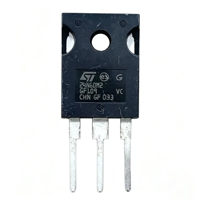
STW18N60M2 - 650V 18A N-Channel Power MOSFET | STMicroelectronics
The STW18N60M2 is an N-channel Power MOSFET manufactured by STMicroelectronics, featuring a breakdown voltage of 650V and a continuous drain current of 18A at 25°C. It is housed in a TO-247 package, which is a through-hole package suitable for high-power applications. This device is part of the MDmesh M2 series, which utilizes ST's advanced strip layout technology to achieve low on-resistance and reduced switching losses. A power MOSFET is a type of field-effect transistor designed to handle significant power levels in switching and amplification applications. It operates by controlling the flow of current through a semiconductor channel using an electric field, and it is widely used in power electronics for its high switching speed and efficiency. Power MOSFETs are a subset of discrete semiconductors, which are fundamental building blocks in power management and conversion systems. Key features of the STW18N60M2 include a low typical on-resistance of 0.19 ohm (at VGS=10V, ID=9A), a high avalanche ruggedness with an energy rating of 700 mJ, and a fast body diode with low reverse recovery charge. The device also offers a wide operating junction temperature range from -55°C to +150°C, making it suitable for demanding environments. The TO-247 package provides excellent thermal performance with a junction-to-case thermal resistance of 0.6°C/W, enabling efficient heat dissipation. The STW18N60M2 is built using ST's MDmesh M2 technology, which combines a vertical structure with a strip layout to minimize on-resistance and gate charge. This results in improved figure of merit (FOM) compared to previous generations, leading to higher efficiency in power conversion circuits. The device is designed for hard-switching topologies and offers a low gate charge of 45 nC, reducing driver requirements and switching losses. Typical applications include switch-mode power supplies (SMPS), power factor correction (PFC) circuits, and high-frequency DC-DC converters. In an SMPS, the STW18N60M2 can be used as the main switching element in the primary side, handling high voltage and current with minimal losses. Its low on-resistance ensures high efficiency, while its fast switching characteristics reduce electromagnetic interference (EMI). When designing with this device, ensure proper gate drive voltage (typically 10V) to achieve the lowest on-resistance. The device is not internally protected against overcurrent, so external current sensing and protection circuitry are recommended. Additionally, a proper snubber circuit may be required to manage voltage spikes during switching transitions.
STW20N60M2 - 600V 20A N-Channel Power MOSFET | STMicroelectronics
The STW20N60M2 is an N-channel Power MOSFET from STMicroelectronics' MDmesh M2 series, designed for high-efficiency power conversion applications. It features a breakdown voltage of 600V and a continuous drain current of 20A at 25°C, with a low on-resistance of 0.19 ohm typical. The device is housed in a TO-247 package, which provides excellent thermal performance for high-power applications. A Power MOSFET is a type of field-effect transistor optimized for switching and amplification of power. It operates by controlling the conductivity between the drain and source terminals through an insulated gate voltage. Power MOSFETs are essential components in power electronics, serving as switches in DC-DC converters, AC-DC power supplies, motor drives, and inverters. They are preferred for their fast switching speeds, high input impedance, and low drive power requirements compared to bipolar junction transistors. Key features of the STW20N60M2 include a low gate charge (Qg) of 45 nC, which reduces switching losses and enables high-frequency operation. The device also offers a fast body diode with low reverse recovery charge, making it suitable for bridge topologies. The MDmesh M2 technology provides an excellent figure of merit (RDS(on) x Qg), balancing conduction and switching losses for optimal efficiency. The STW20N60M2 utilizes a vertical DMOS structure with a striped layout, optimizing current distribution and thermal performance. The TO-247 package offers a low thermal resistance of 0.5°C/W (junction-to-case), allowing efficient heat dissipation. The device is avalanche-rated, with an avalanche energy of 1.2 J, ensuring robustness in inductive load switching. Typical applications include switch-mode power supplies (SMPS), power factor correction (PFC) circuits, solar inverters, and motor drives. The high voltage rating and low on-resistance make it ideal for 400V bus systems and 3-phase rectification. In PFC boost converters, the low gate charge enables high switching frequencies, reducing magnetic component size. When designing with this device, ensure proper gate drive voltage (typically 10V to 15V) to achieve low RDS(on). A gate resistor may be needed to control switching speed and reduce EMI. Adequate heatsinking is essential for continuous operation at high currents, as power dissipation can exceed 100W in worst-case conditions.
STW26N60M2 - 600V 26A N-Channel Power MOSFET | STMicroelectronics
The STW26N60M2 is an N-channel Power MOSFET manufactured by STMicroelectronics, designed for high-efficiency power conversion applications. It features a breakdown voltage of 600V and a continuous drain current of 26A at 25°C, making it suitable for a wide range of industrial and consumer power systems. The device is housed in a TO-247 package, which provides excellent thermal performance and is widely used in power electronics. A Power MOSFET is a type of field-effect transistor specifically designed to handle high voltages and currents in switching and amplification applications. It operates by controlling the flow of current through a semiconductor channel using an electric field, offering fast switching speeds and low on-resistance compared to bipolar transistors. Power MOSFETs are essential components in power management systems, where they function as switches in DC-DC converters, motor drives, and power supplies, enabling efficient energy conversion and regulation. Key features of the STW26N60M2 include a low on-resistance (RDS(on)) of typically 0.125 ohm at VGS=10V, which minimizes conduction losses and improves overall efficiency. The device also offers a fast switching performance with a total gate charge (Qg) of 78 nC, reducing switching losses in high-frequency applications. Additionally, it has a wide operating temperature range from -55°C to +150°C, ensuring reliability in harsh environments. The TO-247 package provides a low thermal resistance of 0.5°C/W (junction-to-case), enabling efficient heat dissipation. The STW26N60M2 utilizes STMicroelectronics' MDmesh M2 technology, which combines a vertical structure with a deep trench gate to achieve a good trade-off between on-resistance and switching performance. This technology enhances the device's robustness against avalanche breakdown and improves its body diode characteristics, making it suitable for bridge topologies and inductive load switching. The device also features a built-in gate-source ESD protection, enhancing its durability during handling and operation. Typical applications include switch-mode power supplies (SMPS), power factor correction (PFC) circuits, motor control, and uninterruptible power supplies (UPS). In these applications, the STW26N60M2 provides efficient switching and low conduction losses, contributing to higher system efficiency and reduced heat generation. Its high voltage rating and current capability make it ideal for 400V and 600V bus systems commonly found in industrial and telecom power supplies. When designing with this device, ensure proper gate driving to minimize switching losses and avoid parasitic turn-on. A gate resistor in the range of 10-100 ohm is recommended to control the switching speed and reduce EMI. Additionally, adequate heat sinking is required to maintain the junction temperature within safe limits, especially when operating at high currents and ambient temperatures.
STW30N60M2 - 600V 30A N-Channel Power MOSFET | STMicroelectronics
The STW30N60M2 is an N-channel Power MOSFET from STMicroelectronics' MDmesh M2 series, designed for high-efficiency power conversion applications. It features a breakdown voltage of 600V and a continuous drain current of 30A at 25°C, with a low on-resistance of 0.098 ohm (typical) and a fast body diode. The device is housed in a TO-247 package, which provides excellent thermal performance for high-power applications. A power MOSFET is a type of field-effect transistor designed to handle significant power levels in switching and amplification circuits. It operates by controlling the flow of current through a semiconductor channel using an electric field, offering high switching speeds and low conduction losses. Power MOSFETs are fundamental building blocks in power electronics, forming the basis of switch-mode power supplies, motor drives, and inverters. They are part of the broader category of discrete semiconductors, which also includes diodes, thyristors, and IGBTs. Key features of the STW30N60M2 include a low gate charge (Qg) of 60 nC (typical), which reduces switching losses and enables high-frequency operation. The device also offers a wide safe operating area (SOA) and is avalanche-rated, ensuring robustness in harsh environments. The TO-247 package has a thermal resistance of 0.5°C/W (junction-to-case), allowing efficient heat dissipation when mounted on a suitable heatsink. The STW30N60M2 utilizes STMicroelectronics' MDmesh M2 technology, which combines a vertical structure with a deep trench gate to achieve low on-resistance and reduced capacitance. This results in improved figure of merit (FOM) compared to previous generations, making it suitable for high-efficiency designs. The device also features a fast intrinsic body diode with low reverse recovery charge, which is critical for bridge topologies where diode recovery losses can dominate. Typical applications include switch-mode power supplies (SMPS), power factor correction (PFC) circuits, solar inverters, and motor drives. In an SMPS, the STW30N60M2 can be used as the main switching element in a flyback or forward converter, where its low RDS(on) minimizes conduction losses and its fast switching reduces transition losses. For PFC, the device's high voltage rating and low gate charge enable efficient boost converters operating at high frequencies. When designing with the STW30N60M2, ensure proper gate drive voltage (typically 10V to 15V) to fully enhance the channel and minimize on-resistance. The device is not internally protected against overcurrent, so an external current-sense resistor or fuse is recommended. Additionally, a gate resistor (e.g., 10 ohm) may be used to dampen ringing caused by parasitic inductance and capacitance.
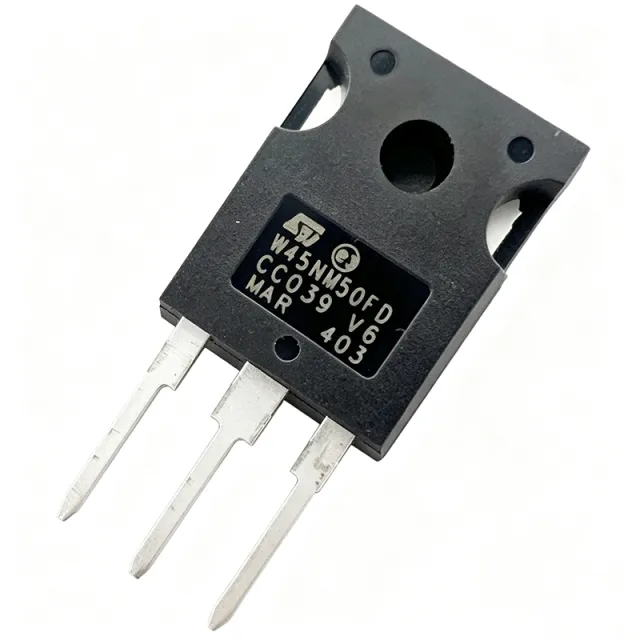
STW45NM50 - 45A, 500V N-Channel Power MOSFET | STMicroelectronics
The STW45NM50 is an N-channel Power MOSFET from STMicroelectronics, designed for high-efficiency power conversion applications. It features a drain-source voltage (VDS) of 500V, a continuous drain current (ID) of 45A at 25°C, and a low on-resistance (RDS(on)) of 0.09 ohm. The device is housed in a TO-247 package, which provides excellent thermal performance for high-power applications. A Power MOSFET is a type of field-effect transistor optimized for switching and amplification of power. It operates by controlling the flow of current through a semiconductor channel using an electric field, offering fast switching speeds and low conduction losses. Power MOSFETs are fundamental building blocks in power electronics, forming the basis of power management systems, motor drives, and switch-mode power supplies. They are part of the broader category of discrete semiconductors, which also includes diodes, thyristors, and IGBTs. Key features of the STW45NM50 include a low gate charge (Qg) of 120 nC, which enables fast switching and reduced driver requirements. The device also features a high avalanche ruggedness, with an avalanche energy rating of 1.2 J, making it suitable for applications where inductive loads are present. The TO-247 package offers a low thermal resistance of 0.5°C/W, allowing efficient heat dissipation in high-power designs. The STW45NM50 utilizes ST's proprietary MDmesh technology, which reduces on-resistance and gate charge compared to conventional MOSFETs. This technology enhances the device's efficiency and switching performance, making it ideal for high-frequency power conversion circuits. The device also includes an integrated body diode with fast recovery characteristics, reducing switching losses in bridge topologies. Typical applications include switch-mode power supplies (SMPS), power factor correction (PFC) circuits, motor drives, and uninterruptible power supplies (UPS). The high voltage rating and low on-resistance make it suitable for 400V and 500V bus systems commonly found in industrial and telecom equipment. When designing with this device, ensure proper gate drive voltage (typically 10V to 15V) to fully enhance the channel and minimize conduction losses. The device is RoHS compliant and halogen-free, meeting modern environmental standards. For automotive applications, consider the AEC-Q101 qualified variants if available.

STW45NM60 - 600V 45A MDmesh Power MOSFET | STMicroelectronics
The STMicroelectronics STW45NM60 is an N-channel 600 V, 45 A MDmesh Power MOSFET housed in a TO-247-3 through-hole package, designed using STMicroelectronics' proprietary MDmesh technology that combines a multiple-drain process with the company's PowerMESH horizontal layout. The device features a typical on-resistance of 90 mΩ at 10 V gate drive and 110 mΩ at 4.5 V, with a maximum continuous drain current of 45 A at Tc and a power dissipation rating of 417 W at Tc. A Power MOSFET is a voltage-controlled semiconductor switch used to efficiently switch and conduct current in power-conversion circuits. N-channel MOSFETs are the most common type due to their lower on-resistance per unit area compared to P-channel counterparts. The MDmesh family sits within STMicroelectronics' high-voltage MOSFET hierarchy (MDmesh -> PowerMESH -> Power MOSFET -> discrete semiconductor), targeting switched-mode power supply (SMPS) primary-side switches, motor-control inverters, and uninterruptible power supply (UPS) stages. Key features include a 600 V drain-source breakdown voltage rating, 90 mΩ typical Rds(on) at Vgs=10 V, and an outstanding dv/dt capability plus excellent avalanche ruggedness. The strip-based process yields overall dynamic performance that is significantly better than competing similar products. The TO-247 package provides high thermal-mass dissipation needed at 45 A continuous operation. Typical applications include high-power switched-mode power supply (SMPS) primary switches, three-phase inverter bridges for motor drives, induction heating, welding converters, photovoltaic string inverters, and uninterruptible power supply (UPS) front-end PFC and bridge stages. The 600 V rating provides ample headroom above 400 V PFC bus rails. When designing with this device, gate-drive voltage must reach 10 V for full enhancement to achieve the lowest Rds(on). At full 45 A load, ensure heatsink thermal resistance keeps Tj below 150 °C, and gate-source protection with a Zener clamp is recommended in motor-control environments where dv/dt stresses are severe. This page synthesizes distributor pricing, drop-in alternatives, and practical design notes not found in the manufacturer datasheet.
STW45NM60-H - 600V 45A MDmesh N-Channel Power MOSFET | STMicroelectronics
The STMicroelectronics STW45NM60-H is an N-channel 600 V, 45 A MDmesh power MOSFET housed in a TO-247-3 through-hole package with a typical on-resistance of 90 mΩ. Built on ST's revolutionary MDmesh technology that pairs a multiple-drain process with the proprietary PowerMESH horizontal layout, it achieves an outstandingly low RDS(on), high dv/dt capability, and excellent avalanche ruggedness for demanding high-voltage switching. Key specifications include a 600 V drain-source breakdown voltage (650 V at TJMAX), 45 A continuous drain current at 25 °C case, and 417 W total power dissipation. The device offers a typical on-resistance of 0.09 Ω at VGS = 10 V, gate threshold of 4 V, and 100% avalanche-tested ruggedness. The TO-247-3 through-hole package delivers superior thermal dissipation for high-current switching topologies. What is a MOSFET? A MOSFET (Metal-Oxide-Semiconductor Field-Effect Transistor) is a voltage-controlled semiconductor switch used for power conversion. Within the MOSFET family, power MOSFETs are classified into categories such as planar MOSFETs, trench MOSFETs, and super-junction (charge-balance) MOSFETs. The MDmesh family - where this STW45NM60-H belongs - is a super-junction N-channel MOSFET optimized for high-voltage (>500 V) switching applications. The STW45NM60-H is a discrete power transistor used in power management and conversion circuits. Architecture-wise, the MDmesh cell combines a multi-drain vertical structure with horizontal PowerMESH metallization, producing a higher power density than competing planar MOSFETs while lowering conduction losses. The strip-layout technique minimizes dynamic drain-source capacitance, reducing switching losses in hard-switched converters such as PFC stages and half-bridge converters. Typical applications include switched-mode power supplies (SMPS) with PFC, high-voltage DC-DC converters, industrial motor drives, uninterruptible power supplies (UPS), welding equipment, and induction-heating inverter stages operating from rectified 230 V or 400 V mains. When designing with this device, ensure adequate heat-sinking - the 417 W dissipation rating is only attainable with a substantial thermal interface. For high-frequency hard-switching topologies, gate-drive resistors in the 10-47 Ω range limit ringing, while a small RC snubber across the drain-source terminals mitigates voltage spikes caused by transformer leakage inductance. This page synthesizes distributor pricing, drop-in alternatives, and practical design notes that are not available in the manufacturer datasheet alone, giving design engineers a complete parametric view for sourcing decisions.

STX83003-AP - 400V NPN High-Voltage Fast Switch BJT | STMicro
The STMicroelectronics STX83003-AP is a 400 V, 1 A NPN bipolar junction transistor built on high-voltage Multi Epitaxial Planar technology and housed in a TO-92-3 through-hole package with Ammo Pack (AP) tape packaging. Designed for high switching speeds and medium voltage capability, the device uses a Cellular Emitter structure with planar edge termination to enhance switching speeds while maintaining a wide Reverse Bias Safe Operating Area (RBSOA). What is a high-voltage fast-switching NPN BJT? It is a bipolar junction transistor whose collector-emitter breakdown voltage (VCEO) is rated at several hundred volts while still providing sub-microsecond fall times, enabling efficient drive of inductive loads such as fluorescent lamp ballasts, deflection circuits, and switching-mode power supply snubbers. Within the transistor hierarchy, this places STX83003-AP as NPN BJT -> bipolar transistor -> discrete semiconductor -> semiconductor device. Key specifications include a collector-emitter breakdown voltage of 400 V, continuous collector current of 1 A, total power dissipation of 1.5 W in free air, DC current gain (hFE) minimum of 16 at 350 mA / 5 V, and a low VCE saturation characteristic that minimizes conduction loss in switching applications. The TO-92-3 package is the industry-standard through-hole outline, allowing PCB replacement without footprint rework for designers migrating from legacy ZTX or MPSA-style high-voltage transistors. Architecture-wise, the Multi Epitaxial Planar process delivers narrow dynamic-parameter spread and minimum lot-to-lot spread for reliable operation across production batches. The Cellular Emitter geometry and planar edge termination suppress localized hot-spotting at high dV/dt, supporting a wide RBSOA that is critical when the transistor turns off inductive loads where the collector voltage spikes above the DC rail. Typical applications include electronic ballasts for fluorescent lighting, switching regulators, high-voltage DC-DC converters, deflection circuits for CRT displays, and general-purpose medium-voltage N power switching where a small-signal BJT such as the 2N5551 lacks voltage headroom. Compared with the surface-mount STN83003 in SOT-223, the STX83003-AP offers a TO-92 through-hole form factor favored by hobbyist, replacement, and through-hole industrial designs. Designers should observe a maximum junction temperature of 150°C and derate dissipation according to the TO-92 thermal resistance (approximately 200°C/W free air). A small clip-on heatsink or PCB copper thermal relief noticeably improves RBSOA margin in continuous high-voltage switching service. A base-drive resistor of 1 kΩ to 10 kΩ is recommended to control turn-off dV/dt and limit stored base charge. This page combines distributor pricing, parametric comparison with drop-in equivalents, and design guidance not consolidated in the manufacturer datasheet.

SUM60061EL-GE3 - 80V 150A P-Channel TrenchFET MOSFET | Vishay
The Vishay Siliconix SUM60061EL-GE3 is a P-Channel TrenchFET power MOSFET rated at 80 V VDS and 150 A continuous drain current (Tc) with 375 W power dissipation (Tc), housed in a surface-mount TO-263 (D2PAK) package. The '-GE3' suffix indicates the device is supplied lead-free and halogen-free, fully RoHS-compliant, with a matte-tin finish qualified for high-reflow soldering profiles. It is a member of the SUM6xxxx TrenchFET family, a line of P-channel MOSFETs designed for high-current switching applications where low on-resistance and high avalanche ruggedness are required. A P-channel MOSFET (PMOS) is a majority-carrier field-effect transistor whose channel is composed of p-type carriers (holes). PMOS devices simplify high-side switching circuits because they turn ON when the gate is pulled below the source, eliminating the need for a bootstrap or charge-pump circuit that N-channel high-side switches typically require. The SUM6xxxx family falls under the broader hierarchy of: P-channel MOSFET -> power MOSFET -> discrete semiconductor -> power management component. Key features of the SUM60061EL-GE3 include an extremely low typical on-resistance (RDS(on)) in the single-digit milliohm range at VGS = -10 V, fast switching, and 100% Rg and UIS (unclamped inductive switching) tested for avalanche ruggedness. The TO-263 (D2PAK) surface-mount package exposes a large metal tab for direct PCB heatsinking, enabling continuous high-current operation on FR-4 boards with proper copper-pour design. The SUM60061EL-GE3 uses Vishay's proprietary TrenchFET silicon technology, which etches vertical trenches into the silicon die to dramatically increase channel density per unit area. This produces lower RDS(on) per die size than planar MOSFETs, reducing conduction losses and improving thermal performance in compact surface-mount designs. Typical applications include power-OR-ing in redundant supply systems, battery protection and load switching in 48 V telecom rails, motor-drive reverse-battery protection, eMobility and forklift controllers, hot-swap circuits on server backplanes, and synchronous-rectifier secondary-side switching in industrial SMPS. Designers favor it when a logic-level P-channel high-side switch must drop minimal voltage at high current. When designing with this device, ensure VGS(th) is exceeded by a healthy margin at logic high levels, and provide adequate copper-pour area on the TO-263 tab to keep junction temperature below 175 C. Because P-channel MOSFETs carry current through the body diode during dead-time in half-bridge topologies, account for reverse-recovery loss if used as a synchronous rectifier. The lead-free (Sn) finish supports peak reflow temperatures up to 260 C per IPC/JEDEC J-STD-020. This page synthesizes distributor pricing, drop-in TrenchFET alternatives, and practical PCB thermal guidance not found in the manufacturer datasheet alone.

SZESD1014MUTAG - 11V 30A Low-Capacitance TVS Array | onsemi
The onsemi SZESD1014MUTAG is a low-capacitance ESD protection diode array with an 11 V clamp voltage and 30 A peak pulse current, packaged in a surface-mount 10-UDFN measuring 2.6 mm by 2.6 mm. It is designed to protect high-speed data lines from ESD, EFT, and lightning-related transients while minimizing signal-integrity impact. According to the verified product sources, the array provides up to 6 pF maximum capacitance between I/O lines and ground, making it suitable for high-frequency communication and automotive interfaces. A TVS diode array is a semiconductor protection component that clamps transient voltages to a controlled level while conducting surge current during an overvoltage event. The ESD1014 family belongs to the broader discrete-semiconductor protection hierarchy: TVS diode array, ESD suppressor, transient-voltage suppressor, and discrete semiconductor. Such devices are placed beside exposed connectors, signal traces, or interface pins so that electrostatic discharge and other short transients are diverted away from sensitive downstream circuitry. The SZESD1014MUTAG is identified as an automotive-version ESD protection array in the verified Mouser listing and as an 11 V, 30 A TVS diode in the DigiKey listing. Its low capacitance helps preserve high-speed data-line operation, while its surface-mount package supports compact PCB layouts. The verified product information identifies a 10-terminal dual-position, no-lead package with a square package shape; detailed mechanical and electrical parameters not present in the supplied sources are marked as data needed. The ESD1014 surge-protection family is designed for high-speed data lines exposed to ESD, EFT, and lightning transients. Its protection function is especially relevant where signal integrity and transient immunity must coexist, including automotive communication links, high-speed serial interfaces, and connectorized systems. The exact signal bandwidth, line-to-line capacitance distribution, working voltage, and response details must be confirmed in the manufacturer datasheet before final circuit sign-off. Typical protection layouts place the array close to the connector or board edge, route protected signals through the array’s I/O pins, and connect the protection device to the appropriate ground reference. Keep routing short and controlled to reduce parasitic inductance and ensure that the surge path does not share sensitive signal paths. For automotive designs, confirm the applicable temperature grade, AEC-Q100 status, and production qualification details from the current onsemi documentation. The key design trade-off is capacitance versus protection capability: lower capacitance preserves high-speed edges, while stronger surge ratings may add capacitance. Validate the array against the actual data-rate budget, connector exposure, grounding architecture, and system-level ESD/EFT immunity requirements. This page combines the verified distributor specifications, official family description, package information, and practical selection guidance; it does not infer unspecified electrical limits or certification claims.

SZNUP2105LT3G - Dual CAN Bus TVS ESD Protector | onsemi
The onsemi SZNUP2105LT3G is a dual-line CAN bus protector TVS diode providing bidirectional ESD and transient protection for both CAN data lines, with a 24V reverse standoff voltage, 44V maximum clamping voltage at 8A (8/20 us) peak pulse current, and 350W peak pulse power capability, housed in a compact 3-pin SOT-23 (TO-236) surface-mount package. A TVS (Transient Voltage Suppressor) diode is a semiconductor protection device that clamps fast overvoltage events such as electrostatic discharge (ESD), load dump, and inductive switching transients before they reach sensitive circuitry. In the power-protection hierarchy, TVS diodes sit at the board level, upstream protection layer, complementing fuses, varistors, and common-mode chokes in a complete electromagnetic-compatibility (EMC) front end. Key features include bidirectional protection on each of the two channels in a single package, a low 30pF line capacitance that preserves CAN FD and high-speed CAN signal integrity, and an automotive-grade SZ prefix indicating AEC-Q101 qualification for harsh environments. The 26.2V minimum breakdown voltage and 24V standoff rating give designers margin over the nominal 12V/24V vehicle rail transients seen on CAN_H and CAN_L. The device is specifically engineered for high-speed and fault-tolerant CAN networks per the onsemi datasheet, protecting the transceiver pins from ESD strikes and harmful transient voltage events. Its symmetrical bidirectional characteristic suits differential signaling, where both positive and negative overvoltages must be clamped relative to ground. Typical applications include automotive CAN_H/CAN_L line protection at the transceiver, industrial CANopen and DeviceNet nodes, 24V industrial bus protection, and general dual-line ESD protection for RS-485 style differential links. For design, place the SZNUP2105LT3G as close as possible to the connector side of the CAN transceiver, with a short, low-inductance ground return; excessive trace inductance degrades clamping performance during fast ESD edges. This page synthesizes distributor pricing, drop-in alternative comparisons, and practical design notes not found in the manufacturer datasheet alone.

SZNUP2124MXWTBG - 28V CAN/CAN-FD Dual TVS Protector | onsemi
The onsemi SZNUP2124MXWTBG is a dual bidirectional surge protection device (TVS diode) for CAN and CAN-FD data lines, rated for a 40V clamping voltage and 3A (8/20 us) peak pulse current, housed in an ultra-compact 3-pin XDFNW3 (1x1 mm) wettable-flank package. A TVS (transient voltage suppressor) diode is a circuit-protection semiconductor that clamps fast, high-energy voltage transients before they can damage sensitive transceiver ICs. Within the protection hierarchy, the SZNUP2124 sits at the board-level ESD/EMI layer of surge protection devices, complementing system-level protection such as varistors and upstream power supervision. Bidirectional devices like this one protect differential signaling lines where the signal swings both above and below ground, as in CAN and CAN-FD automotive buses. Key features include dual bidirectional channels in a single 1x1 mm footprint, Zener-based PN junction technology optimized for low dynamic resistance (Rdyn), a low turn-on voltage, and a wettable-flank package for reliable automated optical inspection (AOI). The device has been tested to EMI and ESD levels representative of ISO 7637-2 and ISO 7637-3 surge and transient events on road-vehicle power and data lines. Technically, the SZNUP2124 uses optimized Zener diode architecture that expands the active junction area, distributing transient energy and lowering dynamic resistance during an event. Lower Rdyn translates directly into a lower clamped voltage at the transceiver pins during a surge, which reduces stress on the CAN transceiver receiver front-end. The combination of low turn-on voltage and low dynamic resistance gives designers a low-cost option for improving system robustness without compromising signal integrity on 5 Mbps CAN-FD networks. Typical applications include CAN and CAN-FD bus line protection in automotive body, powertrain, and gateway ECUs, industrial CAN networks (DeviceNet, CANopen), and 12V/24V battery-system communication lines exposed to load-dump-like transients and ESD strikes at connectors. Design consideration: place the protector as close as possible to the connector or transceiver pins, and keep the clamp path (including ground return) short; parasitic series inductance dominates the actual clamped voltage during fast transients. This page synthesizes distributor pricing, drop-in variant options, and practical design notes not found in the manufacturer datasheet alone.
TA200616 - Phase Control SCR 1800A 2200V | Powerex
The Powerex TA200616 is a phase control SCR (silicon controlled rectifier) rated for 1600-1800 amperes average on-state current and blocking voltages spanning 100 to 2200 volts, intended for high-power AC line commutated conversion applications. A phase control SCR is a thyristor family device that switches from a blocking state to a conducting state when a small gate current pulse is applied at a controlled phase angle of the AC mains cycle. Within the power semiconductor hierarchy, it sits as a discrete thyristor, a sibling of the TRIAC and GTO, and a foundational building block of power conversion systems such as rectifiers, controlled bridges, and soft starters. Because conduction is latched, the device turns off only when the anode current falls below the holding threshold at each AC zero crossing, making it exceptionally rugged for line-frequency power control. The headline specifications of the TA200616, per the Powerex datasheet, are its very high average current class of 1600-1800 A and its wide repetitive peak voltage coverage from 100 V up to 2200 V. This voltage span allows one mechanical and thermal design to serve multiple line-voltage standards by selecting the appropriate voltage-code suffix. Devices in this class are typically supplied in press-pack (hockey-puck) housings with double-side cooling, which maximizes surge current capability, a critical parameter for failure-tolerant rectifier stacks and DC transmission valves. Phase control SCRs of this rating rely on a diffusion gate structure optimized for high di/dt immunity and low on-state voltage, which reduces conduction losses at thousands of amperes. Thermal design dominates: the heatsink, clamp force, and snubber network must be engineered around the surge (I2t) rating and gate trigger specifications published by the manufacturer. Typical applications include high-current DC power supplies, electrochemical rectifiers (chlorine, aluminum smelting), controlled DC motor drives, welding power sources, soft starters for large induction motors, and AC power controllers for furnace heating. When integrating this SCR, verify the exact voltage code of the ordered suffix against the datasheet, and apply RC snubbers sized to the manufacturer dv/dt limits to prevent unwanted triggering from line transients. This page consolidates verified distributor data, stock indications, and datasheet references for the TA200616, adding sourcing and application context not present in the manufacturer datasheet alone.

TIP31C - NPN 100V 3A Power Transistor TO-220 | STMicroelectronics
The STMicroelectronics TIP31C is an NPN bipolar junction power transistor rated for 100 V collector-emitter voltage and 3 A continuous collector current, housed in a through-hole TO-220 plastic package. Manufactured with base island technology, this device delivers better switching and linear performance than the industry-standard TIP31C it supersedes. A BJT power transistor is a three-terminal semiconductor that uses a small base current to control a much larger collector current, making it the workhorse of medium-power amplification and switching. Within the power management hierarchy, the TIP31C sits in the discrete transistor family that spans from small-signal BJTs up to high-current Darlington devices, and it is complemented by the PNP TIP32C for push-pull designs. Key features include a 100 V VCEO rating that provides ample margin on 48 V-class rails, a 3 A continuous collector current with peak capability up to 5 A per the ST datasheet family rating, a DC current gain (hFE) of at least 10 at 3 A, and a transition frequency of 3 MHz. The base island technology construction lowers saturation voltage and improves switching behavior compared with conventional epitaxial designs. Technically, the TIP31C uses an epitaxial-base NPN silicon structure optimized for both linear and switching service. Power dissipation is rated at 40 W at a case temperature of 25 C when properly heatsinked (approximately 2 W free-air per distributor listings), so thermal design determines real usable output. Typical applications include audio amplifier output stages, general-purpose linear regulators, relay and solenoid drivers, motor drivers, and medium-speed power switching circuits. When designing with the TIP31C, verify the safe operating area at your actual case temperature and drive the base with sufficient current to keep hFE-related saturation losses low; a forced beta of 10 is the usual rule of thumb. This page synthesizes distributor pricing, drop-in alternatives, pinout details, and practical design notes not found in the manufacturer datasheet alone.
TIP41C - 100V 6A NPN Power BJT TO-220 | STMicroelectronics
The STMicroelectronics TIP41C is an NPN bipolar junction power transistor rated 100 V collector-emitter voltage, 6 A continuous collector current, and 65 W power dissipation, housed in a 3-pin TO-220 (TO-220AB) through-hole package with exposed collector tab. Its complementary PNP counterpart is the TIP42C. A power BJT (bipolar junction transistor) is a current-controlled semiconductor switch and amplifier that sits at the top of the transistor hierarchy: transistor -> bipolar junction transistor -> power BJT. Unlike MOSFETs, BJTs are driven by base current and offer robustness against static discharge, making them a staple in medium-power linear and switching stages. Key features include base island technology, which STMicroelectronics uses to reduce thermal resistance and improve switching behavior; a 65 W dissipation rating at a properly heatsinked case; and broad availability from multiple second sources, which reduces supply risk in long-lifecycle industrial designs. The TO-220 package mounts to standard heatsinks with a single screw and insulated kit. Technically, the TIP41C is fabricated on a base island process that minimizes internal parasitic resistance, allowing high collector current with moderate DC current gain. The 'C' suffix denotes the 100 V voltage grade in the TIP41 series (A = 40 V, B = 60 V, C = 100 V), so lower-grade variants must never be substituted in 100 V rails. Typical applications include linear audio amplifier output stages, general-purpose power linear regulation, relay and solenoid drivers, and low-frequency switching power supplies where the rugged, well-understood BJT behavior is preferred over a MOSFET. Design consideration: because BJT gain (hFE) falls sharply at high collector current, budget ample base drive current - typically 600 mA or more for a 6 A load - and verify safe operating area margins when switching inductive loads. A snubber or flyback diode is recommended for inductive switching. This page adds value beyond the manufacturer datasheet by synthesizing drop-in alternatives, pinout details, design notes, and pricing tiers in one place for engineering and sourcing teams.
TIP41C-BP - NPN 100V 6A Power BJT TO-220AB | MCC
The MCC (Micro Commercial Components) TIP41C-BP is an NPN bipolar junction power transistor rated for 100 V collector-emitter breakdown voltage, 6 A maximum continuous collector current, and 65 W power dissipation at a case temperature of 25 C, housed in a through-hole TO-220AB (TO-220) package with a 3 MHz transition frequency. A bipolar junction transistor (BJT) is a three-terminal current-controlled semiconductor device that amplifies or switches electronic signals. Within the component hierarchy, the TIP41C-BP belongs to the general-purpose power BJT family, sitting under discrete transistors, under discrete semiconductors, and ultimately under power electronics. Power BJTs remain popular where simple, robust, low-cost drive circuits are needed, complementing MOSFETs and IGBTs in the broader power device landscape. Key features include a 100 V VCEO rating for headroom on industrial supply rails, a 6 A collector current capability, a minimum DC current gain (hFE) of 15 at 3 A and 4 V, and a 3 MHz transition frequency that supports medium-speed switching. The P suffix designates RoHS-compliant lead-free construction per the manufacturer datasheet ordering information. The TIP42 series PNP device is its complementary pair. The device uses a planar NPN structure optimized for linear and switching service. Its TO-220AB package with exposed collector tab provides a low-resistance thermal path to a heatsink; note that the 65 W rating applies at maintained case temperature of 25 C, while free-air dissipation without heatsinking is far lower (DigiKey lists 2 W as the free-air figure), so thermal design drives real-world capability. Typical applications include linear power supplies and series pass elements, motor drivers and relay/actuator drivers, audio power amplifier output stages, and general medium-power switching in industrial equipment. Design consideration: always verify SOA and heatsink requirements at your actual Vce and Ic operating point, because second breakdown limits BJT safe operating area at high voltage and high current simultaneously. This page synthesizes verified distributor data, drop-in alternatives, pinout information, and practical thermal design notes not found in a single manufacturer datasheet.
TIP41C-SL-PBFREE - NPN 100V 6A 65W BJT | Central Semiconductor
The Central Semiconductor TIP41C-SL-PBFREE is an NPN epitaxial-base silicon power bipolar junction transistor (BJT) rated for 100 V collector-base voltage (Vcbo), 100 V collector-emitter voltage (Vceo), 5.0 V emitter-base voltage (Vebo), 6 A continuous collector current, and 65 W power dissipation at 25 C case temperature, housed in a through-hole TO-220-3 package. A power BJT is a current-controlled semiconductor device that amplifies or switches electrical power in the final stage of a system hierarchy that runs from discrete transistors up to power amplifier and motor-drive circuits. Unlike MOSFETs, BJTs require base drive current proportional to collector current divided by current gain (hFE), which makes them simple to drive from op-amps or logic through a resistor, and gives them well-behaved, linear transfer characteristics favored in analog power stages. Key features of the TIP41C-SL-PBFREE include its 100 V breakdown ratings (the C suffix denotes the highest-voltage gain group of the TIP41 family), a transition frequency of 3 MHz supporting high-speed switching, and the 65 W package dissipation enabled by the metal-tab TO-220 construction. The PBFREE suffix indicates a lead-free, RoHS-oriented plating system without lead content. Technically, the device uses an epitaxial-base silicon process optimized by Central Semiconductor for power amplifier and high-speed switching applications, per the manufacturer TIP41-series datasheet. The NPN polarity provides positive-side sourcing capability and pairs naturally with the complementary PNP TIP42C in push-pull or Class AB output stages. Typical applications include linear power amplifier output stages, medium-power switching regulators, DC motor drivers, solenoid and relay drivers, and general-purpose amplification in industrial and consumer equipment. A key design consideration is thermal management: the 65 W rating applies only with the case held at 25 C, so practical designs must calculate junction temperature using the package thermal resistance and provide an adequately sized heatsink. Estimated: at 6 A and 100 V ceiling designs, real dissipation should be budgeted well below 65 W in still air. This page adds value beyond the datasheet by synthesizing distributor pricing, verified drop-in alternatives across brands, and practical thermal and layout design notes in one place.

TJ30S06M3L(T6L1 - P-Ch 60V 30A 21.8mΩ DPAK+ MOSFET | Toshiba
The Toshiba TJ30S06M3L(T6L1 is a P-channel enhancement-mode power MOSFET built on Toshiba's U-MOS silicon process, rated for -60 V VDS, -30 A continuous drain current (Tc), and 68 W power dissipation, housed in a surface-mount DPAK+ (TO-252-3) package. According to the Toshiba datasheet, it delivers a typical RDS(ON) of 16.8 mΩ at VGS = -10 V and a maximum RDS(ON) of 21.8 mΩ, with a gate threshold of -3.0 V (VDS = -1 mA) and maximum leakage IDSS of -10 µA at VDS = -60 V. The (T6L1,NQ suffix denotes the tape-and-reel packaging variant aimed at high-volume automotive and industrial assembly lines. A P-channel MOSFET is a voltage-controlled transistor in which a negative gate-source voltage creates a conductive P-type channel between source and drain. Unlike N-channel MOSFETs, P-channel devices can be placed on the high-side of a load without a charge pump, simplifying reverse-polarity protection, load switching, and high-side drive circuits. P-channel MOSFETs sit within the broader power-MOSFET taxonomy: power MOSFET > MOSFET > field-effect transistor > discrete semiconductor, making them a foundational building block in modern switching power conversion. Key differentiating features of the TJ30S06M3L(T6L1 include AEC-Q101 automotive qualification, an ultra-low RDS(ON) of 16.8 mΩ typical that minimizes conduction losses, and a low gate charge suitable for high-frequency switching. The -3.0 V typical Vth allows direct CMOS/TTL logic-level driving without a gate driver in many applications. Built on Toshiba's U-MOS process, the cell pitch is optimized for the 60 V breakdown class to balance RDS(on), switching speed, and avalanche ruggedness. The DPAK+ package offers an exposed thermal pad and a tab that doubles as the drain terminal, achieving a junction-to-case thermal resistance (RθJC) suitable for 68 W continuous dissipation with adequate PCB copper. Typical applications include automotive motor drivers (power seats, window lifts, fuel pumps, fans), DC-DC converters (buck and buck-boost topologies), switching voltage regulators, reverse-battery protection circuits, and high-side load switches in industrial PLCs and battery management systems. The 60 V drain rating provides comfortable headroom for 12 V and 24 V automotive bus transients while supporting 48 V mild-hybrid loads in newer systems. When designing with this MOSFET, verify that VGS does not exceed the ±20 V absolute maximum rating, and place the gate-source pull-down resistor (typically 10 kΩ-100 kΩ) directly across the gate-source pins to prevent accidental turn-on from leakage or dv/dt-induced Miller coupling. Use a low-impedance gate-drive path with appropriate series resistance to limit ringing and overshoot in high-di/dt switching applications. This page synthesizes distributor stock data, drop-in alternatives from verified cross-references, and practical PCB layout notes not collected in the manufacturer datasheet, giving engineers a faster path to qualified sourcing and replacement decisions for the TJ30S06M3L(T6L1.
TJ50S06M3L - P-Ch 60V 50A 10.3mΩ U-MOSVI MOSFET | Toshiba
The Toshiba TJ50S06M3L is a P-channel enhancement-mode power MOSFET built on Toshiba's latest-generation U-MOSVI silicon process, rated for -60 V VDS, -50 A continuous drain current (Tc), and a typical RDS(on) of 10.3 mΩ at VGS = -10 V, housed in a surface-mount DPAK+ (TO-252-3) package. Its 90 W (TC) power dissipation and 13.8 mΩ maximum on-resistance position it as a high-current, low-loss switching element for automotive motor drivers, DC-DC converters, and switching voltage regulators. The device is qualified to AEC-Q101 for automotive-grade reliability, and the gate is rated for +10 V / -20 V VGS with a low threshold suitable for direct gate-drive from logic-level or standard MOSFET drivers. A P-channel MOSFET (P-ch) is a voltage-controlled field-effect transistor in which the channel region between source and drain is formed by inversion of n-type silicon under a negative gate-source voltage. Unlike N-channel MOSFETs (which require a gate drive above the source, often necessitating a charge pump or bootstrap), P-channel MOSFETs simplify high-side switching because their source sits at the load supply rail and a simple pull-down (or logic-low) gate signal turns them on. P-ch devices are commonly used in load switching, reverse-battery protection, motor reverse-braking, and high-side half-bridge or synchronous-rectifier positions where ease of drive outweighs the on-resistance penalty inherent to P-channel silicon. Key differentiating features of the TJ50S06M3L include Toshiba's U-MOSVI cell structure, which optimizes the trade-off between RDS(on) × Qg figure-of-merit and avalanche ruggedness. The 13.8 mΩ max RDS(on) at VGS = -10 V delivers low conduction loss in 30-40 A continuous-load paths, while the small TO-252-3 footprint allows direct substitution for legacy D-PAK footprints. The part also integrates a body-drain diode for synchronous-rectifier and freewheeling applications. Typical applications span automotive electronic power steering (EPS), brushless DC (BLDC) motor drivers for HVAC blowers and water pumps, 12 V bidirectional DC-DC converters in mild-hybrid systems, load switches and high-side OR-ing for redundant supplies, and switching voltage regulators. It is also a strong candidate for industrial-aggressive robotics, e-bike controllers, and battery management protection FET positions. When designing with this device, ensure the gate-source rating of +/-20 V is never exceeded and that adequate thermal copper (>=1 sq. inch of 2 oz pour) is provided under the DPAK+ tab. P-channel parts dissipate heat through the drain tab; do not rely on plastic-only thermal dissipation. This page synthesizes distributor pricing, drop-in alternatives, and practical design notes not found in the manufacturer datasheet.
TJ60S06M3L - P-Ch 60V 60A 11.2mΩ U-MOSVI MOSFET | Toshiba
The Toshiba TJ60S06M3L is a P-channel enhancement-mode power MOSFET built on the U-MOSVI silicon process, rated for -60 V VDS, -60 A continuous drain current, and a maximum power dissipation of 100 W (Tc). It is housed in a surface-mount DPAK+ (TO-252-3 lead-form) package with a typical on-resistance of 11.2 mΩ at VGS = -10 V, making it suitable for high-current switching applications. A Power MOSFET (Metal-Oxide-Semiconductor Field-Effect Transistor) is a voltage-controlled three-terminal semiconductor used for switching and amplifying signals in power electronics. P-channel MOSFETs specifically conduct when a negative gate-source voltage is applied, making them ideal for high-side switching where one terminal sits at the load supply. The TJ60S06M3L belongs to the U-MOSVI generation, which Toshiba's datasheet describes as offering low on-resistance, low leakage, and a -3.0 V enhancement-mode threshold for low-voltage gate drive compatibility. Key electrical characteristics include RDS(ON) of 11.2 mΩ (typ.) at VGS = -10 V, a low drain leakage IDSS of -10 µA (max) at VDS = -40 V, and an enhancement-mode threshold Vth of -3.0 V measured at VDS = -1 mA. The 7760 pF typical input capacitance (consistent with the Mouser datasheet snippet) reflects a die optimized for low gate charge rather than ultra-fast switching. The DPAK+ package provides a tab that acts as the drain connection and the primary thermal path, supporting sustained 60 A operation with proper heatsinking. Architecturally, this part uses Toshiba's U-MOSVI trench cell structure, which reduces cell pitch to lower on-resistance per unit area while keeping the Miller plateau modest. The result is a P-channel die that competes with similarly rated N-channel parts in 60 V class, but in a package commonly chosen for high-side load switching. The automotive-grade LJ suffix (AEC-Q101 qualified) is also available, designated TJ60S06M3L,LXHQ. Typical applications include high-side load switches in automotive ECUs, motor driver H-bridges, DC-DC converter high-side switches, and switching voltage regulators. Its low RDS(ON) reduces conduction loss in continuous-current paths such as reverse-battery protection circuits. Design considerations include keeping the gate-source loop area small to minimize ringing at turn-on, and ensuring the source-pin PCB copper area is sufficient to carry the full 60 A without excessive voltage drop.