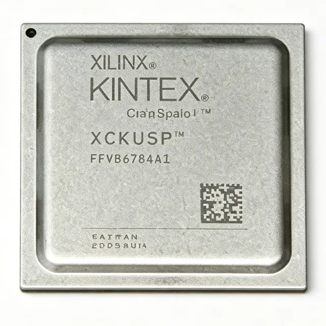
XCZU11EG-2FFVF1517I
XCZU11EG-2FFVF1517I - Zynq UltraScale+ MPSoC EG | AMD
The AMD XCZU11EG-2FFVF1517I is a Zynq® UltraScale+™ MPSoC EG device integrating a Quad ARM® Cortex®-A53 MPCore™ processor system with a Dual ARM® Cortex®-R5 real-time processor, an ARM Mali™-400 MP2 graphics processing unit, and a large programmable FPGA fabric in a 1517-ball FCBGA (40x40 mm) package. The -2 speed grade and industrial temperature grade (I) make it suitable for high-performance embedded applications requiring both hardware flexibility and software agility.
A System-on-Chip FPGA (SoC FPGA) combines a hard processor subsystem (PS) with programmable logic (PL) on a single die. This architecture enables designers to implement custom hardware accelerators, high-speed I/O interfaces, and real-time control functions in the PL while running an operating system such as Linux or VxWorks on the ARM cores in the PS. The Zynq UltraScale+ family sits at the high end of this hierarchy, offering advanced DSP engines, high-bandwidth DDR memory interfaces, and multi-gigabit transceivers that go beyond conventional FPGA or microcontroller solutions.
Key features of XCZU11EG-2FFVF1517I include 653,100 programmable logic cells, 597,120 FPGA registers, and 22,124,954 bits of block RAM. The PS supports a 1.3 GHz maximum ARM Cortex-A53 clock, a 600 MHz Cortex-R5 clock, and a 533 MHz Mali-400 MP2 clock. Connectivity interfaces include CANbus, EBI/EMI, Ethernet, I²C, MMC/SD/SDIO, SPI, UART/USART, and USB OTG, allowing direct interface to a wide range of peripheral devices and system networks.
The MPSoC is built on TSMC 16nm FinFET technology, enabling high logic density with manageable power dissipation. The -2 speed grade provides balanced timing performance for the programmable fabric, while the industrial temperature grade supports operation in demanding -40°C to +100°C environments. The 1517-ball FCBGA package with 40x40 mm body and 0.8 mm ball pitch enables high-density PCB routing for complex multi-rail power and high-speed serial links.
Typical applications include edge AI inference at industrial sites, 5G/4G baseband processing, radar and electronic warfare systems, broadcast and professional AV equipment, medical imaging, and data center SmartNICs. Designers should note that the device requires multiple power rails (VCCINT, VCCAUX, VCCBRAM, VCCO, PS rails) and careful sequencing; the recommended power-up sequence can be found in PG201 (Zynq UltraScale+ PCB Design). Adequate decoupling capacitors and a solid power delivery network are critical to achieving reliable high-speed operation.
When designing with this MPSoC, ensure that the boot mode pins are correctly configured for the desired QSPI, SD, or JTAG boot source. The PS can offload complex control tasks, while the PL implements latency-sensitive data path acceleration. Thermal management must consider both the PS and PL power consumption, and a heatsink or airflow is recommended for sustained high utilization.
見積もり
在庫あり