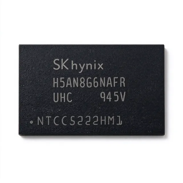
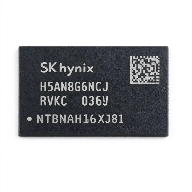
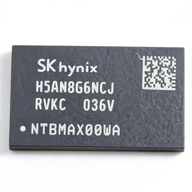
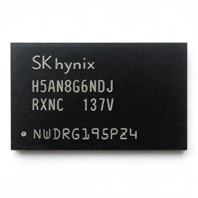
H5AN8G8NDJR-XNC
H5AN8G8NDJR-XNC - 8Gb DDR4-3200 SDRAM | SK Hynix
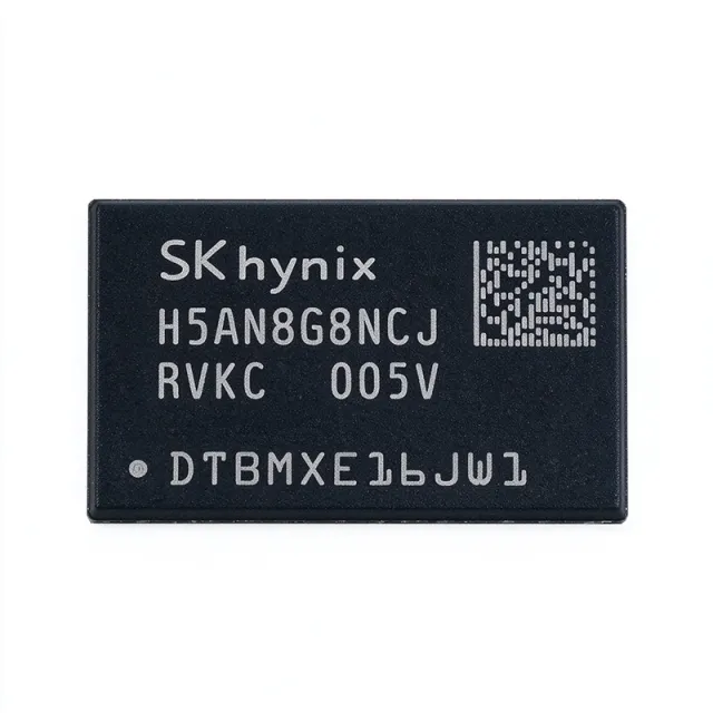
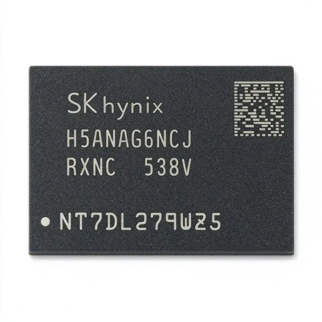
The SK Hynix H5AN8G8NDJR-XNC is an 8Gb DDR4 SDRAM memory IC organized as 1G x 8, designed for high-speed, low-voltage memory applications. It operates at a data rate of 3200MT/s (DDR4-3200, PC4-25600) with a supply voltage of 1.2V (VDD) and I/O voltage of 1.2V (VDDQ). The device is housed in a 78-ball FBGA package (7.5x11mm) and is RoHS compliant. It supports an operating temperature range of 0°C to +95°C (TC), making it suitable for a wide range of computing and embedded systems.
DDR4 SDRAM (Double Data Rate 4 Synchronous Dynamic Random-Access Memory) is a type of volatile memory that transfers data on both rising and falling edges of the clock signal, effectively doubling the data rate. It is the successor to DDR3 and offers higher speed, lower power consumption, and increased density. DDR4 operates at a lower voltage (1.2V) compared to DDR3 (1.5V), reducing power consumption by up to 40%. It is a critical component in modern computing systems, serving as the main memory for CPUs, GPUs, and SoCs, and is part of the memory hierarchy that includes cache, main memory, and storage.
Key features of the H5AN8G8NDJR-XNC include a bank group-based internal architecture that enhances performance, support for standard DDR4 features such as auto self-refresh, auto precharge, asynchronous reset, data mask, dynamic on-chip termination (DTC), ZQ calibration, write leveling, and CRC (Cyclic Redundancy Check) for data integrity. The device also supports on-die ECC (Error Correction Code) in some configurations, though this specific part is a standard non-ECC variant. The 78-ball FBGA package is optimized for high-density PCB layouts, and the device is available in tray packaging.
Technically, the H5AN8G8NDJR-XNC implements a 16n prefetch architecture, which is standard for DDR4, allowing it to achieve high bandwidth with a relatively low clock frequency. The device supports a burst length of 8 (BL8) and can be configured for burst chop (BC4). It also supports various power-saving modes, including active power-down, precharge power-down, and self-refresh, which are essential for mobile and embedded applications where power efficiency is critical. The device is designed to operate with a 1.2V supply, and it integrates a temperature sensor for thermal management.
Typical applications for the H5AN8G8NDJR-XNC include personal computers, servers, networking equipment, and embedded systems. Its high density and speed make it ideal for main memory in laptops and desktops, while its low power consumption is beneficial for battery-powered devices. In networking, it is used in routers and switches for packet buffering and routing tables. In embedded systems, it is used in industrial controllers, medical devices, and automotive infotainment systems. The device's wide temperature range and reliability make it suitable for industrial applications.
When designing with this component, ensure proper decoupling capacitors are placed close to the VDD and VDDQ pins to minimize power supply noise. The device requires a stable 1.2V supply and a reference voltage (VREF) for the I/O. Follow the PCB layout guidelines in the datasheet to maintain signal integrity at 3200MT/s, including controlled impedance traces and proper termination. Also, consider the thermal environment, as the device is rated for up to 95°C case temperature.
見積もり
お問い合わせ